US11397348B2 - Array substrate having convex component, method for fabricating the same, liquid crystal display panel, and display device - Google Patents
Array substrate having convex component, method for fabricating the same, liquid crystal display panel, and display device Download PDFInfo
- Publication number
- US11397348B2 US11397348B2 US16/300,255 US201816300255A US11397348B2 US 11397348 B2 US11397348 B2 US 11397348B2 US 201816300255 A US201816300255 A US 201816300255A US 11397348 B2 US11397348 B2 US 11397348B2
- Authority
- US
- United States
- Prior art keywords
- layer
- convex component
- thin film
- base substrate
- array substrate
- Prior art date
- Legal status (The legal status is an assumption and is not a legal conclusion. Google has not performed a legal analysis and makes no representation as to the accuracy of the status listed.)
- Active, expires
Links
Images


Classifications
-
- G—PHYSICS
- G02—OPTICS
- G02F—OPTICAL DEVICES OR ARRANGEMENTS FOR THE CONTROL OF LIGHT BY MODIFICATION OF THE OPTICAL PROPERTIES OF THE MEDIA OF THE ELEMENTS INVOLVED THEREIN; NON-LINEAR OPTICS; FREQUENCY-CHANGING OF LIGHT; OPTICAL LOGIC ELEMENTS; OPTICAL ANALOGUE/DIGITAL CONVERTERS
- G02F1/00—Devices or arrangements for the control of the intensity, colour, phase, polarisation or direction of light arriving from an independent light source, e.g. switching, gating or modulating; Non-linear optics
- G02F1/01—Devices or arrangements for the control of the intensity, colour, phase, polarisation or direction of light arriving from an independent light source, e.g. switching, gating or modulating; Non-linear optics for the control of the intensity, phase, polarisation or colour
- G02F1/13—Devices or arrangements for the control of the intensity, colour, phase, polarisation or direction of light arriving from an independent light source, e.g. switching, gating or modulating; Non-linear optics for the control of the intensity, phase, polarisation or colour based on liquid crystals, e.g. single liquid crystal display cells
- G02F1/133—Constructional arrangements; Operation of liquid crystal cells; Circuit arrangements
- G02F1/1333—Constructional arrangements; Manufacturing methods
- G02F1/1343—Electrodes
- G02F1/134309—Electrodes characterised by their geometrical arrangement
-
- G—PHYSICS
- G02—OPTICS
- G02F—OPTICAL DEVICES OR ARRANGEMENTS FOR THE CONTROL OF LIGHT BY MODIFICATION OF THE OPTICAL PROPERTIES OF THE MEDIA OF THE ELEMENTS INVOLVED THEREIN; NON-LINEAR OPTICS; FREQUENCY-CHANGING OF LIGHT; OPTICAL LOGIC ELEMENTS; OPTICAL ANALOGUE/DIGITAL CONVERTERS
- G02F1/00—Devices or arrangements for the control of the intensity, colour, phase, polarisation or direction of light arriving from an independent light source, e.g. switching, gating or modulating; Non-linear optics
- G02F1/01—Devices or arrangements for the control of the intensity, colour, phase, polarisation or direction of light arriving from an independent light source, e.g. switching, gating or modulating; Non-linear optics for the control of the intensity, phase, polarisation or colour
- G02F1/13—Devices or arrangements for the control of the intensity, colour, phase, polarisation or direction of light arriving from an independent light source, e.g. switching, gating or modulating; Non-linear optics for the control of the intensity, phase, polarisation or colour based on liquid crystals, e.g. single liquid crystal display cells
- G02F1/133—Constructional arrangements; Operation of liquid crystal cells; Circuit arrangements
- G02F1/1333—Constructional arrangements; Manufacturing methods
- G02F1/133345—Insulating layers
-
- G—PHYSICS
- G02—OPTICS
- G02F—OPTICAL DEVICES OR ARRANGEMENTS FOR THE CONTROL OF LIGHT BY MODIFICATION OF THE OPTICAL PROPERTIES OF THE MEDIA OF THE ELEMENTS INVOLVED THEREIN; NON-LINEAR OPTICS; FREQUENCY-CHANGING OF LIGHT; OPTICAL LOGIC ELEMENTS; OPTICAL ANALOGUE/DIGITAL CONVERTERS
- G02F1/00—Devices or arrangements for the control of the intensity, colour, phase, polarisation or direction of light arriving from an independent light source, e.g. switching, gating or modulating; Non-linear optics
- G02F1/01—Devices or arrangements for the control of the intensity, colour, phase, polarisation or direction of light arriving from an independent light source, e.g. switching, gating or modulating; Non-linear optics for the control of the intensity, phase, polarisation or colour
- G02F1/13—Devices or arrangements for the control of the intensity, colour, phase, polarisation or direction of light arriving from an independent light source, e.g. switching, gating or modulating; Non-linear optics for the control of the intensity, phase, polarisation or colour based on liquid crystals, e.g. single liquid crystal display cells
- G02F1/133—Constructional arrangements; Operation of liquid crystal cells; Circuit arrangements
- G02F1/1333—Constructional arrangements; Manufacturing methods
- G02F1/1335—Structural association of cells with optical devices, e.g. polarisers or reflectors
- G02F1/133553—Reflecting elements
-
- G—PHYSICS
- G02—OPTICS
- G02F—OPTICAL DEVICES OR ARRANGEMENTS FOR THE CONTROL OF LIGHT BY MODIFICATION OF THE OPTICAL PROPERTIES OF THE MEDIA OF THE ELEMENTS INVOLVED THEREIN; NON-LINEAR OPTICS; FREQUENCY-CHANGING OF LIGHT; OPTICAL LOGIC ELEMENTS; OPTICAL ANALOGUE/DIGITAL CONVERTERS
- G02F1/00—Devices or arrangements for the control of the intensity, colour, phase, polarisation or direction of light arriving from an independent light source, e.g. switching, gating or modulating; Non-linear optics
- G02F1/01—Devices or arrangements for the control of the intensity, colour, phase, polarisation or direction of light arriving from an independent light source, e.g. switching, gating or modulating; Non-linear optics for the control of the intensity, phase, polarisation or colour
- G02F1/13—Devices or arrangements for the control of the intensity, colour, phase, polarisation or direction of light arriving from an independent light source, e.g. switching, gating or modulating; Non-linear optics for the control of the intensity, phase, polarisation or colour based on liquid crystals, e.g. single liquid crystal display cells
- G02F1/133—Constructional arrangements; Operation of liquid crystal cells; Circuit arrangements
- G02F1/136—Liquid crystal cells structurally associated with a semi-conducting layer or substrate, e.g. cells forming part of an integrated circuit
- G02F1/1362—Active matrix addressed cells
- G02F1/136209—Light shielding layers, e.g. black matrix, incorporated in the active matrix substrate, e.g. structurally associated with the switching element
-
- G—PHYSICS
- G02—OPTICS
- G02F—OPTICAL DEVICES OR ARRANGEMENTS FOR THE CONTROL OF LIGHT BY MODIFICATION OF THE OPTICAL PROPERTIES OF THE MEDIA OF THE ELEMENTS INVOLVED THEREIN; NON-LINEAR OPTICS; FREQUENCY-CHANGING OF LIGHT; OPTICAL LOGIC ELEMENTS; OPTICAL ANALOGUE/DIGITAL CONVERTERS
- G02F1/00—Devices or arrangements for the control of the intensity, colour, phase, polarisation or direction of light arriving from an independent light source, e.g. switching, gating or modulating; Non-linear optics
- G02F1/01—Devices or arrangements for the control of the intensity, colour, phase, polarisation or direction of light arriving from an independent light source, e.g. switching, gating or modulating; Non-linear optics for the control of the intensity, phase, polarisation or colour
- G02F1/13—Devices or arrangements for the control of the intensity, colour, phase, polarisation or direction of light arriving from an independent light source, e.g. switching, gating or modulating; Non-linear optics for the control of the intensity, phase, polarisation or colour based on liquid crystals, e.g. single liquid crystal display cells
- G02F1/133—Constructional arrangements; Operation of liquid crystal cells; Circuit arrangements
- G02F1/136—Liquid crystal cells structurally associated with a semi-conducting layer or substrate, e.g. cells forming part of an integrated circuit
- G02F1/1362—Active matrix addressed cells
- G02F1/1368—Active matrix addressed cells in which the switching element is a three-electrode device
-
- G—PHYSICS
- G02—OPTICS
- G02F—OPTICAL DEVICES OR ARRANGEMENTS FOR THE CONTROL OF LIGHT BY MODIFICATION OF THE OPTICAL PROPERTIES OF THE MEDIA OF THE ELEMENTS INVOLVED THEREIN; NON-LINEAR OPTICS; FREQUENCY-CHANGING OF LIGHT; OPTICAL LOGIC ELEMENTS; OPTICAL ANALOGUE/DIGITAL CONVERTERS
- G02F1/00—Devices or arrangements for the control of the intensity, colour, phase, polarisation or direction of light arriving from an independent light source, e.g. switching, gating or modulating; Non-linear optics
- G02F1/01—Devices or arrangements for the control of the intensity, colour, phase, polarisation or direction of light arriving from an independent light source, e.g. switching, gating or modulating; Non-linear optics for the control of the intensity, phase, polarisation or colour
- G02F1/13—Devices or arrangements for the control of the intensity, colour, phase, polarisation or direction of light arriving from an independent light source, e.g. switching, gating or modulating; Non-linear optics for the control of the intensity, phase, polarisation or colour based on liquid crystals, e.g. single liquid crystal display cells
- G02F1/133—Constructional arrangements; Operation of liquid crystal cells; Circuit arrangements
- G02F1/1333—Constructional arrangements; Manufacturing methods
- G02F1/133357—Planarisation layers
-
- G—PHYSICS
- G02—OPTICS
- G02F—OPTICAL DEVICES OR ARRANGEMENTS FOR THE CONTROL OF LIGHT BY MODIFICATION OF THE OPTICAL PROPERTIES OF THE MEDIA OF THE ELEMENTS INVOLVED THEREIN; NON-LINEAR OPTICS; FREQUENCY-CHANGING OF LIGHT; OPTICAL LOGIC ELEMENTS; OPTICAL ANALOGUE/DIGITAL CONVERTERS
- G02F1/00—Devices or arrangements for the control of the intensity, colour, phase, polarisation or direction of light arriving from an independent light source, e.g. switching, gating or modulating; Non-linear optics
- G02F1/01—Devices or arrangements for the control of the intensity, colour, phase, polarisation or direction of light arriving from an independent light source, e.g. switching, gating or modulating; Non-linear optics for the control of the intensity, phase, polarisation or colour
- G02F1/13—Devices or arrangements for the control of the intensity, colour, phase, polarisation or direction of light arriving from an independent light source, e.g. switching, gating or modulating; Non-linear optics for the control of the intensity, phase, polarisation or colour based on liquid crystals, e.g. single liquid crystal display cells
- G02F1/133—Constructional arrangements; Operation of liquid crystal cells; Circuit arrangements
- G02F1/1333—Constructional arrangements; Manufacturing methods
- G02F1/1335—Structural association of cells with optical devices, e.g. polarisers or reflectors
- G02F1/13356—Structural association of cells with optical devices, e.g. polarisers or reflectors characterised by the placement of the optical elements
-
- G—PHYSICS
- G02—OPTICS
- G02F—OPTICAL DEVICES OR ARRANGEMENTS FOR THE CONTROL OF LIGHT BY MODIFICATION OF THE OPTICAL PROPERTIES OF THE MEDIA OF THE ELEMENTS INVOLVED THEREIN; NON-LINEAR OPTICS; FREQUENCY-CHANGING OF LIGHT; OPTICAL LOGIC ELEMENTS; OPTICAL ANALOGUE/DIGITAL CONVERTERS
- G02F1/00—Devices or arrangements for the control of the intensity, colour, phase, polarisation or direction of light arriving from an independent light source, e.g. switching, gating or modulating; Non-linear optics
- G02F1/01—Devices or arrangements for the control of the intensity, colour, phase, polarisation or direction of light arriving from an independent light source, e.g. switching, gating or modulating; Non-linear optics for the control of the intensity, phase, polarisation or colour
- G02F1/13—Devices or arrangements for the control of the intensity, colour, phase, polarisation or direction of light arriving from an independent light source, e.g. switching, gating or modulating; Non-linear optics for the control of the intensity, phase, polarisation or colour based on liquid crystals, e.g. single liquid crystal display cells
- G02F1/133—Constructional arrangements; Operation of liquid crystal cells; Circuit arrangements
- G02F1/136—Liquid crystal cells structurally associated with a semi-conducting layer or substrate, e.g. cells forming part of an integrated circuit
- G02F1/1362—Active matrix addressed cells
- G02F1/136231—Active matrix addressed cells for reducing the number of lithographic steps
- G02F1/136236—Active matrix addressed cells for reducing the number of lithographic steps using a grey or half tone lithographic process
-
- G—PHYSICS
- G02—OPTICS
- G02F—OPTICAL DEVICES OR ARRANGEMENTS FOR THE CONTROL OF LIGHT BY MODIFICATION OF THE OPTICAL PROPERTIES OF THE MEDIA OF THE ELEMENTS INVOLVED THEREIN; NON-LINEAR OPTICS; FREQUENCY-CHANGING OF LIGHT; OPTICAL LOGIC ELEMENTS; OPTICAL ANALOGUE/DIGITAL CONVERTERS
- G02F2201/00—Constructional arrangements not provided for in groups G02F1/00 - G02F7/00
- G02F2201/12—Constructional arrangements not provided for in groups G02F1/00 - G02F7/00 electrode
- G02F2201/123—Constructional arrangements not provided for in groups G02F1/00 - G02F7/00 electrode pixel
-
- G—PHYSICS
- G02—OPTICS
- G02F—OPTICAL DEVICES OR ARRANGEMENTS FOR THE CONTROL OF LIGHT BY MODIFICATION OF THE OPTICAL PROPERTIES OF THE MEDIA OF THE ELEMENTS INVOLVED THEREIN; NON-LINEAR OPTICS; FREQUENCY-CHANGING OF LIGHT; OPTICAL LOGIC ELEMENTS; OPTICAL ANALOGUE/DIGITAL CONVERTERS
- G02F2203/00—Function characteristic
- G02F2203/02—Function characteristic reflective
Definitions
- This disclosure relates to the field of display technologies, and particularly to an array substrate, a method for fabricating the same, a liquid crystal display panel and a display device.
- a backlight source to be provided as a light source for a liquid crystal panel in the related art to display an image is a light source located behind a Liquid Crystal Display (LCD), and a light emitting effect thereof may pose a direct influence on a visual effect of a Liquid Crystal Module (LCM).
- LCD Liquid Crystal Display
- Embodiments of the disclosure provide an array substrate including: a base substrate; a convex component located on the base substrate; a reflection layer overlying the convex component; a thin film transistor located above a film layer at which the reflection layer is located; a pixel electrode located above a film layer at which the thin film transistor is located; and a planarization layer located between the pixel electrode and the reflection layer.
- the planarization layer includes a gate insulation layer of the thin film transistor.
- the planarization layer further includes a first insulation layer located between the thin film transistor and the reflection layer.
- a material of the gate insulation layer is the same as a material of the first insulation layer.
- the thin film transistor is a thin film transistor with a bottom gate.
- an orthographic projection of the reflection layer onto the base substrate overlaps with an orthographic projection of the pixel electrode onto the base substrate.
- an orthographic projection of the convex component onto the base substrate does not overlap with an orthographic projection of the thin film transistor onto the base substrate.
- the convex component includes a plurality of layers of sub-convex component.
- a material of the convex component is a resin or a silicon nitride.
- the array substrate further includes a base layer located between the convex component and the base substrate.
- the embodiments of the disclosure further provide a liquid crystal display panel including the array substrate above according to the embodiments of the disclosure.
- the embodiments of the disclosure further provide a display device including the liquid crystal display panel above according to the embodiments of the disclosure.
- the embodiments of the disclosure further provide a method for fabricating the array substrate above, the method including: forming the convex component on the base substrate; forming the reflection layer above the convex component; forming the thin film transistor above the film layer at which the reflection layer is located; forming the pixel electrode above the film layer at which the thin film transistor is located; and forming the planarization layer after the reflection layer is formed, and before the pixel electrode is formed.
- forming the planarization layer includes: forming a gate insulation layer of the thin film transistor.
- forming the planarization layer further includes: forming a first insulation layer above the film layer at which the reflection layer is located.
- forming the convex component on the base substrate includes: forming the convex component on the base substrate using a half-tone or gray tone mask.
- the reflection layer and the pixel electrode are formed using the same mask.
- FIG. 1 is a schematic structural diagram of an array substrate according to embodiments of the disclosure in a sectional view;
- FIG. 2 is another schematic structural diagram of an array substrate according to the embodiments of the disclosure in a sectional view;
- FIG. 3 is still another schematic structural diagram of an array substrate according to the embodiments of the disclosure in a sectional view;
- FIG. 4 is yet another schematic structural diagram of an array substrate according to the embodiments of the disclosure in a sectional view.
- FIG. 5 is a schematic structural diagram of a liquid crystal display panel according to the embodiments of the disclosure in a sectional view.
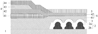
- an array substrate includes: a base substrate 1 ; a convex component 2 located on the base substrate 1 ; a reflection layer 3 overlying the convex component 2 ; a thin film transistor 4 located above a film layer at which the reflection layer 3 is located; a pixel electrode 5 located above a film layer at which the thin film transistor 4 is located; and a planarization layer 6 located between the pixel electrode 5 and the reflection layer 3 .
- the reflection layer 3 arranged between the pixel electrode 5 and the base substrate 1 can perform a function of reflecting light to thereby dispense with a backlight source so as to lower overall power consumption.
- the convex component 2 arranged between the reflection layer 3 and the base substrate 1 can make a surface of the reflection layer 3 overlying the convex component 2 concavo-convex to thereby satisfy a diffuse reflection condition of light so as to improve a lateral angle of view.
- the planarization layer 6 located on the reflection layer 3 with the concavo-convex surface can enable a surface of the pixel electrode 5 thereon to be planar, and the planar surface of the pixel electrode 5 can facilitate the maintenance of a morphology of an electric field formed between the pixel electrode 5 and a common electrode, as compared with the related art in which a diffuse reflection function is achieved directly using a pixel electrode with a concavo-convex surface.
- a material of the base substrate 1 will not be limited to any particular material, and for example, the base substrate is a glass substrate, or a substrate of another material, and a thickness thereof will not be limited to any particular thickness, but can be set as needed in reality.
- a material of the convex component 2 includes silicon nitride or a resin material, but there are a lower cost of the silicon nitride, and a higher adhesion strength of the silicon nitride to the base substrate 1 than the resin material, so the convex component 2 can be made of the silicon nitride to thereby save a cost, and dispense with a planarization operation before the convex component 2 is fabricated.
- a height of the convex component 2 will not be limited to any particular height, and for example, in order to enable the height of the convex component 2 to better satisfy the diffuse reflection condition of light, the height of the convex component 2 can be set in a range of 3000 to 4000 angstroms.
- an orthographic projection of the convex component 2 onto the base substrate 1 does not overlap with an orthographic projection of the thin film transistor 4 onto the base substrate 1 , that is, the convex component 2 is located in a valid display area of a pixel, and the thin film transistor 4 is located in a non-display area of the pixel.
- This design can avoid the concavo-convex convex component 2 from affecting the planarity and thus the performance of the thin film transistor 4 .
- the convex component 2 is located in the display area so that the reflection layer 3 overlying the convex component 2 has a concavo-convex surface in the display area to thereby satisfy the diffuse reflection condition of light so as to diffusely reflect light in the display area.
- the convex component 2 includes a plurality of layers of sub-convex component, and for example, as illustrated in FIG. 2 , each convex component includes a first layer of sub-convex component 2 a and a second layer of sub-convex component 2 b .
- the arrangement of the plurality of layers of sub-convex component can make the surface of the reflection layer 3 more concavo-convex to thereby better satisfy the diffuse reflection condition of light so that light rays can be better reflected diffusely to thereby further improve the lateral angle of view.
- the array substrate further includes a base layer 7 located between the convex component 2 and the base substrate 1 , where the base layer 7 can improve the adhesion strength between the convex component 2 and the base substrate 1 .
- a material of the base layer 7 can be the same as the material of the convex component 2 , and for example, both of them are silicon nitride.
- a thickness of the base layer will not be limited to any particular thickness, but can be set as needed in reality.
- the base layer 7 can cover the entire base substrate 1 so that the base layer 7 not only can further flatten the film layer at which the convex component 2 is arranged, but also can further improve the adhesion strength between the convex component 2 and the base substrate 1 to thereby avoid the convex component 2 from falling away.
- the thin film transistor 4 can be a thin film transistor with a top gate, or a thin film transistor with a bottom gate, although the embodiments of the disclosure will not be limited thereto.
- the thin film transistor 4 with the bottom gate includes a gate 41 , a gate insulation layer 42 , an active layer 43 , and a source-drain electrode 44 arranged in a stack manner in that order.
- the thin film transistor 4 with the top gate includes an active layer 43 , a gate insulation layer 42 , a gate 41 , an insulation layer 45 , and a source-drain electrode 44 arranged in a stack manner in that order.
- an orthographic projection of the reflection layer 3 onto the base substrate 1 can overlap with an orthographic projection of the pixel electrode 5 onto the base substrate 1 , so that the reflection layer 3 and the pixel electrode 5 can be fabricated using the same mask to thereby save a fabrication cost.
- the reflection layer 3 can extend to an area below the thin film transistor 4 , and act as a light-shielding layer, so that the reflection layer 3 shields the active layer 43 to thereby avoid leakage current from affecting the display driving.
- the orthographic projection of the convex component 2 onto the base substrate 1 does not overlap with the orthographic projection of the thin film transistor 4 onto the base substrate 1 , a surface of the reflection layer 3 below the thin film transistor 4 is so planar that the thin film transistor 4 located above will not be hindered from being fabricated.
- a material of the reflection layer 3 can be a metal material, for example, or can be another material, or a mixture of both, where the metal material can be copper, iron, aluminum, a compound of a plurality of metal materials, etc.
- the reflection layer 3 can be a single layer of metal material, or a plurality of layers of metal materials.
- the planarization layer 6 includes the gate insulation layer 42 of the thin film transistor 4 .
- the gate insulation layer 42 is arranged between the gate 41 and the active layer 43 , and the gate insulation layer 42 can function for planarization. Further, in order to optimize the planarization function, the gate insulation layer 42 can be improved in thickness as appropriate, but the gate insulation layer 42 shall not be too thick; otherwise the on-voltage of the gate 41 may be affected that power consumption for driving may become higher.
- the planarization layer 6 furthers include a first insulation layer 61 located between the thin film transistor 4 and the reflection layer 3 .
- the first insulation layer 61 located between the thin film transistor 4 and the reflection layer 3 not only can function for a better planarization, but also can insulate the reflection layer 3 from the thin film transistor 4 so that a pattern of the reflection layer 3 can be arranged over an entire surface without being limited to a pattern of the thin film transistor 4 . Further, the first insulation layer 61 can isolate signal interference between the reflection layer 3 and the thin film transistor 4 so that the pixel electrode 5 can be driven normally.
- a material of the first insulation layer 61 is silicon nitride or a resin, although the embodiments of the disclosure will not be limited thereto.
- a material of the gate insulation layer 42 is the same as the material of the first insulation layer 61 .
- the array substrate can further include other existing structural layers, and a repeated description thereof will be omitted here.
- the embodiments of the disclosure further provide a liquid crystal display panel as illustrated in FIG. 5 , which includes the array substrate 01 above according to the embodiments of the disclosure, and further includes an opposite substrate 02 , and a liquid crystal layer 03 located between the opposite substrate 02 and the array substrate 01 .
- a common electrode layer 8 cooperating with the pixel electrode 5 to generate an electric field for controlling the liquid crystal layer 03 can be arranged on a side of the opposite substrate 02 facing the array substrate 01 , or can be arranged on a side of the array substrate 01 facing the opposite substrate 02 , although the embodiments of the disclosure will not be limited thereto.
- the embodiments of the disclosure further provide a display device including the liquid crystal display panel above according to the embodiments of the disclosure.
- the display device can be a smart phone, a liquid crystal television, a tablet computer, a Light Emitting Diode (LED) display screen, LCD, or any product with a display function.
- LED Light Emitting Diode
- the embodiments of the disclosure further provide a method for fabricating the array substrate above, where the method includes the following operations.
- forming the planarization layer includes forming a gate insulation layer of the thin film transistor, that is, the gate insulation layer is taken as a part of the planarization layer.
- forming the planarization layer further includes: forming a first insulation layer above the film layer at which the reflection layer is located, that is, the first insulation layer between the reflection layer and the thin film transistor is taken as another part of the planarization layer, and the first insulation layer overlaps with the gate insulation layer to constitute the planarization layer with such a thickness that can make the layer planar without affecting the planarity of the fabricated pixel electrode.
- forming the convex component on the base substrate includes: forming the convex component on the base substrate using a half-tone or gray tone mask.
- the convex component in order to provide a satisfactory height, e.g., 4000 angstroms, of the convex component, can be made in a plurality of layers of sub-convex component; and referring to FIG. 2 , for example, each convex component 2 is fabricated in two components by firstly fabricating a first layer of sub-convex component 2 a on a base layer using a Half-Tone Mask (HTM), and then stacking a second layer of sub-convex component 2 b using the Half-Tone Mask (HTM) for fabricating the first layer of sub-convex component 2 a.
- HTM Half-Tone Mask
- the reflection layer and the pixel electrode can be formed using the same mask.
- the reflection layer and the pixel electrode can be fabricated using the same mask without any additional mask; and can be fabricated in another area than the thin film transistor without hindering a pixel from being driven.
- the method for fabricating the array substrate according to the embodiments of the disclosure includes following operations.
- the first operation is to fabricate a base layer 7 on a base substrate 1 as a base; or the base layer 7 may not be fabricated, but the base substrate 1 may be a base directly, that is, this operation can be omitted.
- the second operation is to form a convex component 2 in a display area above the base layer 7 in an etching process using a first mask, where a height of the convex component 2 can be set as needed in reality.
- the third operation is to fabricate a reflection layer 3 above the convex component 2 using a second mask.
- the fourth operation is to fabricate a first insulation layer 61 above the reflection layer 3 .
- the fifth operation is to fabricate a gate 41 , a gate insulation layer 42 , an active layer 43 , and a source-drain electrode 44 in that order in a non-display area above the first insulation layer 61 .
- the sixth operation is to form a pixel electrode 5 in the display area using the second mask.
Abstract
Description
Claims (17)
Applications Claiming Priority (3)
| Application Number | Priority Date | Filing Date | Title |
|---|---|---|---|
| CN201710369924.2A CN107065328A (en) | 2017-05-23 | 2017-05-23 | A kind of dot structure, display panel, display device and pixel structure preparation method |
| CN201710369924.2 | 2017-05-23 | ||
| PCT/CN2018/079887 WO2018214628A1 (en) | 2017-05-23 | 2018-03-21 | Array substrate and manufacturing method therefor, and liquid crystal display panel and display apparatus |
Publications (2)
| Publication Number | Publication Date |
|---|---|
| US20190155099A1 US20190155099A1 (en) | 2019-05-23 |
| US11397348B2 true US11397348B2 (en) | 2022-07-26 |
Family
ID=59610465
Family Applications (1)
| Application Number | Title | Priority Date | Filing Date |
|---|---|---|---|
| US16/300,255 Active 2039-08-11 US11397348B2 (en) | 2017-05-23 | 2018-03-21 | Array substrate having convex component, method for fabricating the same, liquid crystal display panel, and display device |
Country Status (3)
| Country | Link |
|---|---|
| US (1) | US11397348B2 (en) |
| CN (1) | CN107065328A (en) |
| WO (1) | WO2018214628A1 (en) |
Families Citing this family (3)
| Publication number | Priority date | Publication date | Assignee | Title |
|---|---|---|---|---|
| CN107065328A (en) | 2017-05-23 | 2017-08-18 | 京东方科技集团股份有限公司 | A kind of dot structure, display panel, display device and pixel structure preparation method |
| WO2022134029A1 (en) * | 2020-12-25 | 2022-06-30 | 京东方科技集团股份有限公司 | Display panel, method for manufacturing display panel, and display device |
| CN115718387B (en) * | 2022-11-28 | 2023-11-07 | 京东方科技集团股份有限公司 | Reflection type array substrate and manufacturing method thereof, display device and manufacturing method thereof |
Citations (33)
| Publication number | Priority date | Publication date | Assignee | Title |
|---|---|---|---|---|
| CN1118077A (en) | 1994-05-12 | 1996-03-06 | 卡西欧计算机公司 | Reflection type color liquid crystal display device |
| US5500750A (en) * | 1993-03-24 | 1996-03-19 | Sharp Kabushiki Kaisha | Manufacturing method of reflection type liquid crystal display devices having light shield elements and reflective electrodes formed of same material |
| US5940154A (en) * | 1996-11-05 | 1999-08-17 | Nec Corporation | Reflection type liquid crystal display and method of fabricating the same |
| CN1246634A (en) | 1998-07-31 | 2000-03-08 | 株式会社日立制作所 | Diffuse reflection plate and liquid display device using the plate and manufacturing method thereof |
| US6208395B1 (en) * | 1995-08-16 | 2001-03-27 | Nec Corporation | Reflective liquid crystal display and method for fabricating the same |
| US6341002B1 (en) * | 1998-10-15 | 2002-01-22 | Sharp Kabushiki Kaisha | Liquid crystal display device |
| US6407784B1 (en) * | 1998-03-11 | 2002-06-18 | Nec Corporation | Reflection type liquid crystal display and method of fabricating the same |
| US20020118326A1 (en) * | 2001-02-14 | 2002-08-29 | Michiaki Sakamoto | Active-matrix addressed reflective LCD and method of fabricating the same |
| US20020196396A1 (en) * | 2001-06-22 | 2002-12-26 | Nec Corporation | Reflection plate, manufacturing method thereof, liquid crystal display device, and manufacturing method thereof |
| US6532045B2 (en) * | 1999-12-28 | 2003-03-11 | Lg. Philips Lcd Co. Ltd. | Transflective liquid crystal display device and method of manufacturing the same |
| US6654176B2 (en) * | 2001-08-07 | 2003-11-25 | Hitachi, Ltd. | Microlens array, a method for making a transfer master pattern for microlens array, a concave and convex pattern obtained from the transfer master pattern, a laminate for transfer, a diffuse reflection plate and a liquid crystal display device |
| US20040070709A1 (en) * | 2000-01-14 | 2004-04-15 | Hiroshi Kanou | Liquid crystal display apparatus with protective insulating film for switching element and production method thereof |
| US20040119901A1 (en) * | 2002-12-20 | 2004-06-24 | Won-Seok Kang | Reflective liquid crystal display device and fabricating method thereof |
| JP2004184565A (en) | 2002-12-02 | 2004-07-02 | Casio Comput Co Ltd | Reflective display device |
| US20040135944A1 (en) | 2002-04-15 | 2004-07-15 | Lg.Philips Lcd Co., Ltd. | Reflection-type liquid crystal display device and method of fabricating the same |
| US6879359B1 (en) * | 1998-11-18 | 2005-04-12 | Nec Lcd Technologies, Ltd. | Reflection type liquid crystal display provided with reflective layer, coplanar gate electrode, color filter layer and transparent pixel electrode and manufacture method thereof |
| US6881535B2 (en) * | 2001-07-03 | 2005-04-19 | Nec Lcd Technologies, Ltd. | Method for producing liquid crystal display apparatus |
| US20050083454A1 (en) * | 2001-10-04 | 2005-04-21 | Naoki Sumi | Optical reflector and display device using it |
| US20050083461A1 (en) * | 2003-10-16 | 2005-04-21 | Lg.Philips Lcd Co., Ltd. | Transflective-type liquid crystal display device and method of fabricating the same |
| US20050094070A1 (en) * | 2003-11-04 | 2005-05-05 | Innolux Display Corp. | Liquid crystal display with a planarization layer having black resin |
| US6900084B1 (en) * | 2000-05-09 | 2005-05-31 | Semiconductor Energy Laboratory Co., Ltd. | Semiconductor device having a display device |
| US20070263288A1 (en) * | 2004-12-10 | 2007-11-15 | Yusuke Tsubota | Diffusive Reflecting Structure and Its Manufacturing Method, and Display Device Using It |
| KR20080004989A (en) | 2006-07-07 | 2008-01-10 | 삼성전자주식회사 | Method for fabricating thin film transistor array substrate |
| US7440050B2 (en) * | 2003-09-15 | 2008-10-21 | Tpo Hong Kong Holding Limited | Reflective structure having a directivity of diffuse reflection and apparatus with it |
| US7760321B2 (en) * | 2006-02-20 | 2010-07-20 | Samsung Electronics Co., Ltd. | Method of manufacturing a liquid crystal display device |
| US8035781B2 (en) * | 2002-03-01 | 2011-10-11 | Semiconductor Energy Laboratory Co., Ltd. | Liquid crystal display device |
| US20160035807A1 (en) * | 2013-09-27 | 2016-02-04 | Boe Technology Group Co., Ltd. | Oled pixel structure and oled display device |
| US20160041414A1 (en) * | 2014-01-09 | 2016-02-11 | Boe Technology Group Co., Ltd. | Array substrate, liquid crystal display panel and display device |
| US20160349558A1 (en) * | 2015-05-27 | 2016-12-01 | Semiconductor Energy Laboratory Co., Ltd. | Touch panel |
| US20160358948A1 (en) * | 2014-12-23 | 2016-12-08 | Boe Technology Group Co. Ltd. | Display Substrate, Manufacturing Method Thereof, and Display Device |
| US20160365069A1 (en) * | 2015-06-10 | 2016-12-15 | Boe Technology Group Co., Ltd. | Array substrate, manufacturing method thereof, control method, control assembly, and display device |
| US20170053608A1 (en) * | 2015-04-21 | 2017-02-23 | Boe Technology Group Co., Ltd | Array substrate, display panel and display apparatus containing the same, and method for driving the same |
| CN107065328A (en) | 2017-05-23 | 2017-08-18 | 京东方科技集团股份有限公司 | A kind of dot structure, display panel, display device and pixel structure preparation method |
-
2017
- 2017-05-23 CN CN201710369924.2A patent/CN107065328A/en active Pending
-
2018
- 2018-03-21 US US16/300,255 patent/US11397348B2/en active Active
- 2018-03-21 WO PCT/CN2018/079887 patent/WO2018214628A1/en active Application Filing
Patent Citations (37)
| Publication number | Priority date | Publication date | Assignee | Title |
|---|---|---|---|---|
| US5500750A (en) * | 1993-03-24 | 1996-03-19 | Sharp Kabushiki Kaisha | Manufacturing method of reflection type liquid crystal display devices having light shield elements and reflective electrodes formed of same material |
| US5734455A (en) | 1994-05-12 | 1998-03-31 | Casio Computer Co., Ltd. | Reflective birefringent type color liquid crystal display employing black mask |
| CN1118077A (en) | 1994-05-12 | 1996-03-06 | 卡西欧计算机公司 | Reflection type color liquid crystal display device |
| US6208395B1 (en) * | 1995-08-16 | 2001-03-27 | Nec Corporation | Reflective liquid crystal display and method for fabricating the same |
| US5940154A (en) * | 1996-11-05 | 1999-08-17 | Nec Corporation | Reflection type liquid crystal display and method of fabricating the same |
| US6407784B1 (en) * | 1998-03-11 | 2002-06-18 | Nec Corporation | Reflection type liquid crystal display and method of fabricating the same |
| CN1246634A (en) | 1998-07-31 | 2000-03-08 | 株式会社日立制作所 | Diffuse reflection plate and liquid display device using the plate and manufacturing method thereof |
| US20020054259A1 (en) * | 1998-07-31 | 2002-05-09 | Katsuyuki Funahata | Diffused reflector, liquid crystal display device constructed to use the reflector, and manufacture of the same |
| US6341002B1 (en) * | 1998-10-15 | 2002-01-22 | Sharp Kabushiki Kaisha | Liquid crystal display device |
| US6879359B1 (en) * | 1998-11-18 | 2005-04-12 | Nec Lcd Technologies, Ltd. | Reflection type liquid crystal display provided with reflective layer, coplanar gate electrode, color filter layer and transparent pixel electrode and manufacture method thereof |
| US6532045B2 (en) * | 1999-12-28 | 2003-03-11 | Lg. Philips Lcd Co. Ltd. | Transflective liquid crystal display device and method of manufacturing the same |
| US7705945B2 (en) * | 2000-01-14 | 2010-04-27 | Nec Corporation | Method of producing a reflective liquid crystal display |
| US20040070709A1 (en) * | 2000-01-14 | 2004-04-15 | Hiroshi Kanou | Liquid crystal display apparatus with protective insulating film for switching element and production method thereof |
| US6900084B1 (en) * | 2000-05-09 | 2005-05-31 | Semiconductor Energy Laboratory Co., Ltd. | Semiconductor device having a display device |
| US20020118326A1 (en) * | 2001-02-14 | 2002-08-29 | Michiaki Sakamoto | Active-matrix addressed reflective LCD and method of fabricating the same |
| US20020196396A1 (en) * | 2001-06-22 | 2002-12-26 | Nec Corporation | Reflection plate, manufacturing method thereof, liquid crystal display device, and manufacturing method thereof |
| US6881535B2 (en) * | 2001-07-03 | 2005-04-19 | Nec Lcd Technologies, Ltd. | Method for producing liquid crystal display apparatus |
| US6654176B2 (en) * | 2001-08-07 | 2003-11-25 | Hitachi, Ltd. | Microlens array, a method for making a transfer master pattern for microlens array, a concave and convex pattern obtained from the transfer master pattern, a laminate for transfer, a diffuse reflection plate and a liquid crystal display device |
| US20050083454A1 (en) * | 2001-10-04 | 2005-04-21 | Naoki Sumi | Optical reflector and display device using it |
| US8035781B2 (en) * | 2002-03-01 | 2011-10-11 | Semiconductor Energy Laboratory Co., Ltd. | Liquid crystal display device |
| US20040135944A1 (en) | 2002-04-15 | 2004-07-15 | Lg.Philips Lcd Co., Ltd. | Reflection-type liquid crystal display device and method of fabricating the same |
| JP2004184565A (en) | 2002-12-02 | 2004-07-02 | Casio Comput Co Ltd | Reflective display device |
| US20040119901A1 (en) * | 2002-12-20 | 2004-06-24 | Won-Seok Kang | Reflective liquid crystal display device and fabricating method thereof |
| US7440050B2 (en) * | 2003-09-15 | 2008-10-21 | Tpo Hong Kong Holding Limited | Reflective structure having a directivity of diffuse reflection and apparatus with it |
| US20050083461A1 (en) * | 2003-10-16 | 2005-04-21 | Lg.Philips Lcd Co., Ltd. | Transflective-type liquid crystal display device and method of fabricating the same |
| US20050094070A1 (en) * | 2003-11-04 | 2005-05-05 | Innolux Display Corp. | Liquid crystal display with a planarization layer having black resin |
| CN101103302A (en) | 2004-12-10 | 2008-01-09 | 统宝香港控股有限公司 | Diffusive reflecting structure and its manufacturing method, and display device using it |
| US20070263288A1 (en) * | 2004-12-10 | 2007-11-15 | Yusuke Tsubota | Diffusive Reflecting Structure and Its Manufacturing Method, and Display Device Using It |
| US7760321B2 (en) * | 2006-02-20 | 2010-07-20 | Samsung Electronics Co., Ltd. | Method of manufacturing a liquid crystal display device |
| KR20080004989A (en) | 2006-07-07 | 2008-01-10 | 삼성전자주식회사 | Method for fabricating thin film transistor array substrate |
| US20160035807A1 (en) * | 2013-09-27 | 2016-02-04 | Boe Technology Group Co., Ltd. | Oled pixel structure and oled display device |
| US20160041414A1 (en) * | 2014-01-09 | 2016-02-11 | Boe Technology Group Co., Ltd. | Array substrate, liquid crystal display panel and display device |
| US20160358948A1 (en) * | 2014-12-23 | 2016-12-08 | Boe Technology Group Co. Ltd. | Display Substrate, Manufacturing Method Thereof, and Display Device |
| US20170053608A1 (en) * | 2015-04-21 | 2017-02-23 | Boe Technology Group Co., Ltd | Array substrate, display panel and display apparatus containing the same, and method for driving the same |
| US20160349558A1 (en) * | 2015-05-27 | 2016-12-01 | Semiconductor Energy Laboratory Co., Ltd. | Touch panel |
| US20160365069A1 (en) * | 2015-06-10 | 2016-12-15 | Boe Technology Group Co., Ltd. | Array substrate, manufacturing method thereof, control method, control assembly, and display device |
| CN107065328A (en) | 2017-05-23 | 2017-08-18 | 京东方科技集团股份有限公司 | A kind of dot structure, display panel, display device and pixel structure preparation method |
Non-Patent Citations (2)
| Title |
|---|
| International Search Report for PCT/CN2018/079887 dated Jun. 25, 2018. |
| Office Action for corresponding Chinese Application 201710369924.2 dated Feb. 22, 2019. |
Also Published As
| Publication number | Publication date |
|---|---|
| US20190155099A1 (en) | 2019-05-23 |
| WO2018214628A1 (en) | 2018-11-29 |
| CN107065328A (en) | 2017-08-18 |
Similar Documents
| Publication | Publication Date | Title |
|---|---|---|
| US10847585B2 (en) | Organic light emitting display device including a sound generating apparatus | |
| US20200328264A1 (en) | Oled substrate, manufacturing method thereof and display device | |
| US20210336166A1 (en) | Flexible display panel | |
| EP3156841A1 (en) | Display base plate, display panel and display device | |
| US20140036179A1 (en) | Liquid crystal display panel and display device | |
| US20180173049A1 (en) | Metal wire grid polarizer and liquid crystal display device | |
| US11397348B2 (en) | Array substrate having convex component, method for fabricating the same, liquid crystal display panel, and display device | |
| US11049886B2 (en) | Thin-film transistor array substrate and manufacturing method thereof | |
| US7907235B2 (en) | Dual liquid crystal display (LCD) | |
| US20170133402A1 (en) | An array substrate and a display device | |
| CN112038379B (en) | Pixel array substrate | |
| US9502439B2 (en) | Array substrate and a display device | |
| WO2013044783A1 (en) | Array substrate and method for manufacturing same and display device | |
| US9335587B2 (en) | Liquid crystal cell and method for manufacturing the same | |
| WO2018228109A1 (en) | Coa substrate, manufacturing method therefor, display panel, and display device | |
| WO2016165291A1 (en) | Array substrate, display panel and display device | |
| CN111290182A (en) | Liquid crystal display panel | |
| JP2013003220A (en) | Liquid crystal display device and mother substrate | |
| WO2020155452A1 (en) | Special-shaped display device | |
| US20150168784A1 (en) | Liquid crystal display device | |
| WO2021238343A1 (en) | Display panel and display device | |
| US20190227379A1 (en) | Array substrate and method for manufacturing the same, display panel and method for manufacturing the same | |
| JP3194456U (en) | Display panel and display device | |
| CN116169148A (en) | Array substrate, manufacturing method thereof and display device | |
| CN100373221C (en) | Display panels and electronic |
Legal Events
| Date | Code | Title | Description |
|---|---|---|---|
| AS | Assignment |
Owner name: BEIJING BOE OPTOELECTRONICS TECHNOLOGY CO., LTD., CHINA Free format text: ASSIGNMENT OF ASSIGNORS INTEREST;ASSIGNORS:FANG, HAOBO;XUE, YANNA;BAO, ZHIYING;AND OTHERS;REEL/FRAME:047462/0453 Effective date: 20180823 Owner name: BOE TECHNOLOGY GROUP CO., LTD., CHINA Free format text: ASSIGNMENT OF ASSIGNORS INTEREST;ASSIGNORS:FANG, HAOBO;XUE, YANNA;BAO, ZHIYING;AND OTHERS;REEL/FRAME:047462/0453 Effective date: 20180823 Owner name: BEIJING BOE OPTOELECTRONICS TECHNOLOGY CO., LTD., Free format text: ASSIGNMENT OF ASSIGNORS INTEREST;ASSIGNORS:FANG, HAOBO;XUE, YANNA;BAO, ZHIYING;AND OTHERS;REEL/FRAME:047462/0453 Effective date: 20180823 |
|
| FEPP | Fee payment procedure |
Free format text: ENTITY STATUS SET TO UNDISCOUNTED (ORIGINAL EVENT CODE: BIG.); ENTITY STATUS OF PATENT OWNER: LARGE ENTITY |
|
| STPP | Information on status: patent application and granting procedure in general |
Free format text: DOCKETED NEW CASE - READY FOR EXAMINATION |
|
| STPP | Information on status: patent application and granting procedure in general |
Free format text: NON FINAL ACTION MAILED |
|
| STPP | Information on status: patent application and granting procedure in general |
Free format text: NON FINAL ACTION MAILED |
|
| STPP | Information on status: patent application and granting procedure in general |
Free format text: RESPONSE TO NON-FINAL OFFICE ACTION ENTERED AND FORWARDED TO EXAMINER |
|
| STPP | Information on status: patent application and granting procedure in general |
Free format text: FINAL REJECTION MAILED |
|
| STPP | Information on status: patent application and granting procedure in general |
Free format text: RESPONSE AFTER FINAL ACTION FORWARDED TO EXAMINER |
|
| STPP | Information on status: patent application and granting procedure in general |
Free format text: NOTICE OF ALLOWANCE MAILED -- APPLICATION RECEIVED IN OFFICE OF PUBLICATIONS |
|
| STPP | Information on status: patent application and granting procedure in general |
Free format text: PUBLICATIONS -- ISSUE FEE PAYMENT VERIFIED |
|
| STCF | Information on status: patent grant |
Free format text: PATENTED CASE |