US11393855B2 - Photoelectric conversion apparatus, photoelectric conversion system, and moving object - Google Patents
Photoelectric conversion apparatus, photoelectric conversion system, and moving object Download PDFInfo
- Publication number
- US11393855B2 US11393855B2 US16/693,114 US201916693114A US11393855B2 US 11393855 B2 US11393855 B2 US 11393855B2 US 201916693114 A US201916693114 A US 201916693114A US 11393855 B2 US11393855 B2 US 11393855B2
- Authority
- US
- United States
- Prior art keywords
- semiconductor region
- photoelectric conversion
- conversion apparatus
- depth
- conductivity type
- Prior art date
- Legal status (The legal status is an assumption and is not a legal conclusion. Google has not performed a legal analysis and makes no representation as to the accuracy of the status listed.)
- Active, expires
Links
Images


Classifications
-
- H01L27/14603—
-
- G—PHYSICS
- G06—COMPUTING OR CALCULATING; COUNTING
- G06T—IMAGE DATA PROCESSING OR GENERATION, IN GENERAL
- G06T7/00—Image analysis
- G06T7/50—Depth or shape recovery
- G06T7/55—Depth or shape recovery from multiple images
- G06T7/593—Depth or shape recovery from multiple images from stereo images
-
- H01L27/1462—
-
- H01L27/14627—
-
- H01L27/14629—
-
- H01L27/1464—
-
- H01L27/14643—
-
- H01L31/02161—
-
- H01L31/022466—
-
- H01L31/035272—
-
- H—ELECTRICITY
- H04—ELECTRIC COMMUNICATION TECHNIQUE
- H04N—PICTORIAL COMMUNICATION, e.g. TELEVISION
- H04N23/00—Cameras or camera modules comprising electronic image sensors; Control thereof
- H04N23/50—Constructional details
- H04N23/54—Mounting of pick-up tubes, electronic image sensors, deviation or focusing coils
-
- H04N5/2253—
-
- H—ELECTRICITY
- H10—SEMICONDUCTOR DEVICES; ELECTRIC SOLID-STATE DEVICES NOT OTHERWISE PROVIDED FOR
- H10F—INORGANIC SEMICONDUCTOR DEVICES SENSITIVE TO INFRARED RADIATION, LIGHT, ELECTROMAGNETIC RADIATION OF SHORTER WAVELENGTH OR CORPUSCULAR RADIATION
- H10F39/00—Integrated devices, or assemblies of multiple devices, comprising at least one element covered by group H10F30/00, e.g. radiation detectors comprising photodiode arrays
- H10F39/10—Integrated devices
- H10F39/12—Image sensors
- H10F39/18—Complementary metal-oxide-semiconductor [CMOS] image sensors; Photodiode array image sensors
-
- H—ELECTRICITY
- H10—SEMICONDUCTOR DEVICES; ELECTRIC SOLID-STATE DEVICES NOT OTHERWISE PROVIDED FOR
- H10F—INORGANIC SEMICONDUCTOR DEVICES SENSITIVE TO INFRARED RADIATION, LIGHT, ELECTROMAGNETIC RADIATION OF SHORTER WAVELENGTH OR CORPUSCULAR RADIATION
- H10F39/00—Integrated devices, or assemblies of multiple devices, comprising at least one element covered by group H10F30/00, e.g. radiation detectors comprising photodiode arrays
- H10F39/10—Integrated devices
- H10F39/12—Image sensors
- H10F39/199—Back-illuminated image sensors
-
- H—ELECTRICITY
- H10—SEMICONDUCTOR DEVICES; ELECTRIC SOLID-STATE DEVICES NOT OTHERWISE PROVIDED FOR
- H10F—INORGANIC SEMICONDUCTOR DEVICES SENSITIVE TO INFRARED RADIATION, LIGHT, ELECTROMAGNETIC RADIATION OF SHORTER WAVELENGTH OR CORPUSCULAR RADIATION
- H10F39/00—Integrated devices, or assemblies of multiple devices, comprising at least one element covered by group H10F30/00, e.g. radiation detectors comprising photodiode arrays
- H10F39/80—Constructional details of image sensors
- H10F39/802—Geometry or disposition of elements in pixels, e.g. address-lines or gate electrodes
-
- H—ELECTRICITY
- H10—SEMICONDUCTOR DEVICES; ELECTRIC SOLID-STATE DEVICES NOT OTHERWISE PROVIDED FOR
- H10F—INORGANIC SEMICONDUCTOR DEVICES SENSITIVE TO INFRARED RADIATION, LIGHT, ELECTROMAGNETIC RADIATION OF SHORTER WAVELENGTH OR CORPUSCULAR RADIATION
- H10F39/00—Integrated devices, or assemblies of multiple devices, comprising at least one element covered by group H10F30/00, e.g. radiation detectors comprising photodiode arrays
- H10F39/80—Constructional details of image sensors
- H10F39/803—Pixels having integrated switching, control, storage or amplification elements
- H10F39/8033—Photosensitive area
-
- H—ELECTRICITY
- H10—SEMICONDUCTOR DEVICES; ELECTRIC SOLID-STATE DEVICES NOT OTHERWISE PROVIDED FOR
- H10F—INORGANIC SEMICONDUCTOR DEVICES SENSITIVE TO INFRARED RADIATION, LIGHT, ELECTROMAGNETIC RADIATION OF SHORTER WAVELENGTH OR CORPUSCULAR RADIATION
- H10F39/00—Integrated devices, or assemblies of multiple devices, comprising at least one element covered by group H10F30/00, e.g. radiation detectors comprising photodiode arrays
- H10F39/80—Constructional details of image sensors
- H10F39/805—Coatings
-
- H—ELECTRICITY
- H10—SEMICONDUCTOR DEVICES; ELECTRIC SOLID-STATE DEVICES NOT OTHERWISE PROVIDED FOR
- H10F—INORGANIC SEMICONDUCTOR DEVICES SENSITIVE TO INFRARED RADIATION, LIGHT, ELECTROMAGNETIC RADIATION OF SHORTER WAVELENGTH OR CORPUSCULAR RADIATION
- H10F39/00—Integrated devices, or assemblies of multiple devices, comprising at least one element covered by group H10F30/00, e.g. radiation detectors comprising photodiode arrays
- H10F39/80—Constructional details of image sensors
- H10F39/806—Optical elements or arrangements associated with the image sensors
- H10F39/8063—Microlenses
-
- H—ELECTRICITY
- H10—SEMICONDUCTOR DEVICES; ELECTRIC SOLID-STATE DEVICES NOT OTHERWISE PROVIDED FOR
- H10F—INORGANIC SEMICONDUCTOR DEVICES SENSITIVE TO INFRARED RADIATION, LIGHT, ELECTROMAGNETIC RADIATION OF SHORTER WAVELENGTH OR CORPUSCULAR RADIATION
- H10F39/00—Integrated devices, or assemblies of multiple devices, comprising at least one element covered by group H10F30/00, e.g. radiation detectors comprising photodiode arrays
- H10F39/80—Constructional details of image sensors
- H10F39/806—Optical elements or arrangements associated with the image sensors
- H10F39/8067—Reflectors
-
- H—ELECTRICITY
- H10—SEMICONDUCTOR DEVICES; ELECTRIC SOLID-STATE DEVICES NOT OTHERWISE PROVIDED FOR
- H10F—INORGANIC SEMICONDUCTOR DEVICES SENSITIVE TO INFRARED RADIATION, LIGHT, ELECTROMAGNETIC RADIATION OF SHORTER WAVELENGTH OR CORPUSCULAR RADIATION
- H10F77/00—Constructional details of devices covered by this subclass
- H10F77/10—Semiconductor bodies
- H10F77/14—Shape of semiconductor bodies; Shapes, relative sizes or dispositions of semiconductor regions within semiconductor bodies
-
- H—ELECTRICITY
- H10—SEMICONDUCTOR DEVICES; ELECTRIC SOLID-STATE DEVICES NOT OTHERWISE PROVIDED FOR
- H10F—INORGANIC SEMICONDUCTOR DEVICES SENSITIVE TO INFRARED RADIATION, LIGHT, ELECTROMAGNETIC RADIATION OF SHORTER WAVELENGTH OR CORPUSCULAR RADIATION
- H10F77/00—Constructional details of devices covered by this subclass
- H10F77/20—Electrodes
- H10F77/244—Electrodes made of transparent conductive layers, e.g. transparent conductive oxide [TCO] layers
-
- H—ELECTRICITY
- H10—SEMICONDUCTOR DEVICES; ELECTRIC SOLID-STATE DEVICES NOT OTHERWISE PROVIDED FOR
- H10F—INORGANIC SEMICONDUCTOR DEVICES SENSITIVE TO INFRARED RADIATION, LIGHT, ELECTROMAGNETIC RADIATION OF SHORTER WAVELENGTH OR CORPUSCULAR RADIATION
- H10F77/00—Constructional details of devices covered by this subclass
- H10F77/30—Coatings
- H10F77/306—Coatings for devices having potential barriers
-
- G—PHYSICS
- G06—COMPUTING OR CALCULATING; COUNTING
- G06T—IMAGE DATA PROCESSING OR GENERATION, IN GENERAL
- G06T2207/00—Indexing scheme for image analysis or image enhancement
- G06T2207/10—Image acquisition modality
- G06T2207/10004—Still image; Photographic image
- G06T2207/10012—Stereo images
-
- G—PHYSICS
- G06—COMPUTING OR CALCULATING; COUNTING
- G06T—IMAGE DATA PROCESSING OR GENERATION, IN GENERAL
- G06T2207/00—Indexing scheme for image analysis or image enhancement
- G06T2207/30—Subject of image; Context of image processing
- G06T2207/30248—Vehicle exterior or interior
- G06T2207/30252—Vehicle exterior; Vicinity of vehicle
- G06T2207/30261—Obstacle
-
- H01L27/14612—
-
- H01L27/1463—
-
- H—ELECTRICITY
- H10—SEMICONDUCTOR DEVICES; ELECTRIC SOLID-STATE DEVICES NOT OTHERWISE PROVIDED FOR
- H10F—INORGANIC SEMICONDUCTOR DEVICES SENSITIVE TO INFRARED RADIATION, LIGHT, ELECTROMAGNETIC RADIATION OF SHORTER WAVELENGTH OR CORPUSCULAR RADIATION
- H10F39/00—Integrated devices, or assemblies of multiple devices, comprising at least one element covered by group H10F30/00, e.g. radiation detectors comprising photodiode arrays
- H10F39/80—Constructional details of image sensors
- H10F39/803—Pixels having integrated switching, control, storage or amplification elements
- H10F39/8037—Pixels having integrated switching, control, storage or amplification elements the integrated elements comprising a transistor
-
- H—ELECTRICITY
- H10—SEMICONDUCTOR DEVICES; ELECTRIC SOLID-STATE DEVICES NOT OTHERWISE PROVIDED FOR
- H10F—INORGANIC SEMICONDUCTOR DEVICES SENSITIVE TO INFRARED RADIATION, LIGHT, ELECTROMAGNETIC RADIATION OF SHORTER WAVELENGTH OR CORPUSCULAR RADIATION
- H10F39/00—Integrated devices, or assemblies of multiple devices, comprising at least one element covered by group H10F30/00, e.g. radiation detectors comprising photodiode arrays
- H10F39/80—Constructional details of image sensors
- H10F39/807—Pixel isolation structures
Definitions
- One disclosed aspect of the embodiments relates to a photoelectric conversion apparatus, a photoelectric conversion system including the photoelectric conversion apparatus, and a moving object including the photoelectric conversion apparatus.
- Photoelectric conversion apparatuses are under study that photoelectrically convert long-waveform light, such as visible light with red wavelengths, near infrared light, and infrared light.
- a known photoelectric conversion apparatus has a photoelectric conversion unit in a deep region of a semiconductor substrate to enhance photoelectric conversion efficiency for long-wavelength light.
- a photoelectric conversion apparatus disclosed in Japanese Patent Laid-Open No. 2010-56345 may enhance the sensitivity for infrared light by forming a deep depletion layer in each pixel to reduce crosstalk between the pixels for visible light.
- a photoelectric conversion apparatus includes a semiconductor substrate having a first surface and a second surface.
- the semiconductor substrate includes at least one first semiconductor region, a second semiconductor region, and a third semiconductor region.
- the first semiconductor region is of a first conductivity type at a first depth from the first surface.
- the second semiconductor region is of a second conductivity type disposed at a second depth deeper than the first depth from the first surface so as to be in contact with the first semiconductor region.
- the second semiconductor region receives a first electric potential from the second surface.
- the third semiconductor region is of the second conductivity type extending from the first depth to a third depth shallower than the second depth and being in contact with the first semiconductor region and the second semiconductor region.
- the third semiconductor region has a higher impurity concentration than the second semiconductor region.
- a second electric potential lower than the first electric potential is applied to the third semiconductor region.
- the second electric potential is an electric potential for an electric charge serving as a carrier of a semiconductor region of the first conductivity type.
- the second semiconductor region has an impurity concentration of 1 ⁇ 10 12 [atom/cm 3 ] or less.
- FIG. 1 is a block diagram illustrating the configuration of a photoelectric-conversion apparatus.
- FIG. 2 is a diagram illustrating the configuration of a pixel.
- FIG. 3 is a top view of the pixel.
- FIGS. 4A and 4B are cross-sectional views of pixels.
- FIGS. 5A to 5C are cross-sectional views of pixels.
- FIG. 6 is a top view of a pixel.
- FIGS. 7A and 7B are cross-sectional views of pixels.
- FIG. 8 is a cross-sectional view of pixels.
- FIG. 9 is a cross-sectional view of pixels.
- FIG. 10A is a top view of a pixel.
- FIG. 10B is a cross-sectional view of the pixel.
- FIG. 11A is a top view of a pixel.
- FIG. 11B is a cross-sectional view of the pixel.
- FIG. 12A is a top view of a pixel.
- FIG. 12B is a cross-sectional view of the pixel.
- FIG. 13A is a top view of a pixel.
- FIG. 13B to 13D are cross-sectional views of the pixel.
- FIG. 14A is a top view of a pixel.
- FIG. 14B is a cross-sectional view of the pixel.
- FIG. 15 is a top view of pixels.
- FIG. 16 is a cross-sectional view of pixels.
- FIG. 17 is a cross-sectional view of pixels.
- FIG. 18 is a cross-sectional view of pixels.
- FIG. 19 is a block diagram illustrating the configuration of a photoelectric conversion system.
- FIG. 20A is a block diagram illustrating an image capturing system.
- FIG. 20B is a block diagram illustrating a moving object.
- the configuration disclosed in Japanese Patent Laid-Open No. 2010-56345 can cause signal charges generated in a deep region of the semiconductor substrate not to move to a region where the signal charges are to be collected, reducing the sensitivity to light.
- the following disclosure relates to a technique for enhancing the sensitivity to light in a photoelectric conversion apparatus including a semiconductor region with high electrical resistivity under the semiconductor region where signal charges are to be accumulated.
- the conductivity types of the transistors described in the embodiments are given merely for illustrative purposes and are not seen to limit the scope of the present disclosure.
- the conductivity types described in the embodiments may be changed as appropriate, and the electric potentials of the gate, the source, and the drain of each transistor may be changed as appropriate.
- the conductivity types of the semiconductor regions described in the embodiments are also given merely for illustrative purposes and are not seen to limit the scope of the present disclosure.
- the conductivity types described in the embodiments may be changed as appropriate, and the electric potentials of the semiconductor regions may be changed as appropriate with a change in conductivity type.
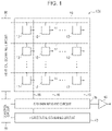
- FIG. 1 is a block diagram illustrating, in outline, the configuration of a solid-state image capturing apparatus according to the present embodiment, which is an example of a photoelectric conversion apparatus.
- FIG. 2 is an equivalent circuit schematic of a pixel of the solid-state image capturing apparatus according to the present embodiment.
- FIG. 3 is a diagram of a pixel of the solid-state image capturing apparatus according to the present embodiment illustrating the planar layout thereof.
- FIGS. 4A and 4B are schematic cross-sectional views of pixels of the solid-state image capturing apparatus according to the present embodiment.
- FIGS. 5A to 5C are cross-sectional views of pixels of a solid-state image capturing apparatus of a comparative example of the present embodiment.
- a solid-state image capturing apparatus 100 of the present embodiment includes a pixel region 10 , a vertical scanning circuit 20 , a column reading circuit 30 , a horizontal scanning circuit 40 , a control circuit 50 , and an output circuit 60 .
- the pixel region 10 includes a plurality of pixels 12 arrayed in rows and columns in a matrix pattern.
- a control signal line 14 extending in the row direction (in the lateral direction in FIG. 1 ) is disposed for each row of the pixel array of the pixel region 10 .
- the control signal line 14 is connected to the pixels 12 arranged in the row direction to form a signal line common to these pixels 12 .
- a vertical output line 16 extending in the column direction (in the vertical direction in FIG. 1 ) is disposed for each column of the pixel array of the pixel region 10 .
- the vertical output line 16 is connected to the pixels 12 arranged in the column direction to form a signal line common to these pixels 12 .
- the control signal line 14 of each row is connected to the vertical scanning circuit 20 .
- the vertical scanning circuit 20 is a circuit unit that supplies a control signal for driving a readout circuit in each pixel 12 to the pixel 12 through the control signal line 14 in reading a pixel signal from the pixel 12 .
- One end of the vertical output line 16 of each column is connected to the column reading circuit 30 .
- the pixel signal read from the pixel 12 is input to the column reading circuit 30 through the vertical output line 16 .
- the column reading circuit 30 is a circuit unit that performs predetermined signal processing, for example, amplification processing or analog-to-digital (AD) conversion processing, on the pixel signal read from the pixel 12 .
- the column reading circuit 30 can include a differential amplifier circuit, a sample and hold circuit, and an AD conversion circuit.
- the horizontal scanning circuit 40 is a circuit unit that supplies control signals for transferring the pixel signals processed in the column reading circuit 30 to the output circuit 60 in sequence to the column reading circuit 30 .
- the control circuit 50 is a circuit unit for supplying control signals for controlling the operations and their timings of the vertical scanning circuit 20 , the column reading circuit 30 , and the horizontal scanning circuit 40 .
- the output circuit 60 is a circuit unit including a buffer amplifier and a differential amplifier and used to output pixel signals read from the column reading circuit 30 to a signal processing device outside the solid-state image capturing apparatus 100 .
- each pixel 12 includes a photoelectric conversion unit PD, a transfer transistor M 1 , a reset transistor M 2 , an amplifying transistor M 3 , and a selection transistor M 4 .
- An example of the photoelectric conversion unit PD is a photodiode, whose anode is connected to a ground voltage line and whose cathode is connected to the source of the transfer transistor M 1 .
- the drain of the transfer transistor M 1 is connected to the source of the reset transistor M 2 and the gate of the amplifying transistor M 3 .
- the connection node of the drain of the transfer transistor M 1 , the source of the reset transistor M 2 , and the gate of the amplifying transistor M 3 is a what-is-called floating diffusion (FD) and constitutes a charge-voltage conversion unit composed of the capacitive component of the node.
- the drain of the reset transistor M 2 and the drain of the amplifying transistor M 3 are connected to a source voltage line (Vdd).
- the source of the amplifying transistor M 3 is connected to the drain of the selection transistor M 4 .
- the source of the selection transistor M 4 is connected to the vertical output line 16 .
- the other end of the vertical output line 16 A is connected to a current source 18 .
- the control signal line 14 includes a transfer-gate signal line TX, a reset signal line RES, and a selection signal line SEL.
- the transfer-gate signal line TX is connected to the gate of the transfer transistor M 1 .
- the reset signal line RES is connected to the gate of the reset transistor M 2 .
- the selection signal line SEL is connected to the gate of the selection transistor M 4 .
- the photoelectric conversion unit PD converts incident light to an amount of charges corresponding to the amount of the light (photoelectric conversion) and accumulates the generated charges.
- the transfer transistor M 1 transfers the charges of the photoelectric conversion unit PD to the floating diffusion FD.
- the floating diffusion FD goes to a voltage corresponding to the amount of charges transferred from the photoelectric conversion unit PD by charge-to-voltage conversion according to its capacitance.
- the amplifying transistor M 3 constitutes an amplifier (source follower circuit) with a configuration in which the drain is supplied with a power supply voltage Vdd, the source is supplied with a bias current from the current source 18 via the selection transistor M 4 , and the gate serves as an input node.
- the amplifying transistor M 3 outputs a signal based on the voltage of the floating diffusion PD to the vertical output line 16 via the selection transistor M 4 .
- the reset transistor M 2 Upon being turned on, the reset transistor M 2 resets the floating diffusion FD to a voltage according to the power supply voltage Vdd.
- FIG. 3 is a schematic diagram of the pixel 12 of the present embodiment illustrating a planar layout viewed from the top (incident plane).
- a front electrode 31 is an electrode used to apply an electric potential to a P-type isolation region 35 .
- the P-type isolation region 35 is disposed around the outer periphery of the photoelectric conversion unit PD.
- a transfer gate 21 is provided as part of the transfer transistor M 1 that transfers the charges of the photoelectric conversion unit PD.
- the transfer gate 21 is disposed between a floating diffusion region 23 , which is part of the floating diffusion (FD), and the photoelectric conversion unit PD.
- the transfer gate 21 is connected to the transfer-gate signal line TX.
- the floating diffusion region 23 is connected to an amplifying gate 25 , which is the gate of the amplifying transistor M 3 , through a PD connecting line.
- a selection gate 27 which is the gate of the selection transistor M 4 , is connected to a selection signal line SEL.
- One of the source and the drain of the selection transistor M 4 is connected to a signal line vout which is a vertical output line 16 .
- the other of the source and the drain of the selection transistor M 4 also serves as the source of the amplifying transistor M 3 .
- the drain of the amplifying transistor M 3 receives the power supply voltage Vdd.
- a reset gate 29 which is the gate of the reset transistor M 2 , is connected to a reset signal line RES.
- the drain of the reset transistor M 2 also serves as the drain of the amplifying transistor M 3 .
- the source of the reset transistor M 2 is connected to the floating diffusion region 23 and the amplifying gate 25 through the FD connecting line.
- FIG. 4A is a cross-sectional view of two pixels taken along line IVA-IVA of FIG. 3 .
- the same components as those of FIGS. 1 to 3 are denoted by the same reference signs as the signs in FIGS. 1 to 3 .
- a gate insulator film 11 is provided on a first surface of the semiconductor substrate.
- the gate insulator film 11 is typically composed of silicon oxide.
- the photoelectric conversion unit PD includes a P-type semiconductor region 42 and an N-type semiconductor region 44 .
- the N-type semiconductor region 44 is a charge accumulation region where electric charges generated by photoelectric conversion (in the present embodiment, electrons) are accumulated.
- a P-type semiconductor region 48 is provided under the N-type semiconductor region 44 .
- the P-type semiconductor region 42 is provided in contact with the first surface.
- the P-type semiconductor region 42 suppresses the inflow of charges generated due to a dark current generated on the surface of the semiconductor substrate into the N-type semiconductor region 44 .
- An N-type semiconductor region 46 serves as the floating diffusion region 23 illustrated in FIG. 3 .
- the P-type isolation region 35 disposed around the outer periphery of the photoelectric conversion unit PD is a P-type isolation region 41 in FIG. 4A .
- the P-type isolation region 41 is connected to the front electrode 31 .
- a back electrode 52 is provided under a second surface of the semiconductor substrate.
- the back electrode 52 is in contact with the P-type semiconductor region 48 .
- the back electrode 52 is disposed across the plurality of pixels 12 .
- the back electrode 52 is disposed across the pixel region 10 illustrated in FIG. 1 .
- this example is given merely for illustrative purposes.
- the back electrode 52 may be segmented for each pixel row.
- the back electrode 52 may be segmented for each pixel column.
- the back electrode 52 may also be segmented for each block including multiple rows and columns of pixels 12 .
- the N-type semiconductor region 44 (bottom) is disposed at a depth d 1 from the first surface of the semiconductor substrate.
- the depth of a semiconductor region is defined as the distance from the first face to the second face of that semiconductor region.
- a depth is deeper than another depth when its distance is longer than the distance of the other depth.
- a depth is shallower than another depth when its distance is shorter than the distance of the other depth.
- the P-type semiconductor region 48 (bottom) is disposed at a depth d 3 deeper than the depth d 1 .
- the P-type isolation region 41 is disposed so as to extend at least from the first depth d 1 to a depth d 2 shallower than the depth d 3 in the depth direction.
- the front electrode 31 receives a lower potential for the electrons serving as the carrier of the N-type semiconductor region 44 .
- the electric potential of the front electrode 31 is set at 0 V
- the electric potential of the back electrode 52 is set at ⁇ 10 V.
- the impurity concentration of the P-type semiconductor region 48 is lower than the impurity concentration of the P-type semiconductor region 42 .
- the impurity concentration of the P-type semiconductor region 48 is set at 1 ⁇ 10 11 [atom/cm 3 ]. This example is not intended to limit the present disclosure.
- the impurity concentration is lower than or equal to 1 ⁇ 10 12 [atom/cm 3 ].
- the impurity concentration of the P-type semiconductor region 48 is preferably 1 ⁇ 10 9 [atom/cm 3 ] or more to provide the function of the P-type semiconductor.
- the electrical resistivity of the P-type semiconductor region 48 is set to a high electrical resistivity of 3,000 [ ⁇ cm] or more.
- the electrical resistivity of the P-type semiconductor region 48 is preferably 300,000 [ ⁇ cm] or less corresponding to the lower limit impurity concentration at which the P-type semiconductor region 48 functions as a P-type semiconductor region.
- the impurity concentration of the P-type semiconductor region 42 is set at 2 ⁇ 10 19 [atom/cm 3 ].
- the impurity concentration is the concentration of impurities present in the semiconductor region.
- FIG. 4B is a schematic diagram illustrating equipotential lines for illustrating an electric potential distribution in the configuration of FIG. 4A .
- the front electrode 31 and the back electrode 52 are conducting through the P-type isolation region 41 and the P-type semiconductor region 48 , allowing a hole current 17 to flow therethrough.
- the P-type semiconductor region 48 has an the impurity concentration of 1 ⁇ 10 11 [atom/cm 3 ], as described above.
- the electrical resistance between the front electrode 31 and the back electrode 52 is high, causing an electric potential gradient in the P-type semiconductor region 48 .
- the electric potential gradient makes it easy for electrons 19 generated in the P-type semiconductor region 48 by the photoelectric conversion of incident light to move to the N-type semiconductor region 44 .
- the increase in electrons 19 collected to the N-type semiconductor region 44 enhances the sensitivity of the photoelectric conversion apparatus.
- the N-type semiconductor region 44 , the P-type semiconductor region 48 , and the P-type semiconductor region 42 form a depletion layer.
- the P-type isolation region 41 may extend to a position deeper than the N-type semiconductor region 44 .
- the P-type isolation region 41 may extend to a portion deeper than the depletion layer formed by the N-type semiconductor region 44 , the P-type semiconductor region 48 , and the P-type semiconductor region 42 .
- FIG. 5A illustrates a configuration in which a P-type isolation region 53 extends to the depth d 1 which is the same as the depth of the bottom of an N-type semiconductor region 56 .
- the P-type isolation region 53 receive a voltage of 0 V through the front electrode 31 , as in FIG. 4A .
- the N-type semiconductor region 56 is a charge accumulation layer, which is disposed under a P-type semiconductor region 54 .
- An N-type semiconductor region 62 is the floating diffusion region 23 .
- the back electrode 52 receives a voltage of ⁇ 10 V applied.
- FIG. 5B is a schematic diagram illustrating equipotential lines for illustrating an electric potential distribution in the configuration of FIG. 5A .
- the P-type isolation region 53 extends only to the depth d 1 , causing the depletion layers 55 of the adjacent pixels to connect to each other, as illustrated in FIG. 5B .
- FIG. 5C A electric potential distribution in this case is illustrated in FIG. 5C .
- the depletion layers 55 are high resistance regions where the hole current 17 between the P-type isolation region 53 and the back electrode 52 does not flow easily.
- the P-type semiconductor region 48 in FIG. 5C has electric potential gradients concentrated around the depth d 1 , although the P-type semiconductor region 48 in FIG. 4B has electric potential gradients in the area from the depth d 2 to the depth d 3 .
- the electric potential gradient in the area between the depth d 2 and the depth d 3 is small. This decreases the driving force for moving the electrons generated in the P-type semiconductor region 48 to the N-type semiconductor region 56 .
- This causes electrons generated in the P-type semiconductor region 48 of one pixel to be collected in the N-type semiconductor region 56 of another pixel, so-called crosstalk.
- the P-type isolation region 41 of the photoelectric conversion apparatus of the present embodiment extends to a position deeper than the N-type semiconductor region 44 , as illustrated in FIG. 4A . This makes it easy for the electrons 18 generated in the P-type semiconductor region 48 to move to the N-type semiconductor region 44 , as described above. This increases electrons 18 collected in the N-type semiconductor region 44 , improving the sensitivity of the photoelectric conversion apparatus.
- the impurity concentration of the P-type isolation region 41 may be higher than the impurity concentration of at least the P-type semiconductor region 48 .
- the increase in the impurity concentration of the P-type isolation region 41 decreases the electrical resistance to the hole current. This may also suppress depletion of the P-type isolation region 41 due to the electric potential difference from the N-type semiconductor region 44 .
- the electric potential difference in the P-type isolation region 41 may be smaller than the electric potential difference in the P-type semiconductor region 48 . This allows most of the electric potential difference between the front electrode 31 and the back electrode 52 to be formed in forming electric potential gradients in the P-type semiconductor region 48 , further reducing crosstalk.
- the photoelectric conversion unit PD includes a P-type semiconductor region PDS with a higher impurity concentration than the impurity concentration of the P-type semiconductor region 48 under the N-type semiconductor region 44 where signal charges are to be accumulated. This makes the capacitance of the depletion layer generated between the N-type semiconductor region 44 and the P-type semiconductor region PDS disposed thereunder larger than the capacitance of the first embodiment. Thus, the saturation charge amount of the photoelectric conversion unit PD is increased from the first embodiment.
- the P-type semiconductor region PDS is provided at a position overlapping with the photoelectric conversion unit PD in plan view, as illustrated in FIG. 6 .
- the P-type semiconductor region PDS has a higher impurity concentration than the impurity concentration of the P-type semiconductor region 48 .
- FIG. 7A is a cross-sectional view of a region taken along line VIIA-VIIA in FIG. 6 .
- the P-type semiconductor region PDS is disposed under the N-type semiconductor region 44 so as to be in contact with the bottom of the N-type semiconductor region 44 . Therefore, the N-type semiconductor region 44 and the P-type semiconductor region PDS form a PN junction.
- the depletion layer generated between the N-type semiconductor region 44 and the P-type semiconductor region PDS less expands than the depletion layer generated between the N-type semiconductor region 44 and the P-type semiconductor region 48 in the first embodiment.
- the capacitance of the depletion layer generated in the present embodiment is larger than the capacitance of the depletion layer generated in the first embodiment.
- the saturation charge amount of the photoelectric conversion unit PD is larger than the saturation charge amount of the first embodiment.
- the P-type semiconductor region PDS has slits so as to be divided, as illustrated in FIG. 6 and FIG. 7A .
- the signal charges (electrons) 18 generated in the P-type semiconductor region 48 move to the N-type semiconductor region 44 through the slits of the P-type semiconductor region PDS, as illustrated in FIG. 7B .
- the slits make it easy for the signal charges (electrons) 18 generated in the P-type semiconductor region 48 to move to the N-type semiconductor region 44 . This may improve the sensitivity to light with a wavelength that generates signal charges in the P-type semiconductor region 48 (typically, near infrared light and infrared light).
- the P-type semiconductor region PDS with a higher impurity concentration than the impurity concentration of the P-type semiconductor region 48 and the N-type semiconductor region 44 are joined together to form a PN junction. This increases the saturation charge amount of the photoelectric conversion unit PD.
- the slits in P-type semiconductor region PDS improve the sensitivity of the photoelectric conversion unit PD.
- a photoelectric conversion apparatus of the present embodiment will be described with a focus on differences from the first embodiment.
- FIG. 8 is a cross-sectional view of pixels of the photoelectric conversion apparatus of the present embodiment.
- the layout seen from the top may be the same as the layout of the first embodiment.
- the present embodiment is a what-is-called front-illuminated photoelectric conversion apparatus that receives light from the first surface of the semiconductor substrate.
- the photoelectric conversion apparatus of the present embodiment includes a reflection member 63 under the second surface of the semiconductor substrate.
- the reflection member 63 may be typically made of metal, such as aluminum, silver, or copper. The use of the reflection member 63 allows light passing through the P-type semiconductor region 48 to be reflected into the P-type semiconductor region 48 . This can further improve the sensitivity of the photoelectric conversion unit PD.
- the reflection member 63 can be omitted by using the back electrode 52 as a reflection member.
- a photoelectric conversion apparatus of the present embodiment will be described with a focus on differences from the first embodiment.
- FIG. 9 is a cross-sectional view of pixels of the photoelectric conversion apparatus of the present embodiment.
- the layout seen from the top may be the same as the layout of the first embodiment.
- the present embodiment is a what-is-called back-illuminated photoelectric conversion apparatus that receives light from the second surface of the semiconductor substrate.
- the back electrode 52 is a transparent electrode.
- the material of the transparent electrode may be indium oxide, tin oxide, titanium oxide, graphene, or a mixture thereof.
- An antireflection film 64 is disposed under the back electrode 52 (light incident side). This suppresses reflection of incident light from the back electrode 52 . This can improve the sensitivity of the photoelectric conversion unit PD.
- the antireflection film 64 may be a single layer or a plurality of layers with different refractive indices.
- a photoelectric conversion apparatus of the present embodiment will be described with a focus on differences from the first embodiment.
- the photoelectric conversion apparatus of the present embodiment has a configuration in which one pixel includes one microlens and a plurality of photoelectric conversion units PD that receive light passing through the one microlens.
- the photoelectric conversion apparatus with this configuration can output signals for use in focus detection of a phase-difference detection method.
- FIG. 10A is a top view of a pixel of the present embodiment.
- components having the same functions as the functions of the components of the first embodiment described in FIG. 3 are denoted by the same reference signs as the signs of FIG. 3 .
- the pixels of the present embodiment each have a plurality of photoelectric conversion units PD 1 and PD 2 .
- the pixel includes a transfer gate 21 a corresponding to the photoelectric conversion unit PD 1 and a transfer gate 21 b corresponding to the photoelectric conversion unit PD 2 .
- the transfer gates 21 a and 21 b share the floating diffusion region 23 .
- the transfer gate 21 a is connected to a transfer-gate signal line TX 1 .
- the transfer gate 21 b is connected to a transfer-gate signal line TX 2 .
- FIG. 10B is a cross-sectional view taken along line XB-XB in FIG. 10A .
- the P-type isolation region 41 is disposed at positions where the plurality of pixels are separated and a position where a region of the photoelectric conversion unit PD and a region of transistors are disposed are separated.
- the region of the transistors is a region in which an amplifying transistor, a reset transistor, and a selection transistor are disposed.
- the P-type isolation region 41 is not disposed between the photoelectric conversion unit PD 1 and the photoelectric conversion unit PD 2 .
- FIGS. 10A and 10B may be used in the front-illuminated photoelectric conversion apparatus of the third embodiment.
- the configuration may also be used in a photoelectric conversion apparatus that uses photoelectric conversion of, for example, visible light with wavelengths shorter than the wavelengths of near infrared light. This is because the light with wavelengths in the visible light range is converted to electric signals in the vicinity of the surfaces of the photoelectric conversion units PD 1 and PD 2 , and signal charges are accumulated in the respective N-type semiconductor regions 44 a and 44 b of the photoelectric conversion units PD 1 and PD 2 according to the incident positions.
- FIGS. 11A and 11B are diagrams illustrating another layout of the P-type isolation regions 41 .
- components having the same functions as the functions of the components described in FIGS. 10A and 10B are denoted by the same reference signs as the signs of FIGS. 10A and 10B .
- the P-type isolation region 41 is disposed between the photoelectric conversion unit PD 1 and the photoelectric conversion unit PD 2 , in addition to the P-type isolation region 41 illustrated in FIGS. 10A and 10B .
- FIG. 11B is a cross-sectional view taken along XIB-XIB in FIG. 11A .
- the P-type isolation region 41 is disposed between the N-type semiconductor region 44 a and the N-type semiconductor region 44 b .
- the P-type isolation region 41 extends from the bottom of the P-type semiconductor region 42 to a depth deeper than the bottoms of the N-type semiconductor regions 44 a and 44 b.
- FIGS. 11A and 11B may be used in both of front-illuminated and back-illuminated photoelectric conversion apparatuses.
- crosstalk between electric charges generated in and in the vicinity of the photoelectric conversion unit PD 1 and electric charges generated in and in the vicinity of the photoelectric conversion unit PD 2 can be reduced.
- the P-type isolation region 41 is disposed between the photoelectric conversion unit PD 1 and the photoelectric conversion unit PD 2 , in addition to the P-type isolation region 41 illustrated in FIGS. 10A and 10B , as in FIGS. 11A and 11B .
- FIG. 12B is a cross-sectional view taken along XIIB-XIIB in FIG. 12A .
- the P-type isolation region 41 extends from the bottom of the P-type semiconductor region 42 to a depth deeper than the bottoms of the N-type semiconductor regions 44 a and 44 b .
- the P-type isolation region 41 extends from a position deeper than the bottom of the P-type semiconductor region 42 to a depth deeper than the bottoms of the N-type semiconductor regions 44 a and 44 b.
- the configuration illustrated in FIGS. 12A and 12B may be used in both of front-illuminated and back-illuminated photoelectric conversion apparatuses.
- both of the photoelectric conversion apparatuses if one of the photoelectric conversion units PD 1 and PD 2 is saturated, the signal charges overflow not to the photoelectric conversion unit PD 1 or PD 2 of another pixel but to another of the photoelectric conversion units PD 1 and PD 2 of the same pixel.
- adjacent pixels may have color filters of different colors.
- FIGS. 13A to 13D A configuration illustrated in FIGS. 7A and 7B is an application of the configuration of FIGS. 7A and 7B .
- FIG. 13B is a cross-sectional view taken along line XIIIB-XIIIB in FIG. 13A .
- FIG. 13C is a cross-sectional view taken along line XIIIC-XIIIC in FIG. 13A .
- FIG. 13D is a cross-sectional view taken along line XIIID-XIIID in FIG. 13A .
- the photoelectric conversion apparatus of the present embodiment also has the P-type semiconductor region PDS under the bottoms of the N-type semiconductor regions 44 a and 44 b . This can increase the saturation charges of the photoelectric conversion units PD 1 and PD 2 .
- a photoelectric conversion apparatus of the present embodiment will be described with a focus on differences from the first embodiment.
- FIGS. 14A and 14B are top views of a pixel of the photoelectric conversion apparatus of the present embodiment.
- components having the same functions as the functions of the components described in FIG. 3 are denoted by the same reference signs as the signs of FIG. 3 .
- the photoelectric conversion apparatus of the present embodiment includes an insulating member 71 in the P-type isolation region 41 .
- the insulating member 71 may be made of silicon oxide, silicon nitride, silicon oxynitride, or the like.
- the front electrode 31 is connected to the P-type isolation region 41 .
- the insulating member 71 is coated with the P-type isolation region 41 . This can prevent dark current generated because of the insulating member 71 from flowing to the N-type semiconductor region 44 .
- Providing the insulating member 71 allows the width of the region isolating the pixels from each other to be smaller than the width in the first embodiment. This allows increasing the number of pixels of the pixel array and miniaturizing the pixels.
- a photoelectric conversion apparatus of the present embodiment will be described with a focus on differences from the first embodiment.
- the front electrode (a well contact 81 ) is shared by a plurality of pixels.
- FIG. 15 is a top view of the photoelectric conversion apparatus of the present embodiment.
- components having the same functions as the functions of the components described in FIG. 3 are denoted by the same reference signs as the signs of FIG. 3 .
- the well contact 81 that conducts electricity between the front electrode 31 and the P-type isolation region 41 is provided for each of a plurality of rows and columns of pixels. In the example of FIG. 15 , one well contact 81 is provided for four pixels in two rows and two columns.
- the well contact 81 may be provided for each pixel.
- an increase in the number of well contacts 81 increases the pixel pitch, hindering increasing the number of pixels of the pixel array and miniaturizing the pixels.
- the area of the photoelectric conversion unit PD has to be small, which may decrease the sensitivity.
- the well contact 81 may be shared by a plurality of pixels within a range that allows a decrease in electrical resistance between the back electrode 52 and the front electrode 31 .
- the photoelectric conversion apparatus of the present embodiment is easy to increase in the number of pixels of the pixel array and miniaturize the pixels by sharing the well contact 81 among a plurality of pixels. Furthermore, the configuration of the photoelectric conversion apparatus of the present embodiment can suppress a decrease in the area of the photoelectric conversion unit PD, reducing pre eliminating a decrease in sensitivity.
- a photoelectric conversion apparatus of the present embodiment will be described with a focus on differences from the first embodiment.
- the layout of the photoelectric conversion apparatus of the present embodiment seen from the top may be the same as the layout in FIG. 3 .
- FIG. 16 is a cross-sectional view taken along line XVI-XVI in FIG. 3 .
- components having the same functions as the functions of the components described in FIGS. 4A and 4B are denoted by the same reference signs as the signs of FIGS. 4A and 4B .
- the present embodiment includes a P-type semiconductor region 91 on the back electrode 52 .
- the P-type semiconductor region 91 has a higher impurity concentration than the P-type semiconductor region 48 .
- the P-type semiconductor region 91 has an impurity concentration similar to the impurity concentration of the P-type isolation region 41 .
- an electronic current due to electrons injected through the back electrode 52 flows between the P-type isolation region 41 and the back electrode 52 in response to a hole current flowing therethrough.
- the electrons due to the electronic current if entering the N-type semiconductor region 44 , cause noise. This noise is noticeable if the light incident on the photoelectric conversion unit PD is low (that is, low light).
- the P-type semiconductor region 91 is disposed on the back electrode 52 . This configuration allows the electrons injected through the back electrode 52 is offset by the holes of the P-type semiconductor region 91 . This suppresses unnecessary injection of electrons into the N-type semiconductor region 44 , thus reducing noise.
- the photoelectric conversion apparatus of the present embodiment includes the P-type semiconductor region 91 on the back electrode 52 to suppress unnecessary injection of electric charges into the N-type semiconductor region 44 through the back electrode 52 , thereby reducing noise.
- a photoelectric conversion apparatus of the present embodiment will be described with a focus on differences from the first embodiment.
- the photoelectric conversion apparatus of the present embodiment forms electric potential gradients in the P-type semiconductor region 48 without using a back electrode.
- FIG. 17 is a cross-sectional view taken along line XVII-XVII in FIG. 3 .
- components having the same functions as the functions of the components described in FIGS. 4A and 4B are denoted by the same reference signs as the signs of FIGS. 4A and 4B .
- the present embodiment includes a P-type semiconductor region 98 under the bottom of the P-type semiconductor region 48 .
- the impurity concentration of the P-type semiconductor region 98 is set higher than the impurity concentration of the P-type semiconductor region 48 .
- the P-type semiconductor region 98 is disposed along the second surface of the semiconductor substrate so as to be in contact with the second surface.
- a P-type isolation region 96 extends from the first surface of the semiconductor substrate in the depth direction to the P-type semiconductor region 98 .
- the P-type isolation region 96 and the P-type semiconductor region 98 may have similar impurity concentrations.
- the P-type isolation region 96 is connected to a front electrode 93 .
- the voltage applied through the front electrode 93 may be the same as the voltage applied by the back electrode 52 of the first embodiment.
- This configuration includes an N-type semiconductor region 97 serving as a guardring to reduce the current flowing due to the voltage difference between the P-type isolation region 96 and the P-type isolation region 41 .
- the N-type semiconductor region 97 receives a predetermined electric potential through a front electrode 95 .
- the N-type semiconductor region 97 receives an intermediate electric potential between the electric potential of the P-type isolation region 96 and the electric potential of the P-type isolation region 41 . This reduces the current to flow between the P-type isolation region 96 and the P-type isolation region 41 .
- the present embodiment can form the electric potential gradients in the P-type semiconductor region 48 without a back electrode. Furthermore, providing the guardring reduces the current to flow between the P-type isolation region 96 and the P-type isolation region 41 .
- a photoelectric conversion apparatus of the present embodiment will be described with a focus on differences from the first embodiment.
- the photoelectric conversion apparatus of the present embodiment includes pixels for receiving visible light and pixels for receiving near infrared light and/or infrared light with longer wavelengths than the wavelengths of visible light.
- FIG. 18 is a cross-sectional view of the photoelectric conversion apparatus of the present embodiment.
- components having the same functions as the functions of the components described in FIGS. 4A and 4B are denoted by the same reference signs as the signs of FIGS. 4A and 4B .
- a pixel P 27 is a pixel for receiving visible light.
- a pixel P 28 is a pixel for receiving light with longer wavelengths than the wavelengths of visible light.
- the pixel P 27 includes a P-type semiconductor region 181 under the bottom of the N-type semiconductor region 44 .
- the impurity concentration of the P-type semiconductor region 181 may be similar to the impurity concentration of the P-type semiconductor region 41 .
- a P-type isolation region 99 is disposed so as to surround the P-type semiconductor region 181 .
- the P-type isolation region 99 receives a predetermined electric potential through a front electrode 101 .
- the configuration of the pixel P 28 may be the same as the configuration of the first embodiment.
- the pixel P 27 includes the P-type isolation region 99 , electrons generated in the P-type semiconductor region 48 can be prevented from flowing into the N-type semiconductor region 44 of the pixel P 27 .
- FIG. 19 is a block diagram illustrating, in outline, the configuration of an image capturing system according to the present embodiment.
- the photoelectric conversion apparatuses of the above embodiments may be used as an image capturing apparatus 201 of FIG. 19 to various image capturing systems.
- Examples of applicable photoelectric conversion systems include digital still cameras, digital camcorders, monitoring cameras, copy machines, facsimile machines, mobile phones, car-mounted cameras, and observation satellites.
- Another example of the photoelectric conversion system is a camera module including an optical system, such as a lens, and an image capturing apparatus.
- FIG. 19 illustrates a block diagram of a digital still camera by way of example.
- An image capturing system 200 illustrated in FIG. 19 includes the image capturing apparatus 201 , a lens 202 for forming an optical image of the subject on the image capturing apparatus 201 , an aperture 204 for varying the amount of light passing through the lens 202 , and a barrier 206 for protecting the lens 202 .
- the lens 202 and the aperture 204 constitute an optical system that collects light to the image capturing apparatus 201 .
- the image capturing system 200 further includes a signal processing unit 208 that processes a signal output from the image capturing apparatus 201 .
- the signal processing unit 208 performs analog-to-digital (AD) conversion for converting an analog signal output from the image capturing apparatus 201 to a digital signal.
- the signal processing unit 208 also performs various corrections and compressions as necessary and outputs image data.
- An AD conversion unit, which is part of the signal processing unit 208 may be disposed on a semiconductor substrate on which the image capturing apparatus 201 is disposed or on another semiconductor substrate separate from the image capturing apparatus 201 .
- the image capturing apparatus 201 and the signal processing unit 208 may be disposed on the same semiconductor substrate.
- the image capturing system 200 further includes a memory 210 for temporarily storing image data and an external interface (external I/F) 212 for communicating with an external computer or the like.
- the image capturing system 200 further includes a recording medium 214 , such as a semiconductor memory, for recording or reading captured data and a recording-medium control interface (recording-medium control I/F) 216 for recording or reading captured data to or from the recording medium 214 .
- the recording medium 214 may be provided in the image capturing system 200 or may be detachable.
- the image capturing system 200 further includes an overall control/calculation unit 218 that performs various calculations and controls the entire digital still camera and a timing generation unit 220 that outputs various timing signals to the image capturing apparatus 201 and the signal processing unit 208 .
- the timing signals may be input externally.
- the image capturing system 200 may include at least the image capturing apparatus 201 and the signal processing unit 208 that processes signals output from the image capturing apparatus 201 .
- the image capturing apparatus 201 outputs an image capture signal to the signal processing unit 208 .
- the signal processing unit 208 performs predetermined signal processing on the image capture signal output from the image capturing apparatus 201 and outputs image data.
- the signal processing unit 208 generates an image using the image capture signal.
- the use of the photoelectric conversion apparatuses according to the above embodiments as the image capturing apparatus 201 provides an image capturing system and a photoelectric conversion system capable of stably capturing high-quality images with high sensitivity and a large amount of saturation signals.
- FIGS. 20A and 20B are diagrams illustrating the configurations of an image capturing system and a moving object according to the present embodiment, respectively.
- FIG. 20A illustrates an example of an image capturing system for a car-mounted camera.
- An image capturing system 300 includes an image capturing apparatus 310 .
- the image capturing apparatus 310 is the photoelectric conversion apparatus according to any one of the above embodiments.
- the image capturing system 300 further includes an image processing unit 312 that processes a plurality of image data obtained by the image capturing apparatus 310 and a disparity calculation unit 314 that calculates the disparity (the phase difference of the disparity images) from the plurality of image data obtained by the image capturing system 300 .
- the image capturing system 300 further includes a distance measuring unit 316 that calculates a distance to the object from the calculated disparity and a collision determination unit 318 that determines whether there is a possibility of a collision from the calculated distance.
- the disparity calculation unit 314 and the distance measuring unit 316 are examples of a distance-information acquisition unit for obtaining object-distance information.
- the distance information is information on a disparity, a defocus amount, the distance to the object, and so on.
- the collision determination unit 318 may determine whether there is a collision possibility using any of the distance information.
- the distance-information acquisition unit may be implemented by specifically designed hardware or a software module.
- the distance-information acquisition unit may also be implemented by a field programmable gate array (FPGA), an application specific integrated circuit (ASIC), or a combination thereof.
- FPGA field programmable gate array
- ASIC application specific integrated circuit
- the image capturing system 300 is connected to a vehicle-information acquisition apparatus 320 and can obtain vehicle information, such as a vehicle speed, a yaw rate, and a rudder angle.
- vehicle information such as a vehicle speed, a yaw rate, and a rudder angle.
- the image capturing system 300 is connected to an electronic control unit (ECU) 330 , which is a control unit that outputs a control signal for generating a braking force for the vehicle based on the determination result of the collision determination unit 318 .
- ECU electronice control unit
- the image capturing system 300 is also connected to a warning device 340 that gives a warning to the driver based on the determination result of the collision determination unit 318 .
- the ECU 330 performs vehicle control to avoid a collision by putting on the brake, releasing the accelerator, or suppressing engine output, to reduce damages.
- the warning device 340 gives a warning to the user by sounding an alarm, displaying warning information on the screen of a car navigation system or the like, or vibrating the seat belt or the steering wheel.
- the present embodiment captures images of the surroundings of the vehicle, for example, a forward image and a backward image, with the image capturing system 300 .
- FIG. 20B illustrates the image capturing system capturing an image in front of the vehicle (an image capture region 350 ).
- the vehicle-information acquisition apparatus 320 sends an instruction to perform a predetermined operation to the image capturing system 300 or the image capturing apparatus 310 . This configuration can further improve the accuracy of ranging.
- the image capturing system 300 may also be used in control to automatically follow another vehicle and control to automatically drive so as not to go out of the lane.
- the image capturing system may be used not only for vehicles, such as cars, but also for moving objects (moving apparatuses), such as ships, aircrafts, and industrial robots.
- moving objects moving apparatuses
- the image capturing system may be broadly used in object recognition apparatuses, such as an intelligent transport system (ITS).
- ITS intelligent transport system
- the disclosure includes an embodiment in which part of the configuration of any of the embodiments is added to another embodiment and an embodiment in which part of the configuration of any of the embodiments is replaced with part of the configuration of another embodiment.
- the disclosure can also be applied to a solid-state image capturing apparatus including a photoelectric conversion unit PD that generates holes as signal charges.
- the conductivity type of the semiconductor regions constituting the elements of the pixels are reversed.
Landscapes
- Engineering & Computer Science (AREA)
- Computer Vision & Pattern Recognition (AREA)
- Physics & Mathematics (AREA)
- General Physics & Mathematics (AREA)
- Theoretical Computer Science (AREA)
- Multimedia (AREA)
- Signal Processing (AREA)
- Solid State Image Pick-Up Elements (AREA)
- Transforming Light Signals Into Electric Signals (AREA)
- Light Receiving Elements (AREA)
Abstract
Description
Claims (25)
Applications Claiming Priority (3)
| Application Number | Priority Date | Filing Date | Title |
|---|---|---|---|
| JP2018224274A JP2020088291A (en) | 2018-11-29 | 2018-11-29 | Photoelectric conversion device, photoelectric conversion system, and moving body |
| JPJP2018-224274 | 2018-11-29 | ||
| JP2018-224274 | 2018-11-29 |
Publications (2)
| Publication Number | Publication Date |
|---|---|
| US20200176491A1 US20200176491A1 (en) | 2020-06-04 |
| US11393855B2 true US11393855B2 (en) | 2022-07-19 |
Family
ID=70848767
Family Applications (1)
| Application Number | Title | Priority Date | Filing Date |
|---|---|---|---|
| US16/693,114 Active 2040-02-07 US11393855B2 (en) | 2018-11-29 | 2019-11-22 | Photoelectric conversion apparatus, photoelectric conversion system, and moving object |
Country Status (2)
| Country | Link |
|---|---|
| US (1) | US11393855B2 (en) |
| JP (1) | JP2020088291A (en) |
Families Citing this family (1)
| Publication number | Priority date | Publication date | Assignee | Title |
|---|---|---|---|---|
| JP2020088291A (en) * | 2018-11-29 | 2020-06-04 | キヤノン株式会社 | Photoelectric conversion device, photoelectric conversion system, and moving body |
Citations (24)
| Publication number | Priority date | Publication date | Assignee | Title |
|---|---|---|---|---|
| US6576940B2 (en) * | 2000-07-21 | 2003-06-10 | Mitsubishi Denki Kabushiki Kaisha | Semiconductor device having a solid state image sensing device and manufacturing method thereof |
| US20060027844A1 (en) * | 2004-08-06 | 2006-02-09 | Samsung Electronics Co., Ltd. | Image sensor and method of manufacturing the same |
| US20060065896A1 (en) * | 2004-09-22 | 2006-03-30 | Hideshi Abe | CMOS solid-state imaging device and method of manufacturing the same as well as drive method of CMOS solid-state imaging device |
| US20090045321A1 (en) * | 2007-01-24 | 2009-02-19 | Jeong-Hoon Bae | Image sensor, method of manufacturing the same, and method of operating the same |
| JP2009038309A (en) | 2007-08-03 | 2009-02-19 | Sharp Corp | Solid-state imaging device, manufacturing method thereof, and electronic information device |
| JP2010056345A (en) | 2008-08-28 | 2010-03-11 | Brookman Technology Inc | Amplification type solid state imaging device |
| US20100066882A1 (en) | 2008-09-18 | 2010-03-18 | Sharp Kabushiki Kaisha | Solid-state image capturing element and electronic information device |
| US20100327391A1 (en) * | 2009-06-26 | 2010-12-30 | Mccarten John P | Back-illuminated image sensor with electrically biased frontside and backside |
| US20110298078A1 (en) | 2010-06-02 | 2011-12-08 | Sony Corporation | Method for production of solid-state imaging element, solid-state imaging element, and imaging apparatus |
| US20120295390A1 (en) * | 2011-05-20 | 2012-11-22 | International Business Machines Corporation | Single-crystalline silicon alkaline texturing with glycerol or ethylene glycol additives |
| US20120329200A1 (en) * | 2011-06-21 | 2012-12-27 | International Business Machines Corporation | Silicon surface texturing method for reducing surface reflectance |
| US20130025663A1 (en) * | 2011-07-27 | 2013-01-31 | International Business Machines Corporation | Inverted pyramid texture formation on single-crystalline silicon |
| US8471317B2 (en) * | 2001-07-11 | 2013-06-25 | Sony Corporation | X-Y address type solid state image pickup device and method of producing the same |
| US8546902B2 (en) * | 2004-05-06 | 2013-10-01 | Canon Kabushiki Kaisha | Photoelectric conversion device and manufacturing method thereof |
| US20140111664A1 (en) * | 2012-10-22 | 2014-04-24 | Canon Kabushiki Kaisha | Image capturing apparatus, manufacturing method thereof, and camera |
| US20150263058A1 (en) * | 2014-03-12 | 2015-09-17 | E2V Technologies (Uk) Limited | Cmos image sensor with backside biased substrate |
| US20170323912A1 (en) * | 2015-03-23 | 2017-11-09 | Tower Semiconductor Ltd. | Image Sensor Pixel With Memory Node Having Buried Channel And Diode Portions Formed On N-Type Substrate |
| US20180233540A1 (en) * | 2015-08-27 | 2018-08-16 | Sony Semiconductor Solutions Corporation | Photoelectric conversion element, imaging device, and electronic apparatus |
| US20200176491A1 (en) * | 2018-11-29 | 2020-06-04 | Canon Kabushiki Kaisha | Photoelectric conversion apparatus, photoelectric conversion system, and moving object |
| US20200176490A1 (en) * | 2018-11-29 | 2020-06-04 | Canon Kabushiki Kaisha | Photoelectric conversion device, photoelectric conversion system, and mobile apparatus |
| US10686086B2 (en) * | 2017-10-27 | 2020-06-16 | Canon Kabushiki Kaisha | Photoelectric conversion device, manufacturing method thereof, and apparatus |
| US20200258923A1 (en) * | 2017-08-16 | 2020-08-13 | Sony Corporation | Imaging element, laminated imaging element, and solid-state imaging device |
| US20200350346A1 (en) * | 2017-11-09 | 2020-11-05 | Sony Semiconductor Solutions Corporation | Solid-state imaging device and electronic apparatus |
| US20210151478A1 (en) * | 2018-03-20 | 2021-05-20 | Sony Semiconductor Solutions Corporation | Solid-state image pickup device, manufacturing method therefor, and electronic apparatus |
Family Cites Families (10)
| Publication number | Priority date | Publication date | Assignee | Title |
|---|---|---|---|---|
| JP2002057318A (en) * | 2000-08-07 | 2002-02-22 | Sony Corp | Solid-state imaging device and method of manufacturing the same |
| JP4123415B2 (en) * | 2002-05-20 | 2008-07-23 | ソニー株式会社 | Solid-state imaging device |
| CN100442530C (en) * | 2005-02-21 | 2008-12-10 | 索尼株式会社 | Solid-state imaging device, driving method thereof, and camera device |
| JP2006261638A (en) * | 2005-02-21 | 2006-09-28 | Sony Corp | Solid-state imaging device and driving method of solid-state imaging device |
| JP5368007B2 (en) * | 2008-05-15 | 2013-12-18 | 日本電信電話株式会社 | Photodetector array |
| JP2014165286A (en) * | 2013-02-23 | 2014-09-08 | Nikon Corp | Photodiode, solid state image sensor, and imaging apparatus |
| JP6302216B2 (en) * | 2013-11-08 | 2018-03-28 | ルネサスエレクトロニクス株式会社 | Semiconductor device and manufacturing method thereof |
| JP6123866B2 (en) * | 2015-10-26 | 2017-05-10 | ソニー株式会社 | Solid-state imaging device and electronic apparatus |
| JP2017157804A (en) * | 2016-03-04 | 2017-09-07 | キヤノン株式会社 | Imaging device |
| JP6985054B2 (en) * | 2017-08-01 | 2021-12-22 | スタンレー電気株式会社 | Imaging device |
-
2018
- 2018-11-29 JP JP2018224274A patent/JP2020088291A/en not_active Ceased
-
2019
- 2019-11-22 US US16/693,114 patent/US11393855B2/en active Active
Patent Citations (27)
| Publication number | Priority date | Publication date | Assignee | Title |
|---|---|---|---|---|
| US6576940B2 (en) * | 2000-07-21 | 2003-06-10 | Mitsubishi Denki Kabushiki Kaisha | Semiconductor device having a solid state image sensing device and manufacturing method thereof |
| US8471317B2 (en) * | 2001-07-11 | 2013-06-25 | Sony Corporation | X-Y address type solid state image pickup device and method of producing the same |
| US8546902B2 (en) * | 2004-05-06 | 2013-10-01 | Canon Kabushiki Kaisha | Photoelectric conversion device and manufacturing method thereof |
| US20060027844A1 (en) * | 2004-08-06 | 2006-02-09 | Samsung Electronics Co., Ltd. | Image sensor and method of manufacturing the same |
| US20060065896A1 (en) * | 2004-09-22 | 2006-03-30 | Hideshi Abe | CMOS solid-state imaging device and method of manufacturing the same as well as drive method of CMOS solid-state imaging device |
| US20090045321A1 (en) * | 2007-01-24 | 2009-02-19 | Jeong-Hoon Bae | Image sensor, method of manufacturing the same, and method of operating the same |
| JP2009038309A (en) | 2007-08-03 | 2009-02-19 | Sharp Corp | Solid-state imaging device, manufacturing method thereof, and electronic information device |
| US20090050997A1 (en) * | 2007-08-03 | 2009-02-26 | Sharp Kabushiki Kaisha | Solid-state image capturing device, manufacturing method for the solid-state image capturing device, and electronic information device |
| JP2010056345A (en) | 2008-08-28 | 2010-03-11 | Brookman Technology Inc | Amplification type solid state imaging device |
| JP2010073906A (en) | 2008-09-18 | 2010-04-02 | Sharp Corp | Solid-state imaging element, and electronic information apparatus |
| US20100066882A1 (en) | 2008-09-18 | 2010-03-18 | Sharp Kabushiki Kaisha | Solid-state image capturing element and electronic information device |
| US20100327391A1 (en) * | 2009-06-26 | 2010-12-30 | Mccarten John P | Back-illuminated image sensor with electrically biased frontside and backside |
| US20110298078A1 (en) | 2010-06-02 | 2011-12-08 | Sony Corporation | Method for production of solid-state imaging element, solid-state imaging element, and imaging apparatus |
| JP2011253963A (en) | 2010-06-02 | 2011-12-15 | Sony Corp | Method of manufacturing solid state image sensor, solid state image sensor, imaging apparatus |
| US20120295390A1 (en) * | 2011-05-20 | 2012-11-22 | International Business Machines Corporation | Single-crystalline silicon alkaline texturing with glycerol or ethylene glycol additives |
| US20120329200A1 (en) * | 2011-06-21 | 2012-12-27 | International Business Machines Corporation | Silicon surface texturing method for reducing surface reflectance |
| US20130025663A1 (en) * | 2011-07-27 | 2013-01-31 | International Business Machines Corporation | Inverted pyramid texture formation on single-crystalline silicon |
| US20140111664A1 (en) * | 2012-10-22 | 2014-04-24 | Canon Kabushiki Kaisha | Image capturing apparatus, manufacturing method thereof, and camera |
| US20150263058A1 (en) * | 2014-03-12 | 2015-09-17 | E2V Technologies (Uk) Limited | Cmos image sensor with backside biased substrate |
| US20170323912A1 (en) * | 2015-03-23 | 2017-11-09 | Tower Semiconductor Ltd. | Image Sensor Pixel With Memory Node Having Buried Channel And Diode Portions Formed On N-Type Substrate |
| US20180233540A1 (en) * | 2015-08-27 | 2018-08-16 | Sony Semiconductor Solutions Corporation | Photoelectric conversion element, imaging device, and electronic apparatus |
| US20200258923A1 (en) * | 2017-08-16 | 2020-08-13 | Sony Corporation | Imaging element, laminated imaging element, and solid-state imaging device |
| US10686086B2 (en) * | 2017-10-27 | 2020-06-16 | Canon Kabushiki Kaisha | Photoelectric conversion device, manufacturing method thereof, and apparatus |
| US20200350346A1 (en) * | 2017-11-09 | 2020-11-05 | Sony Semiconductor Solutions Corporation | Solid-state imaging device and electronic apparatus |
| US20210151478A1 (en) * | 2018-03-20 | 2021-05-20 | Sony Semiconductor Solutions Corporation | Solid-state image pickup device, manufacturing method therefor, and electronic apparatus |
| US20200176491A1 (en) * | 2018-11-29 | 2020-06-04 | Canon Kabushiki Kaisha | Photoelectric conversion apparatus, photoelectric conversion system, and moving object |
| US20200176490A1 (en) * | 2018-11-29 | 2020-06-04 | Canon Kabushiki Kaisha | Photoelectric conversion device, photoelectric conversion system, and mobile apparatus |
Also Published As
| Publication number | Publication date |
|---|---|
| US20200176491A1 (en) | 2020-06-04 |
| JP2020088291A (en) | 2020-06-04 |
Similar Documents
| Publication | Publication Date | Title |
|---|---|---|
| US11553149B2 (en) | Solid-state imaging device, imaging system and movable object | |
| US10453879B2 (en) | Solid-state imaging device, imaging system, and movable object | |
| US10868069B2 (en) | Solid state imaging device, imaging system, and mobile apparatus | |
| CN110931517B (en) | Light detection device | |
| US10381388B2 (en) | Solid-state imaging device and imaging system | |
| US11348961B2 (en) | Photoelectric conversion apparatus, photoelectric conversion system, and movable object | |
| US20200176490A1 (en) | Photoelectric conversion device, photoelectric conversion system, and mobile apparatus | |
| US11393855B2 (en) | Photoelectric conversion apparatus, photoelectric conversion system, and moving object | |
| US12068342B2 (en) | Photoelectric conversion device, imaging system, and movable body | |
| US12272710B2 (en) | Semiconductor device and equipment | |
| US11431922B2 (en) | Photoelectric conversion apparatus, imaging system, and moving object, with high sensitivity and saturation charge | |
| US11575822B2 (en) | Photoelectric conversion apparatus, photoelectric conversion system, and moving body | |
| US12176358B2 (en) | Photoelectric conversion apparatus, photoelectric conversion system, and moving body | |
| JP6946379B2 (en) | Solid-state image sensor and image sensor | |
| JP2020096147A (en) | Photoelectric conversion device, photoelectric conversion system, moving body | |
| JP2023174479A (en) | Photoelectric conversion device | |
| JP2020107915A (en) | Solid-state imaging apparatus and imaging system |
Legal Events
| Date | Code | Title | Description |
|---|---|---|---|
| FEPP | Fee payment procedure |
Free format text: ENTITY STATUS SET TO UNDISCOUNTED (ORIGINAL EVENT CODE: BIG.); ENTITY STATUS OF PATENT OWNER: LARGE ENTITY |
|
| STPP | Information on status: patent application and granting procedure in general |
Free format text: NON FINAL ACTION MAILED |
|
| STPP | Information on status: patent application and granting procedure in general |
Free format text: RESPONSE TO NON-FINAL OFFICE ACTION ENTERED AND FORWARDED TO EXAMINER |
|
| STPP | Information on status: patent application and granting procedure in general |
Free format text: NON FINAL ACTION MAILED |
|
| STPP | Information on status: patent application and granting procedure in general |
Free format text: NON FINAL ACTION MAILED |
|
| STPP | Information on status: patent application and granting procedure in general |
Free format text: RESPONSE TO NON-FINAL OFFICE ACTION ENTERED AND FORWARDED TO EXAMINER |
|
| STPP | Information on status: patent application and granting procedure in general |
Free format text: NOTICE OF ALLOWANCE MAILED -- APPLICATION RECEIVED IN OFFICE OF PUBLICATIONS |
|
| STPP | Information on status: patent application and granting procedure in general |
Free format text: PUBLICATIONS -- ISSUE FEE PAYMENT RECEIVED |
|
| STCF | Information on status: patent grant |
Free format text: PATENTED CASE |
|
| AS | Assignment |
Owner name: CANON KABUSHIKI KAISHA, JAPAN Free format text: ASSIGNMENT OF ASSIGNORS INTEREST;ASSIGNORS:IKEDA, HAJIME;ONUKI, YUSUKE;SIGNING DATES FROM 20191114 TO 20191115;REEL/FRAME:063848/0159 |