US11391992B2 - Liquid crystal display and manufacturing method thereof - Google Patents
Liquid crystal display and manufacturing method thereof Download PDFInfo
- Publication number
- US11391992B2 US11391992B2 US15/981,032 US201815981032A US11391992B2 US 11391992 B2 US11391992 B2 US 11391992B2 US 201815981032 A US201815981032 A US 201815981032A US 11391992 B2 US11391992 B2 US 11391992B2
- Authority
- US
- United States
- Prior art keywords
- liquid crystal
- substrate
- crystal display
- layer
- photoinitiator
- Prior art date
- Legal status (The legal status is an assumption and is not a legal conclusion. Google has not performed a legal analysis and makes no representation as to the accuracy of the status listed.)
- Active, expires
Links
- 0 *OC(=O)C(=C)C Chemical compound *OC(=O)C(=C)C 0.000 description 8
- SRAUXHCCNOCPJF-UHFFFAOYSA-N C=C(C)C(=O)OCCCc1cc(-c2c(F)cccc2F)cc(CCCOC(=O)C(=C)C)c1OCCCCCc1ccc(OCCCCCO)cc1 Chemical compound C=C(C)C(=O)OCCCc1cc(-c2c(F)cccc2F)cc(CCCOC(=O)C(=C)C)c1OCCCCCc1ccc(OCCCCCO)cc1 SRAUXHCCNOCPJF-UHFFFAOYSA-N 0.000 description 8
- KLXQILVOWPBUEE-UHFFFAOYSA-N C=C(C)C(=O)OCCCc1cc(C(O)Oc2ccccc2)cc(CCCOC(=O)C(=C)C)c1OCCCCCc1ccc(OCCCCCO)cc1.C=C(C)C(=O)OCCCc1cc(OCCOc2ccccc2)cc(CCCOC(=O)C(=C)C)c1OCCCCCc1ccc(OCCCCCO)cc1 Chemical compound C=C(C)C(=O)OCCCc1cc(C(O)Oc2ccccc2)cc(CCCOC(=O)C(=C)C)c1OCCCCCc1ccc(OCCCCCO)cc1.C=C(C)C(=O)OCCCc1cc(OCCOc2ccccc2)cc(CCCOC(=O)C(=C)C)c1OCCCCCc1ccc(OCCCCCO)cc1 KLXQILVOWPBUEE-UHFFFAOYSA-N 0.000 description 8
- AMSDJFQDUFBYNQ-UHFFFAOYSA-N C=C(C)C(=O)OCCCc1cccc(CCCOC(=O)C(=C)C)c1OCCCCCc1ccc(OCCCCCO)cc1.C=C1CC(CCCc2cc(-c3ccccc3CC)cc(CCCC3CC(=C)C(=O)O3)c2OCCCCCc2ccc(OCCCCCO)cc2)OC1=O Chemical compound C=C(C)C(=O)OCCCc1cccc(CCCOC(=O)C(=C)C)c1OCCCCCc1ccc(OCCCCCO)cc1.C=C1CC(CCCc2cc(-c3ccccc3CC)cc(CCCC3CC(=C)C(=O)O3)c2OCCCCCc2ccc(OCCCCCO)cc2)OC1=O AMSDJFQDUFBYNQ-UHFFFAOYSA-N 0.000 description 8
- PTPXARKEPAOWJM-UHFFFAOYSA-N C=C1CC(CCCc2cc(-c3ccccc3CC)cc(CCCC3CC(=C)C(=O)O3)c2OCCCCCc2ccc(OCCCCCO)cc2)OC1=O Chemical compound C=C1CC(CCCc2cc(-c3ccccc3CC)cc(CCCC3CC(=C)C(=O)O3)c2OCCCCCc2ccc(OCCCCCO)cc2)OC1=O PTPXARKEPAOWJM-UHFFFAOYSA-N 0.000 description 2
- IAJVVSFMLYAJGH-UHFFFAOYSA-N CCCCCCOC1CCC(c2ccc(OCCCCOC(=O)c3cc(N4C(=O)C5C6C(=O)N(c7cc(C(=O)OCCCCc8ccncc8)cc(N8C(=O)C9C%10C(=O)N(c%11cc(C)cc(C(=O)OCCCCOc%12ccc(C(=O)O)cc%12)c%11)C(=O)C%10C9C8=O)c7)C(=O)C6C5C4=O)cc(-n4c(=O)c5cc6c(=O)n(C)c(=O)c6cc5c4=O)c3)cc2)CC1.CCCCCCOC1CCC(c2ccc(OCCCCOC(=O)c3cc(N4C(=O)C5C6C(=O)N(c7cc(C(=O)OCCCCc8ccncc8)cc(N8C(=O)C9C%10C(=O)N(c%11cc(C)cc(C(=O)OCCCCOc%12ccc(C(=O)c%13ccccc%13)cc%12)c%11)C(=O)C%10C9C8=O)c7)C(=O)C6C5C4=O)cc(-n4c(=O)c5cc6c(=O)n(C)c(=O)c6cc5c4=O)c3)cc2)CC1 Chemical compound CCCCCCOC1CCC(c2ccc(OCCCCOC(=O)c3cc(N4C(=O)C5C6C(=O)N(c7cc(C(=O)OCCCCc8ccncc8)cc(N8C(=O)C9C%10C(=O)N(c%11cc(C)cc(C(=O)OCCCCOc%12ccc(C(=O)O)cc%12)c%11)C(=O)C%10C9C8=O)c7)C(=O)C6C5C4=O)cc(-n4c(=O)c5cc6c(=O)n(C)c(=O)c6cc5c4=O)c3)cc2)CC1.CCCCCCOC1CCC(c2ccc(OCCCCOC(=O)c3cc(N4C(=O)C5C6C(=O)N(c7cc(C(=O)OCCCCc8ccncc8)cc(N8C(=O)C9C%10C(=O)N(c%11cc(C)cc(C(=O)OCCCCOc%12ccc(C(=O)c%13ccccc%13)cc%12)c%11)C(=O)C%10C9C8=O)c7)C(=O)C6C5C4=O)cc(-n4c(=O)c5cc6c(=O)n(C)c(=O)c6cc5c4=O)c3)cc2)CC1 IAJVVSFMLYAJGH-UHFFFAOYSA-N 0.000 description 1
- NUGDCONSXGRTJZ-UHFFFAOYSA-N CCCCCCOC1CCC(c2ccc(OCCCCOC(=O)c3cc(N4C(=O)C5C6C(=O)N(c7cc(C(=O)OCCCCc8ccncc8)cc(N8C(=O)C9C%10C(=O)N(c%11cc(C)cc(C(=O)OCCCCOc%12ccc(C(=O)c%13ccccc%13)cc%12)c%11)C(=O)C%10C9C8=O)c7)C(=O)C6C5C4=O)cc(-n4c(=O)c5cc6c(=O)n(C)c(=O)c6cc5c4=O)c3)cc2)CC1 Chemical compound CCCCCCOC1CCC(c2ccc(OCCCCOC(=O)c3cc(N4C(=O)C5C6C(=O)N(c7cc(C(=O)OCCCCc8ccncc8)cc(N8C(=O)C9C%10C(=O)N(c%11cc(C)cc(C(=O)OCCCCOc%12ccc(C(=O)c%13ccccc%13)cc%12)c%11)C(=O)C%10C9C8=O)c7)C(=O)C6C5C4=O)cc(-n4c(=O)c5cc6c(=O)n(C)c(=O)c6cc5c4=O)c3)cc2)CC1 NUGDCONSXGRTJZ-UHFFFAOYSA-N 0.000 description 1
Images


Classifications
-
- C—CHEMISTRY; METALLURGY
- C08—ORGANIC MACROMOLECULAR COMPOUNDS; THEIR PREPARATION OR CHEMICAL WORKING-UP; COMPOSITIONS BASED THEREON
- C08G—MACROMOLECULAR COMPOUNDS OBTAINED OTHERWISE THAN BY REACTIONS ONLY INVOLVING UNSATURATED CARBON-TO-CARBON BONDS
- C08G73/00—Macromolecular compounds obtained by reactions forming a linkage containing nitrogen with or without oxygen or carbon in the main chain of the macromolecule, not provided for in groups C08G12/00 - C08G71/00
- C08G73/06—Polycondensates having nitrogen-containing heterocyclic rings in the main chain of the macromolecule
- C08G73/10—Polyimides; Polyester-imides; Polyamide-imides; Polyamide acids or similar polyimide precursors
- C08G73/1075—Partially aromatic polyimides
- C08G73/1078—Partially aromatic polyimides wholly aromatic in the diamino moiety
-
- G—PHYSICS
- G02—OPTICS
- G02F—OPTICAL DEVICES OR ARRANGEMENTS FOR THE CONTROL OF LIGHT BY MODIFICATION OF THE OPTICAL PROPERTIES OF THE MEDIA OF THE ELEMENTS INVOLVED THEREIN; NON-LINEAR OPTICS; FREQUENCY-CHANGING OF LIGHT; OPTICAL LOGIC ELEMENTS; OPTICAL ANALOGUE/DIGITAL CONVERTERS
- G02F1/00—Devices or arrangements for the control of the intensity, colour, phase, polarisation or direction of light arriving from an independent light source, e.g. switching, gating or modulating; Non-linear optics
- G02F1/01—Devices or arrangements for the control of the intensity, colour, phase, polarisation or direction of light arriving from an independent light source, e.g. switching, gating or modulating; Non-linear optics for the control of the intensity, phase, polarisation or colour
- G02F1/13—Devices or arrangements for the control of the intensity, colour, phase, polarisation or direction of light arriving from an independent light source, e.g. switching, gating or modulating; Non-linear optics for the control of the intensity, phase, polarisation or colour based on liquid crystals, e.g. single liquid crystal display cells
- G02F1/133—Constructional arrangements; Operation of liquid crystal cells; Circuit arrangements
- G02F1/1333—Constructional arrangements; Manufacturing methods
- G02F1/1337—Surface-induced orientation of the liquid crystal molecules, e.g. by alignment layers
- G02F1/133711—Surface-induced orientation of the liquid crystal molecules, e.g. by alignment layers by organic films, e.g. polymeric films
-
- C—CHEMISTRY; METALLURGY
- C09—DYES; PAINTS; POLISHES; NATURAL RESINS; ADHESIVES; COMPOSITIONS NOT OTHERWISE PROVIDED FOR; APPLICATIONS OF MATERIALS NOT OTHERWISE PROVIDED FOR
- C09D—COATING COMPOSITIONS, e.g. PAINTS, VARNISHES OR LACQUERS; FILLING PASTES; CHEMICAL PAINT OR INK REMOVERS; INKS; CORRECTING FLUIDS; WOODSTAINS; PASTES OR SOLIDS FOR COLOURING OR PRINTING; USE OF MATERIALS THEREFOR
- C09D179/00—Coating compositions based on macromolecular compounds obtained by reactions forming in the main chain of the macromolecule a linkage containing nitrogen, with or without oxygen, or carbon only, not provided for in groups C09D161/00 - C09D177/00
- C09D179/04—Polycondensates having nitrogen-containing heterocyclic rings in the main chain; Polyhydrazides; Polyamide acids or similar polyimide precursors
- C09D179/08—Polyimides; Polyester-imides; Polyamide-imides; Polyamide acids or similar polyimide precursors
-
- C—CHEMISTRY; METALLURGY
- C09—DYES; PAINTS; POLISHES; NATURAL RESINS; ADHESIVES; COMPOSITIONS NOT OTHERWISE PROVIDED FOR; APPLICATIONS OF MATERIALS NOT OTHERWISE PROVIDED FOR
- C09K—MATERIALS FOR MISCELLANEOUS APPLICATIONS, NOT PROVIDED FOR ELSEWHERE
- C09K19/00—Liquid crystal materials
- C09K19/52—Liquid crystal materials characterised by components which are not liquid crystals, e.g. additives with special physical aspect: solvents, solid particles
- C09K19/54—Additives having no specific mesophase characterised by their chemical composition
- C09K19/56—Aligning agents
-
- G—PHYSICS
- G02—OPTICS
- G02F—OPTICAL DEVICES OR ARRANGEMENTS FOR THE CONTROL OF LIGHT BY MODIFICATION OF THE OPTICAL PROPERTIES OF THE MEDIA OF THE ELEMENTS INVOLVED THEREIN; NON-LINEAR OPTICS; FREQUENCY-CHANGING OF LIGHT; OPTICAL LOGIC ELEMENTS; OPTICAL ANALOGUE/DIGITAL CONVERTERS
- G02F1/00—Devices or arrangements for the control of the intensity, colour, phase, polarisation or direction of light arriving from an independent light source, e.g. switching, gating or modulating; Non-linear optics
- G02F1/01—Devices or arrangements for the control of the intensity, colour, phase, polarisation or direction of light arriving from an independent light source, e.g. switching, gating or modulating; Non-linear optics for the control of the intensity, phase, polarisation or colour
- G02F1/13—Devices or arrangements for the control of the intensity, colour, phase, polarisation or direction of light arriving from an independent light source, e.g. switching, gating or modulating; Non-linear optics for the control of the intensity, phase, polarisation or colour based on liquid crystals, e.g. single liquid crystal display cells
- G02F1/133—Constructional arrangements; Operation of liquid crystal cells; Circuit arrangements
- G02F1/1333—Constructional arrangements; Manufacturing methods
- G02F1/1337—Surface-induced orientation of the liquid crystal molecules, e.g. by alignment layers
- G02F1/133707—Structures for producing distorted electric fields, e.g. bumps, protrusions, recesses, slits in pixel electrodes
-
- G—PHYSICS
- G02—OPTICS
- G02F—OPTICAL DEVICES OR ARRANGEMENTS FOR THE CONTROL OF LIGHT BY MODIFICATION OF THE OPTICAL PROPERTIES OF THE MEDIA OF THE ELEMENTS INVOLVED THEREIN; NON-LINEAR OPTICS; FREQUENCY-CHANGING OF LIGHT; OPTICAL LOGIC ELEMENTS; OPTICAL ANALOGUE/DIGITAL CONVERTERS
- G02F1/00—Devices or arrangements for the control of the intensity, colour, phase, polarisation or direction of light arriving from an independent light source, e.g. switching, gating or modulating; Non-linear optics
- G02F1/01—Devices or arrangements for the control of the intensity, colour, phase, polarisation or direction of light arriving from an independent light source, e.g. switching, gating or modulating; Non-linear optics for the control of the intensity, phase, polarisation or colour
- G02F1/13—Devices or arrangements for the control of the intensity, colour, phase, polarisation or direction of light arriving from an independent light source, e.g. switching, gating or modulating; Non-linear optics for the control of the intensity, phase, polarisation or colour based on liquid crystals, e.g. single liquid crystal display cells
- G02F1/133—Constructional arrangements; Operation of liquid crystal cells; Circuit arrangements
- G02F1/1333—Constructional arrangements; Manufacturing methods
- G02F1/1337—Surface-induced orientation of the liquid crystal molecules, e.g. by alignment layers
- G02F1/13378—Surface-induced orientation of the liquid crystal molecules, e.g. by alignment layers by treatment of the surface, e.g. embossing, rubbing or light irradiation
- G02F1/133788—Surface-induced orientation of the liquid crystal molecules, e.g. by alignment layers by treatment of the surface, e.g. embossing, rubbing or light irradiation by light irradiation, e.g. linearly polarised light photo-polymerisation
-
- C—CHEMISTRY; METALLURGY
- C09—DYES; PAINTS; POLISHES; NATURAL RESINS; ADHESIVES; COMPOSITIONS NOT OTHERWISE PROVIDED FOR; APPLICATIONS OF MATERIALS NOT OTHERWISE PROVIDED FOR
- C09K—MATERIALS FOR MISCELLANEOUS APPLICATIONS, NOT PROVIDED FOR ELSEWHERE
- C09K2323/00—Functional layers of liquid crystal optical display excluding electroactive liquid crystal layer characterised by chemical composition
- C09K2323/02—Alignment layer characterised by chemical composition
-
- G—PHYSICS
- G02—OPTICS
- G02F—OPTICAL DEVICES OR ARRANGEMENTS FOR THE CONTROL OF LIGHT BY MODIFICATION OF THE OPTICAL PROPERTIES OF THE MEDIA OF THE ELEMENTS INVOLVED THEREIN; NON-LINEAR OPTICS; FREQUENCY-CHANGING OF LIGHT; OPTICAL LOGIC ELEMENTS; OPTICAL ANALOGUE/DIGITAL CONVERTERS
- G02F1/00—Devices or arrangements for the control of the intensity, colour, phase, polarisation or direction of light arriving from an independent light source, e.g. switching, gating or modulating; Non-linear optics
- G02F1/01—Devices or arrangements for the control of the intensity, colour, phase, polarisation or direction of light arriving from an independent light source, e.g. switching, gating or modulating; Non-linear optics for the control of the intensity, phase, polarisation or colour
- G02F1/13—Devices or arrangements for the control of the intensity, colour, phase, polarisation or direction of light arriving from an independent light source, e.g. switching, gating or modulating; Non-linear optics for the control of the intensity, phase, polarisation or colour based on liquid crystals, e.g. single liquid crystal display cells
- G02F1/133—Constructional arrangements; Operation of liquid crystal cells; Circuit arrangements
- G02F1/1333—Constructional arrangements; Manufacturing methods
- G02F1/1337—Surface-induced orientation of the liquid crystal molecules, e.g. by alignment layers
- G02F1/133711—Surface-induced orientation of the liquid crystal molecules, e.g. by alignment layers by organic films, e.g. polymeric films
- G02F1/133726—Surface-induced orientation of the liquid crystal molecules, e.g. by alignment layers by organic films, e.g. polymeric films made of a mesogenic material
-
- G—PHYSICS
- G02—OPTICS
- G02F—OPTICAL DEVICES OR ARRANGEMENTS FOR THE CONTROL OF LIGHT BY MODIFICATION OF THE OPTICAL PROPERTIES OF THE MEDIA OF THE ELEMENTS INVOLVED THEREIN; NON-LINEAR OPTICS; FREQUENCY-CHANGING OF LIGHT; OPTICAL LOGIC ELEMENTS; OPTICAL ANALOGUE/DIGITAL CONVERTERS
- G02F1/00—Devices or arrangements for the control of the intensity, colour, phase, polarisation or direction of light arriving from an independent light source, e.g. switching, gating or modulating; Non-linear optics
- G02F1/01—Devices or arrangements for the control of the intensity, colour, phase, polarisation or direction of light arriving from an independent light source, e.g. switching, gating or modulating; Non-linear optics for the control of the intensity, phase, polarisation or colour
- G02F1/13—Devices or arrangements for the control of the intensity, colour, phase, polarisation or direction of light arriving from an independent light source, e.g. switching, gating or modulating; Non-linear optics for the control of the intensity, phase, polarisation or colour based on liquid crystals, e.g. single liquid crystal display cells
- G02F1/133—Constructional arrangements; Operation of liquid crystal cells; Circuit arrangements
- G02F1/1333—Constructional arrangements; Manufacturing methods
- G02F1/1337—Surface-induced orientation of the liquid crystal molecules, e.g. by alignment layers
- G02F1/133742—Surface-induced orientation of the liquid crystal molecules, e.g. by alignment layers for homeotropic alignment
-
- G—PHYSICS
- G02—OPTICS
- G02F—OPTICAL DEVICES OR ARRANGEMENTS FOR THE CONTROL OF LIGHT BY MODIFICATION OF THE OPTICAL PROPERTIES OF THE MEDIA OF THE ELEMENTS INVOLVED THEREIN; NON-LINEAR OPTICS; FREQUENCY-CHANGING OF LIGHT; OPTICAL LOGIC ELEMENTS; OPTICAL ANALOGUE/DIGITAL CONVERTERS
- G02F1/00—Devices or arrangements for the control of the intensity, colour, phase, polarisation or direction of light arriving from an independent light source, e.g. switching, gating or modulating; Non-linear optics
- G02F1/01—Devices or arrangements for the control of the intensity, colour, phase, polarisation or direction of light arriving from an independent light source, e.g. switching, gating or modulating; Non-linear optics for the control of the intensity, phase, polarisation or colour
- G02F1/13—Devices or arrangements for the control of the intensity, colour, phase, polarisation or direction of light arriving from an independent light source, e.g. switching, gating or modulating; Non-linear optics for the control of the intensity, phase, polarisation or colour based on liquid crystals, e.g. single liquid crystal display cells
- G02F1/133—Constructional arrangements; Operation of liquid crystal cells; Circuit arrangements
- G02F1/1333—Constructional arrangements; Manufacturing methods
- G02F1/1337—Surface-induced orientation of the liquid crystal molecules, e.g. by alignment layers
- G02F1/133746—Surface-induced orientation of the liquid crystal molecules, e.g. by alignment layers for high pretilt angles, i.e. higher than 15 degrees
-
- G—PHYSICS
- G02—OPTICS
- G02F—OPTICAL DEVICES OR ARRANGEMENTS FOR THE CONTROL OF LIGHT BY MODIFICATION OF THE OPTICAL PROPERTIES OF THE MEDIA OF THE ELEMENTS INVOLVED THEREIN; NON-LINEAR OPTICS; FREQUENCY-CHANGING OF LIGHT; OPTICAL LOGIC ELEMENTS; OPTICAL ANALOGUE/DIGITAL CONVERTERS
- G02F1/00—Devices or arrangements for the control of the intensity, colour, phase, polarisation or direction of light arriving from an independent light source, e.g. switching, gating or modulating; Non-linear optics
- G02F1/01—Devices or arrangements for the control of the intensity, colour, phase, polarisation or direction of light arriving from an independent light source, e.g. switching, gating or modulating; Non-linear optics for the control of the intensity, phase, polarisation or colour
- G02F1/13—Devices or arrangements for the control of the intensity, colour, phase, polarisation or direction of light arriving from an independent light source, e.g. switching, gating or modulating; Non-linear optics for the control of the intensity, phase, polarisation or colour based on liquid crystals, e.g. single liquid crystal display cells
- G02F1/133—Constructional arrangements; Operation of liquid crystal cells; Circuit arrangements
- G02F1/1333—Constructional arrangements; Manufacturing methods
- G02F1/1337—Surface-induced orientation of the liquid crystal molecules, e.g. by alignment layers
- G02F1/133749—Surface-induced orientation of the liquid crystal molecules, e.g. by alignment layers for low pretilt angles, i.e. lower than 15 degrees
-
- G—PHYSICS
- G02—OPTICS
- G02F—OPTICAL DEVICES OR ARRANGEMENTS FOR THE CONTROL OF LIGHT BY MODIFICATION OF THE OPTICAL PROPERTIES OF THE MEDIA OF THE ELEMENTS INVOLVED THEREIN; NON-LINEAR OPTICS; FREQUENCY-CHANGING OF LIGHT; OPTICAL LOGIC ELEMENTS; OPTICAL ANALOGUE/DIGITAL CONVERTERS
- G02F1/00—Devices or arrangements for the control of the intensity, colour, phase, polarisation or direction of light arriving from an independent light source, e.g. switching, gating or modulating; Non-linear optics
- G02F1/01—Devices or arrangements for the control of the intensity, colour, phase, polarisation or direction of light arriving from an independent light source, e.g. switching, gating or modulating; Non-linear optics for the control of the intensity, phase, polarisation or colour
- G02F1/13—Devices or arrangements for the control of the intensity, colour, phase, polarisation or direction of light arriving from an independent light source, e.g. switching, gating or modulating; Non-linear optics for the control of the intensity, phase, polarisation or colour based on liquid crystals, e.g. single liquid crystal display cells
- G02F1/133—Constructional arrangements; Operation of liquid crystal cells; Circuit arrangements
- G02F1/1333—Constructional arrangements; Manufacturing methods
- G02F1/1337—Surface-induced orientation of the liquid crystal molecules, e.g. by alignment layers
- G02F1/133753—Surface-induced orientation of the liquid crystal molecules, e.g. by alignment layers with different alignment orientations or pretilt angles on a same surface, e.g. for grey scale or improved viewing angle
- G02F1/133757—Surface-induced orientation of the liquid crystal molecules, e.g. by alignment layers with different alignment orientations or pretilt angles on a same surface, e.g. for grey scale or improved viewing angle with different alignment orientations
-
- G—PHYSICS
- G02—OPTICS
- G02F—OPTICAL DEVICES OR ARRANGEMENTS FOR THE CONTROL OF LIGHT BY MODIFICATION OF THE OPTICAL PROPERTIES OF THE MEDIA OF THE ELEMENTS INVOLVED THEREIN; NON-LINEAR OPTICS; FREQUENCY-CHANGING OF LIGHT; OPTICAL LOGIC ELEMENTS; OPTICAL ANALOGUE/DIGITAL CONVERTERS
- G02F1/00—Devices or arrangements for the control of the intensity, colour, phase, polarisation or direction of light arriving from an independent light source, e.g. switching, gating or modulating; Non-linear optics
- G02F1/01—Devices or arrangements for the control of the intensity, colour, phase, polarisation or direction of light arriving from an independent light source, e.g. switching, gating or modulating; Non-linear optics for the control of the intensity, phase, polarisation or colour
- G02F1/13—Devices or arrangements for the control of the intensity, colour, phase, polarisation or direction of light arriving from an independent light source, e.g. switching, gating or modulating; Non-linear optics for the control of the intensity, phase, polarisation or colour based on liquid crystals, e.g. single liquid crystal display cells
- G02F1/133—Constructional arrangements; Operation of liquid crystal cells; Circuit arrangements
- G02F1/1333—Constructional arrangements; Manufacturing methods
- G02F1/1337—Surface-induced orientation of the liquid crystal molecules, e.g. by alignment layers
- G02F1/133773—Surface-induced orientation of the liquid crystal molecules, e.g. by alignment layers the alignment material or treatment being different for the two opposite substrates
-
- G—PHYSICS
- G02—OPTICS
- G02F—OPTICAL DEVICES OR ARRANGEMENTS FOR THE CONTROL OF LIGHT BY MODIFICATION OF THE OPTICAL PROPERTIES OF THE MEDIA OF THE ELEMENTS INVOLVED THEREIN; NON-LINEAR OPTICS; FREQUENCY-CHANGING OF LIGHT; OPTICAL LOGIC ELEMENTS; OPTICAL ANALOGUE/DIGITAL CONVERTERS
- G02F1/00—Devices or arrangements for the control of the intensity, colour, phase, polarisation or direction of light arriving from an independent light source, e.g. switching, gating or modulating; Non-linear optics
- G02F1/01—Devices or arrangements for the control of the intensity, colour, phase, polarisation or direction of light arriving from an independent light source, e.g. switching, gating or modulating; Non-linear optics for the control of the intensity, phase, polarisation or colour
- G02F1/13—Devices or arrangements for the control of the intensity, colour, phase, polarisation or direction of light arriving from an independent light source, e.g. switching, gating or modulating; Non-linear optics for the control of the intensity, phase, polarisation or colour based on liquid crystals, e.g. single liquid crystal display cells
- G02F1/133—Constructional arrangements; Operation of liquid crystal cells; Circuit arrangements
- G02F1/1333—Constructional arrangements; Manufacturing methods
- G02F1/1337—Surface-induced orientation of the liquid crystal molecules, e.g. by alignment layers
- G02F1/133776—Surface-induced orientation of the liquid crystal molecules, e.g. by alignment layers having structures locally influencing the alignment, e.g. unevenness
-
- G—PHYSICS
- G02—OPTICS
- G02F—OPTICAL DEVICES OR ARRANGEMENTS FOR THE CONTROL OF LIGHT BY MODIFICATION OF THE OPTICAL PROPERTIES OF THE MEDIA OF THE ELEMENTS INVOLVED THEREIN; NON-LINEAR OPTICS; FREQUENCY-CHANGING OF LIGHT; OPTICAL LOGIC ELEMENTS; OPTICAL ANALOGUE/DIGITAL CONVERTERS
- G02F1/00—Devices or arrangements for the control of the intensity, colour, phase, polarisation or direction of light arriving from an independent light source, e.g. switching, gating or modulating; Non-linear optics
- G02F1/01—Devices or arrangements for the control of the intensity, colour, phase, polarisation or direction of light arriving from an independent light source, e.g. switching, gating or modulating; Non-linear optics for the control of the intensity, phase, polarisation or colour
- G02F1/13—Devices or arrangements for the control of the intensity, colour, phase, polarisation or direction of light arriving from an independent light source, e.g. switching, gating or modulating; Non-linear optics for the control of the intensity, phase, polarisation or colour based on liquid crystals, e.g. single liquid crystal display cells
- G02F1/133—Constructional arrangements; Operation of liquid crystal cells; Circuit arrangements
- G02F1/136—Liquid crystal cells structurally associated with a semi-conducting layer or substrate, e.g. cells forming part of an integrated circuit
- G02F1/1362—Active matrix addressed cells
- G02F1/1368—Active matrix addressed cells in which the switching element is a three-electrode device
-
- G—PHYSICS
- G02—OPTICS
- G02F—OPTICAL DEVICES OR ARRANGEMENTS FOR THE CONTROL OF LIGHT BY MODIFICATION OF THE OPTICAL PROPERTIES OF THE MEDIA OF THE ELEMENTS INVOLVED THEREIN; NON-LINEAR OPTICS; FREQUENCY-CHANGING OF LIGHT; OPTICAL LOGIC ELEMENTS; OPTICAL ANALOGUE/DIGITAL CONVERTERS
- G02F2202/00—Materials and properties
- G02F2202/02—Materials and properties organic material
- G02F2202/022—Materials and properties organic material polymeric
Definitions
- the present disclosure relates to a liquid crystal display and a method of manufacturing the liquid crystal display.
- the liquid crystal display and the manufacturing method thereof, may prevent texture occurrence in a curved display device.
- a liquid crystal display includes two sheets of display panels in which field generating electrodes, such as pixel electrodes and common electrodes, are formed, and a liquid crystal layer interposed between the display panels.
- the liquid crystal display applies a voltage to the field generating electrodes in order to generate an electric field in the liquid crystal layer, determines the direction of liquid crystal molecules in the liquid crystal layer based on the electric field, and displays an image by controlling the polarization of incident light.
- a curved display device has been developed to improve the sense of immersion by the viewer.
- the present invention has been made in an effort to provide a liquid crystal display and a manufacturing method thereof that may prevent texture occurrence.
- An exemplary embodiment provides a liquid crystal display including: a first substrate, a second substrate overlapping the first substrate and spaced apart therefrom, a liquid crystal layer between the first substrate and the second substrate, and comprising liquid crystal molecules, a first alignment layer between the first substrate and the liquid crystal layer; and a plurality of protrusions between the first alignment layer and the liquid crystal layer, wherein the first alignment layer comprises a photoinitiator, wherein the plurality of protrusions comprise a polymerization product of the photoinitiator, a reactive mesogen, and a vertical alignment additive, and the vertical alignment additive is less reactive than the photoinitiator.
- the photoinitiator may be benzophenone.
- the liquid crystal display may have a curved shape.
- No protrusion of the plurality of protrusions may be present between the second substrate and the liquid crystal layer.
- Liquid crystal molecules adjacent to the first substrate may be aligned at a pretilt angle, and liquid crystal molecules adjacent to the second substrate may be aligned at an angle perpendicular to the second substrate.
- a difference between the pretilt angle of the liquid crystal molecules adjacent to the first substrate and the angle of the liquid crystal molecules adjacent to the second substrate may be 0.2 degree or greater.
- the vertical alignment additive may include a hydroxyl group at an end thereof.
- the vertical alignment additive does not include a biphenyl structure, and may include two or more end groups represented by Chemical Formula 6.
- the vertical alignment additive may include a biphenyl structure, and may include two or more end groups represented by Chemical Formula 7.
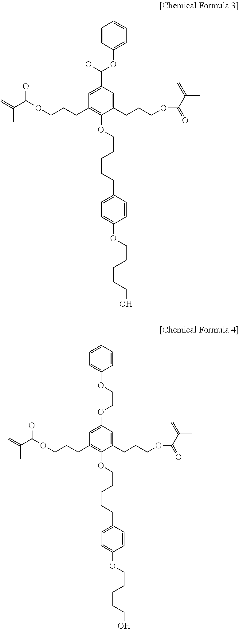
- the vertical alignment additive may be one or more of compounds represented by Chemical Formulas 1 to 5.
- a liquid crystal display including: a first substrate, a second substrate overlapping the first substrate and spaced apart therefrom, a liquid crystal layer between the first substrate and the second substrate and comprising liquid crystal molecules, a first alignment layer positioned between the first substrate and the liquid crystal layer; and a plurality of protrusions between the first alignment layer and the liquid crystal layer, wherein the first alignment layer comprises a photoinitiator, wherein the plurality of protrusions comprise a polymerization product of the photoinitiator, a reactive mesogen, and a vertical alignment additive, and wherein an alignment layer is not present between the second substrate and the liquid crystal layer.
- the vertical alignment additive may be less reactive than the photoinitiator.
- the vertical alignment additive may include a hydroxyl group at an end thereof.
- the vertical alignment additive does not include a biphenyl structure and may include two or more end groups represented by Chemical Formula 6, or the vertical alignment additive may include a biphenyl structure and may include two or more end groups represented by Chemical Formula 7.
- the liquid crystal display may have a curved shape.
- the photoinitiator may be benzophenone.
- No protrusion of the plurality of protrusions may be present between the second substrate and the liquid crystal layer.
- Liquid crystal molecules adjacent to the first substrate may be aligned at a pretilt angle, and liquid crystal molecules adjacent to the second substrate may be aligned at an angle perpendicular to the second substrate.
- a difference between the pretilt angle of the liquid crystal molecules adjacent to the first substrate and the angle of the liquid crystal molecules adjacent to the second substrate may be 0.2 degree or more.
- the vertical alignment additive may be one or more of compounds represented by Chemical Formulas 1 to 5.
- Yet another embodiment provides a method of manufacturing a liquid crystal display, including: providing a first substrate including a first alignment layer; providing a second substrate overlapping the first substrate; forming a liquid crystal layer including a plurality of liquid crystal molecules, a reactive mesogen, and a vertical alignment additive between the first substrate and the second substrate; irradiating ultraviolet (UV) light toward the first substrate and the second substrate, and polymerizing the photoinitiator, the reactive mesogen, and the vertical alignment additive to form the liquid crystal display, wherein the first alignment layer includes a photoinitiator, and wherein the photoinitiator, the reactive mesogen, and the vertical alignment additive may be polymerized by the ultraviolet light to form a plurality of protrusions on the first alignment layer.
- UV ultraviolet
- the photoinitiator may be benzophenone.
- the vertical alignment additive may be less reactive than the photoinitiator.
- a content of the vertical alignment additives may be about 0.1 weight percent (wt %) to about 3 wt % based on the total weight of the liquid crystal layer.
- liquid crystal molecules adjacent to the first substrate may be aligned at a pretilt angle
- liquid crystal molecules adjacent to the second substrate may be aligned at an angle perpendicular to the second substrate.
- a difference between the pretilt angle of the liquid crystal molecules adjacent to the first substrate and the angle of the liquid crystal molecules adjacent to the second substrate may be 0.2 degree or greater.
- the vertical alignment additive may include a hydroxyl group at an end thereof.
- the vertical alignment additive does not include a biphenyl structure and may include two or more end groups represented by Chemical Formula 6, or the vertical alignment additive may include a biphenyl structure and may include two or more end groups represented by Chemical Formula 7.
- the vertical alignment additive may be one or more of compounds represented by Chemical Formulas 1 to 5.
- a central wavelength of the UV light may be about 300 nanometers (nm) to about 350 nm.
- liquid crystal display and the manufacturing method thereof of the exemplary embodiment of the present invention it is possible to prevent texture occurrence.
- FIG. 1 is a schematic cross-sectional view of a liquid crystal display according to an exemplary embodiment of the present invention
- FIG. 2 is a schematic cross-sectional view of a liquid crystal display according to another exemplary embodiment of the present invention.
- FIG. 3 is a schematic illustration explaining the development of a texture defect caused by a misalignment which occurs when pretilt angles of liquid crystal molecules adjacent to upper and lower alignment layers are the same;
- FIG. 4 is a graph of absorbance (normalized, nor.) versus wavelength (nm) comparing the absorbance spectrums of a vertical alignment additive represented by Chemical Formula 1 and a benzophenone photoinitiator;
- FIG. 5 is a graph of absorbance (nor.) versus wavelength (nm) comparing the absorbance spectrums of a vertical alignment additive represented by Chemical Formula 2 and a benzophenone photoinitiator;
- FIG. 6 is a graph of absorbance (nor.) versus wavelength (nm) comparing the absorbance spectrums of a vertical alignment additive represented by Chemical Formula 3 and a benzophenone photoinitiator;
- FIG. 7 is a graph of absorbance (nor.) versus wavelength (nm) comparing the absorbance spectrums of a vertical alignment additive represented by Chemical Formula 4 and a benzophenone photoinitiator;
- FIG. 8 is a graph of absorbance (nor.) versus wavelength (nm) comparing the absorbance spectrums of a vertical alignment additive represented by Chemical Formula 5 and a benzophenone photoinitiator;
- FIG. 9 is a plan view of a single pixel of a liquid crystal display according to an exemplary embodiment.
- FIG. 10 is a cross-sectional view taken along line IX-IX of FIG. 9 ;
- FIG. 11 to FIG. 13 illustrate process cross-sectional views of a manufacturing method according to an exemplary embodiment of the present invention.
- “About” or “approximately” as used herein is inclusive of the stated value and means within an acceptable range of deviation for the particular value as determined by one of ordinary skill in the art, considering the measurement in question and the error associated with measurement of the particular quantity (i.e., the limitations of the measurement system). For example, “about” can mean within one or more standard deviations, or within ⁇ 30%, 20%, 10%, 5% of the stated value.
- the phrase “on a plane” means a view of the object or portion thereof from the top
- the phrase “on a cross-section” means a view of a cross-section of an object or a portion thereof which is vertically cut from the side.
- FIG. 1 illustrates a schematic cross-sectional view of a liquid crystal display according to an exemplary embodiment of the present invention.
- a liquid crystal display according to present exemplary embodiment includes a first substrate 110 , a second substrate 210 overlapping the first substrate 110 while being spaced apart from the first substrate 110 , a liquid crystal layer 3 positioned between the first substrate 110 and the second substrate 210 and including liquid crystal molecules 31 , a first alignment layer 11 positioned between the first substrate 110 and the liquid crystal layer 3 , and a plurality of protrusions 13 positioned between the first alignment layer 11 and the liquid crystal layer 3 .
- an alignment layer is not positioned (present) between the second substrate 210 and the liquid crystal layer 3 .
- pretilt means that a liquid crystal molecule 310 is tilted, or angled, relative to a direction perpendicular to a surface of the first alignment layer 11 or a second alignment layer 21
- pretilt angle means a degree to which the liquid crystal molecules is tilted, that is, a tilt angle based on an axis perpendicular to the first alignment layer 11 or the second alignment layer 21 .
- the first alignment layer 11 includes a photoinitiator
- the plurality of protrusions 13 are include a polymerization product of, that is, are formed of a polymer obtained by polymerizing a photoinitiator, a reactive mesogen, and a vertical alignment additive included in the first alignment layer 11 .
- the first alignment layer 11 which includes a photoinitiator, may contain benzophenone as the photoinitiator. The benzophenone serves to initiate the polymerization of the reactive mesogen and the vertical alignment additive.
- the first alignment layer 11 may include a compound represented by Chemical Formula 10 and a compound represented by Chemical Formula 11.
- the first alignment layer 11 may have a multi-layered structure, and in this case, a layer thereof which is closer to the first substrate 110 may include a compound represented by Chemical Formula 11, and a layer thereof which is closer to the liquid crystal layer 3 may include a compound represented by Chemical Formula 10.
- the compound represented by Chemical Formula 10 includes a benzophenone photoinitiator.
- the reactive mesogen may include one or more of an acrylate, a methacrylate, an epoxy, an oxetane, a vinyl-ether, or styrene.
- the vertical alignment additive of the present exemplary embodiment may include a hydroxyl group (OH) at an end thereof, preferably at one end thereof, but does not include a biphenyl structure, and may include two or more end groups represented by Chemical Formula 6.
- the vertical alignment additive may include a hydroxyl group (OH) at an end thereof, preferably at one end thereof, may have a biphenyl structure, and may include two or more end groups represented by Chemical Formula 7.
- the vertical alignment additive of the present exemplary embodiment may be one or more of groups formed by Chemical Formulas 1 to 5.
- the vertical alignment additive having the above-mentioned structure is less reactive than the photoinitiator included in the first alignment layer 11 . Accordingly, it is possible to prevent the vertical alignment additive from reacting with the reactive mesogen inside the liquid crystal layer to form a polymer.
- the reactive mesogen and the vertical alignment additive are mixed with the liquid crystal molecules and injected into the liquid crystal layer, and are then polymerized upon exposure to ultraviolet (UV) light irradiation to form the protrusions 13 .
- UV ultraviolet
- the vertical alignment additive contains a photoreactive group in the structure thereof. Without being limited by theory, it is understood that when the reactivity of the vertical alignment additive is higher than the reactivity of the photoinitiator included in the first alignment layer 11 , the vertical alignment additive does not react near the first alignment layer 11 but may instead react with the reactive mesogen or the like in the liquid crystal layer 3 and may thus be polymerized. When the vertical alignment additive is polymerized with the reactive mesogen in the liquid crystal layer, the polymerized polymer (polymerization product) may form the protrusions 13 at the second substrate 210 side.
- the protrusions 13 are not formed only in the first alignment layer 11 because the polymerization reaction occurs without the photoreactive group.
- the liquid crystal display according to the present exemplary embodiment uses a material having decreased reactivity than the photoinitiator included in the first alignment layer, as the vertical alignment additive. Accordingly, the vertical alignment additive does not react until all of the photoinitiator included in the first alignment layer has reacted. After all of the photoinitiator in the first alignment layer has reacted, the vertical alignment additive polymerizes with the reactive mesogen and the adjacent vertical alignment additive near to the first alignment layer to form the protrusions. Thus, the protrusions 13 are not formed on the second substrate 210 that does not include a photoinitiator or an alignment layer which induces the polymerization reaction.
- the photoinitiator included in the first alignment layer may be benzophenone.
- the reactivity of the vertical alignment additive represented by Chemical Formulas 1 to 5 is lower than the reactivity of the benzophenone.
- the first alignment layer 11 is formed only on the first substrate 110 , an alignment layer is not formed on the second substrate 210 , and a material having decreased reactivity than the photoinitiator included in the first alignment layer is used as the vertical alignment additive. Accordingly, the reaction of the vertical alignment additive occurs only the vicinity of the first alignment layer, i.e., the area in which the photoinitiator is positioned, and the vertical alignment additive is polymerized to form the protrusions 13 on the first alignment layer 11 , and the protrusions induce the pretilt in the liquid crystal molecules near to (e.g., adjacent to) the first alignment layer.
- the liquid crystal molecules near to the second substrate 210 in a UV light irradiation process are vertically aligned by the vertical alignment additive in the liquid crystal layer, but they are not tilted at a certain angle which is the same as the liquid crystal molecules near the first substrate 110 .
- the liquid crystal molecules 31 adjacent to the first substrate 110 are aligned so as to have a predetermined pretilt, and the liquid crystal molecules adjacent to the second substrate 210 are aligned in a direction perpendicular to the second substrate.
- a difference between the pretilt of the liquid crystal molecules adjacent to the first substrate 110 and the angle of the liquid crystal molecules adjacent to the second substrate 210 may be 0.2 degree or more.
- FIG. 2 is a cross-sectional view of a liquid crystal display according to an exemplary embodiment of the present invention.
- the liquid crystal display according to the present exemplary embodiment may be a curved liquid crystal display.
- the liquid crystal display of FIG. 2 has the same structure as that of FIG. 1 , except for having a curved structure, and a repeated description of the same structure will be omitted.
- FIG. 3 is a schematic view explaining the formation of a texture defect caused by a misalignment when pretilt angles of liquid crystal molecules adjacent to upper and lower alignment layers are the same.
- the pretilts are formed in both the liquid crystal molecules 31 adjacent to the first substrate 110 and the liquid crystal molecules 310 adjacent to the second substrate 210 , the first substrate 110 and the second substrate 210 are misaligned in a bending process.
- a misalignment region in which the pretilt direction of the liquid crystal molecules 310 adjacent to the first alignment layer 11 and the pretilt direction of the liquid crystal molecules 310 adjacent to the second alignment layer 21 , may occur.
- This misalignment region may be formed at a boundary of adjacent domains.
- a problem occurs in a direction in which the liquid crystal molecules 310 are tilted, and a texture defect occurs on a screen. Misalignment of the display panel may occur when the display panel is bent. The texture corresponds to a portion that appears darker than the surroundings and may be viewed as stains.
- the first alignment layer 11 and the protrusions 13 are only present on the first substrate 110 , the liquid crystal molecules near the first substrate 110 are aligned to have a tilt angle with respect to a vertical state (e.g., the pretilt angle), and since the second substrate 210 does not include an alignment layer or any protrusions, the liquid crystal molecules are aligned perpendicular to the substrate. Accordingly, when the first substrate 110 and the second substrate 210 are bent, it is difficult to prevent textures from occurring.
- a difference between the pretilt angle of the liquid crystal molecules adjacent to the first substrate 110 and the angle of the liquid crystal molecules adjacent to the second substrate 210 may be about 0.2 degree or greater. As can be seen from Table 1, this is an angle difference that may reduce an amount of luminance change before and after bending.
- Table 1 shows a change in transmittance and a luminance due to a pretilt difference between liquid crystal molecules of a lower substrate and liquid crystal molecules of an upper substrate of the liquid crystal display. That is, the luminance change amount in Table 1, is the difference between the luminance when the lower substrate and the upper substrate are aligned and when they are misaligned by 30 ⁇ m (i.e., in a case in which they are formed to have a curved shape).
- the pretilts of the liquid crystal molecules adjacent to the upper substrate are the same as the pretilts of the liquid crystal molecules adjacent to the lower substrate of the liquid crystal display, when the liquid crystal display is bent in a curved shape, the luminance change amount is as great as ⁇ 9%.
- the pretilt difference between the two substrates increases, the luminance change amount decreases, and when the pretilt angle difference is 1 degree, the luminance change amount is 0%. That is, when the pretilt angle difference between the two substrates was 1 degree, it was confirmed that the luminance did not decrease at all even when the liquid crystal display was misaligned to a level of 30 ⁇ m.
- the first alignment layer 11 and the protrusions 13 are positioned only on the first substrate 110 , and no alignment layer and no protrusions are positioned on the second substrate 210 , and the protrusions 13 are polymers obtained by polymerizing the photoinitiator, the reactive mesogen, and the vertical alignment additive included in the first alignment layer 11 .
- a material having decreased reactivity compared to the photoinitiator included in the first alignment layer 11 is used as a vertical alignment additive so that the protrusions 13 are formed only on the first substrate 110 .
- FIG. 4 to FIG. 8 are graphs comparing the absorbance spectrums of various vertical alignment additives and benzophenone photoinitiators.
- FIG. 4 is a graph comparing the absorbance spectrum of a vertical alignment additive represented by Chemical Formula 1 and a benzophenone photoinitiator
- FIG. 5 is a graph comparing the absorbance spectrums of a vertical alignment additive represented by Chemical Formula 2 and a benzophenone photoinitiator.
- FIG. 6 is a graph comparing the absorbance spectrums of a vertical alignment additive represented by Chemical Formula 3 and a benzophenone photoinitiator
- FIG. 7 is a graph comparing the absorbance spectrums of a vertical alignment additive represented by Chemical Formula 4 and a benzophenone photoinitiator.
- FIG. 8 is a graph comparing the absorbance spectrum of a vertical alignment additive represented by Chemical Formula 5 and a benzophenone photoinitiator.
- a central wavelength of the UV light used in the irradiation process is about 300 nm to about 350 nm, and the lower the absorbance spectrum for this wavelength range, the lower the reactivity.
- the compounds represented by Chemical Formula 1 to Chemical Formula 5 have a relatively lower absorbance spectra in comparison with benzophenone photoinitiators in the wavelength range of 300 nm to 350 nm.
- the vertical alignment additives corresponding to the compounds represented by Chemical Formula 1 to Chemical Formula 5 are less reactive than the benzophenone photoinitiator, and thus, when the vertical alignment additives are added to the liquid crystal layer and the UV light is irradiated thereto, the vertical alignment additives do not react earlier than the benzophenone photoinitiator. Accordingly, it is possible to prevent the formation of protrusions due to polymerization of the vertical alignment additives on the second substrate 210 in which the photoinitiator is not present.
- liquid crystal display according to the exemplary embodiment will be described more fully.
- this is merely an example, and the liquid crystal display of the present invention is not limited to the following structure.
- FIG. 9 is a plan view of a single pixel of a liquid crystal display according to an exemplary embodiment
- FIG. 10 illustrates a cross-sectional view of the pixel taken along line IX-IX of FIG. 9 .
- a first display panel 100 will be described first.
- a gate conductor including a gate line 121 and a divided reference voltage line 131 is positioned on the first substrate 110 made of transparent glass or plastic.
- the gate line 121 includes a first gate electrode 124 a , a second gate electrode 124 b , and a third gate electrode 124 c.
- the divided reference voltage line 131 includes first storage electrodes 135 and 136 , and a reference electrode 137 . Although not connected to the divided reference voltage line 131 , second storage electrodes 138 and 139 may be positioned to overlap a second subpixel electrode 191 b.
- a gate insulating layer 140 is positioned on the gate line 121 and the divided reference voltage line 131 .
- a first semiconductor layer 154 a , a second semiconductor layer 154 b , and a third semiconductor layer 154 c are positioned on the gate insulating layer 140 .
- Ohmic contact members 163 a , 165 a , 163 b , 165 b , 163 c , and 165 c are positioned on semiconductor layer 154 a , 154 b , and 154 c.
- the first gate electrode 124 a , the first source electrode 173 a , and the first drain electrode 175 a form a first thin film transistor along with the first semiconductor layer 154 a ;
- the second gate electrode 124 b , the second source electrode 173 b , and the second drain electrode 175 b form a second thin film transistor along with the second semiconductor layer 154 b ;
- the third gate electrode 124 c , the third source electrode 173 c , and the third drain electrode 175 c form a third thin film transistor along with the third semiconductor layer 154 c.
- the second drain electrode 175 b is connected to the third source electrode 173 c , and includes an extension portion 177 that is widely extended.
- a first passivation layer 180 p is positioned on the data conductors 171 , 173 c , 175 a , 175 b , and 175 c and on the semiconductor layers 154 a , 154 b , and 154 c.
- a color filter 230 is positioned on the first passivation layer 180 p .
- the color filter 230 extends in a vertical direction along two data lines 171 adjacent to each other.
- the color filter 230 is included in the first display panel 100 , but the present invention is not limited thereto, and the color filter 230 may be included in a second display panel 200 .
- a second passivation layer 180 q is positioned on the color filter 230 .
- the first passivation layer 180 p and the second passivation layer 180 q may include an inorganic insulating layer such as a silicon nitride or a silicon oxide.
- the second passivation layer 180 q prevents the color filter 230 from being lifted and suppresses contamination of the liquid crystal layer 3 by an organic material such as a solvent flowing from the color filters 230 , thereby preventing defects such as an afterimage while a screen is displayed.
- the first passivation layer 180 p and the second passivation layer 180 q are provided with a first contact hole 185 a and a second contact hole 185 b respectively overlapping the first drain electrode 175 a and the second drain electrode 175 b.
- the first passivation layer 180 p , the second passivation layer 180 q , and the gate insulating layer 140 are provided with a third contact hole 185 c overlapping some of the reference electrode 137 and some of the third drain electrode 175 c , and the third contact hole 185 c is covered by a connecting member 195 .
- the connecting member 195 electrically connects the reference electrode 137 overlapping the third contact hole 185 c and the third drain electrode 175 c.
- a pixel electrode 191 is positioned on the second passivation layer 180 q .
- the pixel electrode 191 corresponds to a field generating electrode, pixel electrodes 191 are separated from each other with the gate line 121 therebetween, and each of the pixel electrodes 191 includes a first subpixel electrode 191 a and the second subpixel electrode 191 b adjacent in a column direction based on the gate line 121 .
- the pixel electrode 191 may include a transparent material such as ITO and IZO.
- Each of the first subpixel electrode 191 a and the second subpixel electrode 191 b has a quadrangular shape, and includes a cross-shaped stem that is formed of a transverse stem 193 and a vertical stem 192 that is perpendicular thereto.
- each of the first subpixel electrode 191 a and the second subpixel electrode 191 b is divided into a first sub-region Da, a second sub-region Db, a third sub-region Dc, and a fourth sub-region Dd by the transverse stem 193 and the vertical stem 192 , and includes a plurality of minute branches 194 positioned in each of the sub-regions Da-Dd.
- the first subpixel electrode 191 a and the second subpixel electrode 191 b are respectively connected to the first drain electrode 175 a or the second drain electrode 175 b through the first contact hole 185 a and the second contact hole 185 b , thereby receiving a data voltage from the first drain electrode 175 a and the second drain electrode 175 b .
- some of the data voltage applied to the second drain electrode 175 b is divided by the third source electrode 173 c such that a voltage applied to the first subpixel electrode 191 a is greater than that applied to the second subpixel electrode 191 b.
- the first subpixel electrode 191 a and the second subpixel electrode 191 b to which a data voltage is applied, generate an electric field together with a common electrode 270 of the second display substrate 200 , thereby determining orientation of the liquid crystal molecules 31 of the liquid crystal layer 3 between the two electrodes 191 and 270 .
- Luminance of light passing through the liquid crystal layer 3 may vary depending on the determined orientation of the liquid crystal molecules 31 .
- the description related to the thin film transistor and the pixel electrode 191 described above is one example, and the structure of the thin film transistor and the design of the pixel electrode 191 may be varied to improve the lateral visibility.
- the first alignment layer 11 is positioned between the pixel electrode 191 and the liquid crystal layer 3 .
- a description of the first alignment layer 11 is the same as described in FIG. 1 and FIG. 2 .
- the first alignment layer may have a multi-layered structure, and in this case, a layer of the multi-layered structure adjacent to the first substrate 110 may include the compound represented by Chemical Formula 11, and a layer of the multi-layered structure adjacent to the liquid crystal layer 3 may include the compound represented by Chemical Formula 10.
- the first alignment layer 11 may include a photoinitiator, and in this case, the photoinitiator may be benzophenone.
- the protrusions 13 are positioned between the first alignment layer 11 and the liquid crystal layer 3 .
- the protrusions 13 are the same as the protrusions described with reference to FIG. 1 and FIG. 2 . That is, the protrusion 13 is formed of a polymerization product of, i.e., is formed of a polymer obtained by polymerizing, a photoinitiator, a reactive mesogen, and a vertical alignment additive. In this case, the vertical alignment additive is less reactive than the photoinitiator. A detailed description of the same constituent elements will be omitted.
- the second substrate 210 is positioned to overlap the first substrate 110 while being spaced apart from the first substrate 110 .
- a light blocking member 220 is positioned between the second substrate 210 and the liquid crystal layer 3 .
- the light blocking member 220 is positioned so as to overlap a region in which the data line 171 of the first display panel 100 is positioned and a region in which the thin film transistor, and the like, are positioned.
- the light blocking member 220 is included in the second display panel 200 , the present invention is not limited thereto, and the light blocking member may be included in the first display panel 100 .
- An overcoat 250 is positioned between the light blocking member 220 and the liquid crystal layer 3 .
- the overcoat 250 may be omitted.
- the common electrode 270 is positioned between the overcoat 250 and the liquid crystal layer 3 .
- the common electrode 270 generates an electric field together with the pixel electrode 191 of the first display panel 100 , thereby determining orientation of the liquid crystal molecules 31 of the liquid crystal layer 3 .
- No alignment layer and protrusion are provided at the second substrate 210 .
- the liquid crystal layer 3 includes the liquid crystal molecules 31 .
- the liquid crystal layer 3 may include some of an unreacted vertical alignment additive and a reactive mesogen.
- the vertical alignment additive and the reactive mesogen are included inside the liquid crystal layer and then react by a UV light irradiation process to form protrusions, and in this case, some of the vertical alignment additive and the reactive mesogen may remain in the liquid crystal layer.
- FIG. 11 , FIG. 12 , and FIG. 13 are cross-sectional views illustrating a method of manufacturing according liquid crystal display to an exemplary embodiment of the present invention.
- the first substrate 110 provided with the first alignment layer 11 and the second substrate 210 overlapping the first substrate 110 are provided (e.g., prepared).
- the first alignment layer 11 is positioned only on the first substrate 110 , and is not positioned on the second substrate 210 .
- a thin film transistor and a pixel electrode may be positioned at the first substrate 110
- a common electrode may be positioned at the second substrate 210 .
- both a pixel electrode and a common electrode may be positioned at the first substrate 110 .
- the first alignment layer 11 may include a photoinitiator, and the photoinitiator may be benzophenone.
- the first alignment layer 11 may include a compound represented by Chemical Formula 10.
- the liquid crystal layer 3 including a plurality of liquid crystal molecules 31 , a reactive mesogen 15 , and a vertical alignment additive 25 is formed between the first substrate 110 and the second substrate 210 , which overlap each other.
- the reactive mesogen 15 may be one or more of an acrylate, a methacrylate, an epoxy, an oxetane, a vinyl-ether, or a styrene.
- the vertical alignment additive 25 includes a material that is less reactive than the photoinitiator of the first alignment layer 11 . Specifically, with respect to ultraviolet light having a central wavelength of about 300 nm to about 350 nm, the absorbance of the vertical alignment additive is lower than the absorbance of the photoinitiator.
- the vertical alignment additive 25 may include a hydroxyl group at an end thereof, preferably at one end thereof, does not include a biphenyl structure, and may include two or more end groups represented by Chemical Formula 6.
- the vertical alignment additive 25 may include a hydroxyl group at an end thereof, preferably at one end thereof, may include a biphenyl structure, and may include two or more end groups represented by Chemical Formula 7.
- the vertical alignment additive 25 may be one or more of compounds represented by Chemical Formulas 1 to 5.
- a content of the vertical alignment additive 25 may be 0.1 wt % to 3 wt % with respect to the total weight of the liquid crystal layer 3 .
- the content is less than 0.1 wt %, the liquid crystal molecules 31 may not be sufficiently vertically aligned, and when the content is greater than 3 wt %, the vertical alignment additive 25 may not be dissolved in the liquid crystal layer 3 .
- UV light is irradiated toward the first substrate 110 and the second substrate 210 .
- a central wavelength of the irradiated UV light may be about 300 nm to about 350 nm.
- the photoinitiator included in the first alignment layer is activated by the irradiation of the UV light, and the reactive mesogen 15 and the vertical alignment additive 25 react with each other in the vicinity of the photoinitiator and are polymerized. Unreacted vertical alignment additive 25 remains inside of the liquid crystal layer, and vertically aligns the liquid crystal molecules 31 .
- the protrusions 13 are formed by the polymerization process which occurs on the first alignment layer 11 as a result the UV light irradiation of the previous process.
- the protrusions 13 are thus formed of a polymer obtained by polymerizing the photoinitiator, the reactive mesogen 15 , and the vertical alignment additive 25 .
- the liquid crystal molecules adjacent to the first substrate 110 Due to the formation of the protrusions 13 , the liquid crystal molecules adjacent to the first substrate 110 have a pretilt. However, the second substrate 210 is not provided with an alignment layer, thus no protrusion 13 is formed at the second substrate because there is no photoinitiator present to induce the polymerization reaction between the reactive mesogen 15 and the vertical alignment additive 25 . Accordingly, the liquid crystal molecules adjacent to the second substrate 210 are aligned to be perpendicular to the second substrate 210 .
- the pretilt angle of the liquid crystal molecules 31 adjacent to the first substrate 110 is different from the angle of the liquid crystal molecules 31 adjacent to the second substrate 210 , and as a result the texture defects may be prevented from occurring when the liquid crystal display is bent in a curved shape.
- the pretilt angle difference occurs because the first alignment layer 11 and the protrusions 13 are positioned only on the first substrate 110 .
- the reason that the protrusions 13 are formed only on the first alignment layer 11 is because the reaction between the vertical alignment additives 25 or between the vertical alignment additive 25 and the reactive mesogen 15 is blocked in the absence of the photoinitiator by using the vertical alignment additive 25 made of a less reactive material than the photoinitiator.
Landscapes
- Physics & Mathematics (AREA)
- Chemical & Material Sciences (AREA)
- Nonlinear Science (AREA)
- Crystallography & Structural Chemistry (AREA)
- General Physics & Mathematics (AREA)
- Mathematical Physics (AREA)
- Optics & Photonics (AREA)
- Spectroscopy & Molecular Physics (AREA)
- Organic Chemistry (AREA)
- Chemical Kinetics & Catalysis (AREA)
- Materials Engineering (AREA)
- Engineering & Computer Science (AREA)
- Wood Science & Technology (AREA)
- Life Sciences & Earth Sciences (AREA)
- Health & Medical Sciences (AREA)
- Medicinal Chemistry (AREA)
- Polymers & Plastics (AREA)
- Liquid Crystal (AREA)
Abstract
Description


| TABLE 1 | ||
| Pretilt (degree) | Transmittance simulation | Luminance |
| Lower | Upper | Differ- | (a.u.) | change |
| substrate | substrate | ence | Alignment | 30 um M/A | amount |
| 89.0 | 90.0 | 1.0 | 0.17072 | 0.17072 | 0.0 % |
| 89.8 | 0.8 | 0.17191 | 0.16988 | −1.2 % | |
| 89.5 | 0.5 | 0.17339 | 0.16651 | −4.0 % | |
| 89.2 | 0.2 | 0.17459 | 0.1625 | −6.9 % | |
| 89.0 | 0.0 | 0.17527 | 0.15955 | −9.0 % | |


Claims (20)


Applications Claiming Priority (2)
| Application Number | Priority Date | Filing Date | Title |
|---|---|---|---|
| KR1020170106151A KR102456697B1 (en) | 2017-08-22 | 2017-08-22 | Liquid crystal display and manufacturing method thereof |
| KR10-2017-0106151 | 2017-08-22 |
Publications (2)
| Publication Number | Publication Date |
|---|---|
| US20190064605A1 US20190064605A1 (en) | 2019-02-28 |
| US11391992B2 true US11391992B2 (en) | 2022-07-19 |
Family
ID=63077786
Family Applications (1)
| Application Number | Title | Priority Date | Filing Date |
|---|---|---|---|
| US15/981,032 Active 2038-10-30 US11391992B2 (en) | 2017-08-22 | 2018-05-16 | Liquid crystal display and manufacturing method thereof |
Country Status (4)
| Country | Link |
|---|---|
| US (1) | US11391992B2 (en) |
| EP (1) | EP3447573A1 (en) |
| KR (1) | KR102456697B1 (en) |
| CN (1) | CN109426037B (en) |
Families Citing this family (5)
| Publication number | Priority date | Publication date | Assignee | Title |
|---|---|---|---|---|
| CN109828403B (en) * | 2019-03-08 | 2021-08-20 | 华南师范大学 | A kind of electric response reflection device and preparation method thereof |
| CN111025775A (en) * | 2019-12-16 | 2020-04-17 | 深圳市华星光电半导体显示技术有限公司 | Curved surface screen |
| CN111240100B (en) * | 2020-03-06 | 2021-07-06 | Tcl华星光电技术有限公司 | A flexible liquid crystal display panel and its preparation method |
| CN113325633B (en) * | 2021-05-17 | 2023-10-17 | Tcl华星光电技术有限公司 | Display panel and preparation method thereof |
| CN113406826B (en) | 2021-06-16 | 2022-09-27 | 惠州华星光电显示有限公司 | Liquid crystal display panel, preparation method of liquid crystal display panel and curved-surface type display |
Citations (17)
| Publication number | Priority date | Publication date | Assignee | Title |
|---|---|---|---|---|
| US20050116200A1 (en) | 2002-04-16 | 2005-06-02 | Fujitsu Display Technologies Corporation | Liquid crystal display device |
| EP1340118B1 (en) | 2000-11-23 | 2011-02-16 | Merck Patent GmbH | Homeotropic alignment layer |
| US20110102720A1 (en) * | 2008-06-27 | 2011-05-05 | Masanobu Mizusaki | Liquid crystal display device and manufacturing method therefor |
| WO2012038026A1 (en) | 2010-09-25 | 2012-03-29 | Merck Patent Gmbh | Liquid crystal displays and liquid crystalline media with homeotropic alignment |
| US20140240649A1 (en) * | 2013-02-26 | 2014-08-28 | Innolux Corporation | Display device |
| WO2014142168A1 (en) * | 2013-03-12 | 2014-09-18 | 日産化学工業株式会社 | Liquid crystal aligning agent containing crosslinkable compound having photoreactive group |
| JP2014218664A (en) | 2013-05-03 | 2014-11-20 | 三星ディスプレイ株式會社Samsung Display Co.,Ltd. | Liquid crystal composition, liquid crystal display device, and production method of liquid crystal display device |
| US20150085236A1 (en) * | 2012-03-05 | 2015-03-26 | Sharp Kabushiki Kaisha | Liquid crystal display device and method for manufacturing liquid crystal display device |
| US20150378193A1 (en) * | 2014-06-30 | 2015-12-31 | Samsung Display Co., Ltd. | Curved display device and method of manufacturing the same |
| KR20160002599A (en) | 2014-06-30 | 2016-01-08 | 삼성디스플레이 주식회사 | Curved display device and method for manufacturing the same |
| US20160026041A1 (en) | 2014-07-25 | 2016-01-28 | Samsung Display Co., Ltd. | Fabrication method of display device and display device |
| KR101618785B1 (en) | 2014-09-29 | 2016-05-09 | 명지대학교 산학협력단 | Liquid crystal alignment layer, vertical alignment liquid crystal device using the same and method for manufacturing the same |
| US20160170268A1 (en) * | 2014-12-10 | 2016-06-16 | Samsung Display Co., Ltd. | Curved liquid crystal display |
| CN105733608A (en) * | 2016-04-22 | 2016-07-06 | 深圳市华星光电技术有限公司 | Liquid crystal material, making method of liquid crystal display panel and liquid crystal display panel |
| US20160274389A1 (en) | 2015-03-16 | 2016-09-22 | Samsung Display Co., Ltd. | Liquid crystal display and manufacturing method thereof |
| KR20170010242A (en) | 2015-07-17 | 2017-01-26 | 삼성디스플레이 주식회사 | Liquid crystal display |
| US20170059941A1 (en) | 2015-08-25 | 2017-03-02 | Samsung Display Co. Ltd. | Curved liquid crystal display and method of manufacturing the same |
Family Cites Families (8)
| Publication number | Priority date | Publication date | Assignee | Title |
|---|---|---|---|---|
| JP3714796B2 (en) * | 1998-05-29 | 2005-11-09 | シャープ株式会社 | Liquid crystal display device |
| US7777847B2 (en) * | 2004-06-11 | 2010-08-17 | Dai Nippon Printing Co., Ltd. | Liquid crystal display and manufacturing method of the same |
| KR101665529B1 (en) * | 2010-04-21 | 2016-10-13 | 삼성디스플레이 주식회사 | Liquid crystal display device and manufacturing method thereof |
| CN103064208B (en) * | 2013-01-23 | 2015-06-10 | 深圳市华星光电技术有限公司 | Polymer stable vertical alignment liquid crystal display panel and liquid crystal display |
| US9659965B2 (en) * | 2014-09-12 | 2017-05-23 | Samsung Display Co., Ltd. | Liquid crystal display device and method of manufacturing the same |
| KR20160090451A (en) * | 2015-01-21 | 2016-08-01 | 삼성디스플레이 주식회사 | Liquid crystal display and manufacturing method thereof |
| KR102323244B1 (en) * | 2015-04-29 | 2021-11-08 | 삼성디스플레이 주식회사 | Liquid crystal display and method of manufacturing the same |
| EP3162875B1 (en) * | 2015-10-30 | 2018-05-23 | Merck Patent GmbH | Polymerisable compounds and the use thereof in liquid-crystal displays |
-
2017
- 2017-08-22 KR KR1020170106151A patent/KR102456697B1/en active Active
-
2018
- 2018-05-16 US US15/981,032 patent/US11391992B2/en active Active
- 2018-07-26 EP EP18185810.1A patent/EP3447573A1/en not_active Withdrawn
- 2018-08-22 CN CN201810959261.4A patent/CN109426037B/en active Active
Patent Citations (21)
| Publication number | Priority date | Publication date | Assignee | Title |
|---|---|---|---|---|
| EP1340118B1 (en) | 2000-11-23 | 2011-02-16 | Merck Patent GmbH | Homeotropic alignment layer |
| US20050116200A1 (en) | 2002-04-16 | 2005-06-02 | Fujitsu Display Technologies Corporation | Liquid crystal display device |
| US7169449B2 (en) | 2002-04-16 | 2007-01-30 | Sharp Kabushiki Kaisha | Liquid crystal display device |
| US20110102720A1 (en) * | 2008-06-27 | 2011-05-05 | Masanobu Mizusaki | Liquid crystal display device and manufacturing method therefor |
| WO2012038026A1 (en) | 2010-09-25 | 2012-03-29 | Merck Patent Gmbh | Liquid crystal displays and liquid crystalline media with homeotropic alignment |
| US20130182202A1 (en) | 2010-09-25 | 2013-07-18 | Merck Patent Gesellschaft Mit Beschrankter Haftung | Liquid crystal displays and liquid crystalline media with homeotropic alignment |
| US20150085236A1 (en) * | 2012-03-05 | 2015-03-26 | Sharp Kabushiki Kaisha | Liquid crystal display device and method for manufacturing liquid crystal display device |
| US20140240649A1 (en) * | 2013-02-26 | 2014-08-28 | Innolux Corporation | Display device |
| WO2014142168A1 (en) * | 2013-03-12 | 2014-09-18 | 日産化学工業株式会社 | Liquid crystal aligning agent containing crosslinkable compound having photoreactive group |
| JP2014218664A (en) | 2013-05-03 | 2014-11-20 | 三星ディスプレイ株式會社Samsung Display Co.,Ltd. | Liquid crystal composition, liquid crystal display device, and production method of liquid crystal display device |
| US20150378193A1 (en) * | 2014-06-30 | 2015-12-31 | Samsung Display Co., Ltd. | Curved display device and method of manufacturing the same |
| KR20160002599A (en) | 2014-06-30 | 2016-01-08 | 삼성디스플레이 주식회사 | Curved display device and method for manufacturing the same |
| US20160026041A1 (en) | 2014-07-25 | 2016-01-28 | Samsung Display Co., Ltd. | Fabrication method of display device and display device |
| KR101618785B1 (en) | 2014-09-29 | 2016-05-09 | 명지대학교 산학협력단 | Liquid crystal alignment layer, vertical alignment liquid crystal device using the same and method for manufacturing the same |
| US20160170268A1 (en) * | 2014-12-10 | 2016-06-16 | Samsung Display Co., Ltd. | Curved liquid crystal display |
| US20160274389A1 (en) | 2015-03-16 | 2016-09-22 | Samsung Display Co., Ltd. | Liquid crystal display and manufacturing method thereof |
| KR20170010242A (en) | 2015-07-17 | 2017-01-26 | 삼성디스플레이 주식회사 | Liquid crystal display |
| US20170059941A1 (en) | 2015-08-25 | 2017-03-02 | Samsung Display Co. Ltd. | Curved liquid crystal display and method of manufacturing the same |
| KR20170024630A (en) | 2015-08-25 | 2017-03-08 | 삼성디스플레이 주식회사 | Curved liquid crystal display and method of manufacturing the same |
| CN105733608A (en) * | 2016-04-22 | 2016-07-06 | 深圳市华星光电技术有限公司 | Liquid crystal material, making method of liquid crystal display panel and liquid crystal display panel |
| US20180120652A1 (en) * | 2016-04-22 | 2018-05-03 | Shenzhen China Star Optoelectronics Technology Co., Ltd. | Liquid crystal materials, methods of fabricating liquid crystal display panels and liquid crystal display panels |
Non-Patent Citations (2)
| Title |
|---|
| Extended European Search Report dated Nov. 6, 2018, of the corresponding European Patent Application No. 18185810.1. |
| Office Action dated Oct. 7, 2021 of the corresponding Korean Patent Application No. 10-2017-0106151. |
Also Published As
| Publication number | Publication date |
|---|---|
| KR20190021517A (en) | 2019-03-06 |
| EP3447573A1 (en) | 2019-02-27 |
| US20190064605A1 (en) | 2019-02-28 |
| KR102456697B1 (en) | 2022-10-19 |
| CN109426037A (en) | 2019-03-05 |
| CN109426037B (en) | 2023-03-07 |
Similar Documents
| Publication | Publication Date | Title |
|---|---|---|
| US11391992B2 (en) | Liquid crystal display and manufacturing method thereof | |
| JP6348360B2 (en) | Liquid crystal display device and manufacturing method thereof | |
| CN102236210B (en) | Liquid crystal display and manufacture method thereof | |
| US10018875B2 (en) | Curved liquid crystal display and method of manufacturing the same | |
| US20110141416A1 (en) | Liquid crystal display and manufacturing method thereof | |
| US10558087B2 (en) | Liquid crystal display and manufacturing method thereof | |
| US9360709B2 (en) | Liquid crystal display device | |
| US10527890B2 (en) | Liquid crystal display and manufacturing method thereof | |
| US10088709B2 (en) | Alignment layer composition, liquid crystal display including the same, and method of manufacturing the liquid crystal display | |
| US20160209707A1 (en) | Liquid crystal display and manufacturing method of making the liquid crystal display | |
| US9823514B2 (en) | Liquid crystal display and method for manufacturing the same | |
| US9977288B2 (en) | Liquid crystal display | |
| US9567527B2 (en) | Alignment layer and liquid crystal display including the same | |
| US20170031213A1 (en) | Liquid crystal display | |
| US20150198846A1 (en) | Liquid crystal display | |
| US10503017B2 (en) | Liquid crystal display and manufacturing method thereof | |
| US10002890B2 (en) | Liquid crystal display | |
| US9658496B2 (en) | Manufacturing method of liquid crystal display | |
| US9671648B2 (en) | Liquid crystal display and method of manufacturing the same | |
| US20150253628A1 (en) | Liquid crystal display device, method of manufacturing the same, and alignment layer composition | |
| US10133123B2 (en) | Liquid crystal photo alignment agent and method of manufacturing liquid crystal display using the same | |
| US10620480B2 (en) | Liquid crystal display | |
| US9746714B2 (en) | Display device and method of manufacturing the same | |
| US11156874B2 (en) | Liquid crystal photoalignment agent and liquid crystal display including the same | |
| US9315668B2 (en) | Liquid crystal display |
Legal Events
| Date | Code | Title | Description |
|---|---|---|---|
| FEPP | Fee payment procedure |
Free format text: ENTITY STATUS SET TO UNDISCOUNTED (ORIGINAL EVENT CODE: BIG.); ENTITY STATUS OF PATENT OWNER: LARGE ENTITY |
|
| STPP | Information on status: patent application and granting procedure in general |
Free format text: DOCKETED NEW CASE - READY FOR EXAMINATION |
|
| STPP | Information on status: patent application and granting procedure in general |
Free format text: NON FINAL ACTION MAILED |
|
| STPP | Information on status: patent application and granting procedure in general |
Free format text: RESPONSE TO NON-FINAL OFFICE ACTION ENTERED AND FORWARDED TO EXAMINER |
|
| STPP | Information on status: patent application and granting procedure in general |
Free format text: ADVISORY ACTION MAILED |
|
| STPP | Information on status: patent application and granting procedure in general |
Free format text: DOCKETED NEW CASE - READY FOR EXAMINATION |
|
| STPP | Information on status: patent application and granting procedure in general |
Free format text: NON FINAL ACTION MAILED |
|
| STPP | Information on status: patent application and granting procedure in general |
Free format text: RESPONSE TO NON-FINAL OFFICE ACTION ENTERED AND FORWARDED TO EXAMINER |
|
| STPP | Information on status: patent application and granting procedure in general |
Free format text: FINAL REJECTION MAILED |
|
| STPP | Information on status: patent application and granting procedure in general |
Free format text: RESPONSE AFTER FINAL ACTION FORWARDED TO EXAMINER |
|
| STPP | Information on status: patent application and granting procedure in general |
Free format text: ADVISORY ACTION MAILED |
|
| STPP | Information on status: patent application and granting procedure in general |
Free format text: DOCKETED NEW CASE - READY FOR EXAMINATION |
|
| STPP | Information on status: patent application and granting procedure in general |
Free format text: NON FINAL ACTION MAILED |
|
| STPP | Information on status: patent application and granting procedure in general |
Free format text: RESPONSE TO NON-FINAL OFFICE ACTION ENTERED AND FORWARDED TO EXAMINER |
|
| STPP | Information on status: patent application and granting procedure in general |
Free format text: NOTICE OF ALLOWANCE MAILED -- APPLICATION RECEIVED IN OFFICE OF PUBLICATIONS |
|
| AS | Assignment |
Owner name: SAMSUNG DISPLAY CO., LTD., KOREA, REPUBLIC OF Free format text: ASSIGNMENT OF ASSIGNORS INTEREST;ASSIGNORS:KWON, OH JEONG;KIM, KA EUN;KIM, TAE MIN;AND OTHERS;REEL/FRAME:059335/0711 Effective date: 20171228 |
|
| STPP | Information on status: patent application and granting procedure in general |
Free format text: PUBLICATIONS -- ISSUE FEE PAYMENT VERIFIED |
|
| STCF | Information on status: patent grant |
Free format text: PATENTED CASE |
|
| MAFP | Maintenance fee payment |
Free format text: PAYMENT OF MAINTENANCE FEE, 4TH YEAR, LARGE ENTITY (ORIGINAL EVENT CODE: M1551); ENTITY STATUS OF PATENT OWNER: LARGE ENTITY Year of fee payment: 4 |