US11385740B2 - Organic light-emitting display panel and method for driving the same, and display device - Google Patents
Organic light-emitting display panel and method for driving the same, and display device Download PDFInfo
- Publication number
- US11385740B2 US11385740B2 US17/213,000 US202117213000A US11385740B2 US 11385740 B2 US11385740 B2 US 11385740B2 US 202117213000 A US202117213000 A US 202117213000A US 11385740 B2 US11385740 B2 US 11385740B2
- Authority
- US
- United States
- Prior art keywords
- rows
- emitting
- light
- driving circuit
- pixels
- Prior art date
- Legal status (The legal status is an assumption and is not a legal conclusion. Google has not performed a legal analysis and makes no representation as to the accuracy of the status listed.)
- Active
Links
Images


Classifications
-
- G—PHYSICS
- G09—EDUCATION; CRYPTOGRAPHY; DISPLAY; ADVERTISING; SEALS
- G09G—ARRANGEMENTS OR CIRCUITS FOR CONTROL OF INDICATING DEVICES USING STATIC MEANS TO PRESENT VARIABLE INFORMATION
- G09G3/00—Control arrangements or circuits, of interest only in connection with visual indicators other than cathode-ray tubes
- G09G3/20—Control arrangements or circuits, of interest only in connection with visual indicators other than cathode-ray tubes for presentation of an assembly of a number of characters, e.g. a page, by composing the assembly by combination of individual elements arranged in a matrix no fixed position being assigned to or needed to be assigned to the individual characters or partial characters
- G09G3/22—Control arrangements or circuits, of interest only in connection with visual indicators other than cathode-ray tubes for presentation of an assembly of a number of characters, e.g. a page, by composing the assembly by combination of individual elements arranged in a matrix no fixed position being assigned to or needed to be assigned to the individual characters or partial characters using controlled light sources
- G09G3/30—Control arrangements or circuits, of interest only in connection with visual indicators other than cathode-ray tubes for presentation of an assembly of a number of characters, e.g. a page, by composing the assembly by combination of individual elements arranged in a matrix no fixed position being assigned to or needed to be assigned to the individual characters or partial characters using controlled light sources using electroluminescent panels
- G09G3/32—Control arrangements or circuits, of interest only in connection with visual indicators other than cathode-ray tubes for presentation of an assembly of a number of characters, e.g. a page, by composing the assembly by combination of individual elements arranged in a matrix no fixed position being assigned to or needed to be assigned to the individual characters or partial characters using controlled light sources using electroluminescent panels semiconductive, e.g. using light-emitting diodes [LED]
- G09G3/3208—Control arrangements or circuits, of interest only in connection with visual indicators other than cathode-ray tubes for presentation of an assembly of a number of characters, e.g. a page, by composing the assembly by combination of individual elements arranged in a matrix no fixed position being assigned to or needed to be assigned to the individual characters or partial characters using controlled light sources using electroluminescent panels semiconductive, e.g. using light-emitting diodes [LED] organic, e.g. using organic light-emitting diodes [OLED]
-
- G—PHYSICS
- G06—COMPUTING OR CALCULATING; COUNTING
- G06F—ELECTRIC DIGITAL DATA PROCESSING
- G06F3/00—Input arrangements for transferring data to be processed into a form capable of being handled by the computer; Output arrangements for transferring data from processing unit to output unit, e.g. interface arrangements
- G06F3/01—Input arrangements or combined input and output arrangements for interaction between user and computer
- G06F3/03—Arrangements for converting the position or the displacement of a member into a coded form
- G06F3/041—Digitisers, e.g. for touch screens or touch pads, characterised by the transducing means
- G06F3/0416—Control or interface arrangements specially adapted for digitisers
- G06F3/04166—Details of scanning methods, e.g. sampling time, grouping of sub areas or time sharing with display driving
-
- G—PHYSICS
- G06—COMPUTING OR CALCULATING; COUNTING
- G06F—ELECTRIC DIGITAL DATA PROCESSING
- G06F3/00—Input arrangements for transferring data to be processed into a form capable of being handled by the computer; Output arrangements for transferring data from processing unit to output unit, e.g. interface arrangements
- G06F3/01—Input arrangements or combined input and output arrangements for interaction between user and computer
- G06F3/03—Arrangements for converting the position or the displacement of a member into a coded form
- G06F3/041—Digitisers, e.g. for touch screens or touch pads, characterised by the transducing means
- G06F3/0412—Digitisers structurally integrated in a display
-
- G—PHYSICS
- G06—COMPUTING OR CALCULATING; COUNTING
- G06F—ELECTRIC DIGITAL DATA PROCESSING
- G06F3/00—Input arrangements for transferring data to be processed into a form capable of being handled by the computer; Output arrangements for transferring data from processing unit to output unit, e.g. interface arrangements
- G06F3/01—Input arrangements or combined input and output arrangements for interaction between user and computer
- G06F3/03—Arrangements for converting the position or the displacement of a member into a coded form
- G06F3/041—Digitisers, e.g. for touch screens or touch pads, characterised by the transducing means
- G06F3/0416—Control or interface arrangements specially adapted for digitisers
- G06F3/0418—Control or interface arrangements specially adapted for digitisers for error correction or compensation, e.g. based on parallax, calibration or alignment
- G06F3/04184—Synchronisation with the driving of the display or the backlighting unit to avoid interferences generated internally
-
- G—PHYSICS
- G09—EDUCATION; CRYPTOGRAPHY; DISPLAY; ADVERTISING; SEALS
- G09G—ARRANGEMENTS OR CIRCUITS FOR CONTROL OF INDICATING DEVICES USING STATIC MEANS TO PRESENT VARIABLE INFORMATION
- G09G3/00—Control arrangements or circuits, of interest only in connection with visual indicators other than cathode-ray tubes
- G09G3/20—Control arrangements or circuits, of interest only in connection with visual indicators other than cathode-ray tubes for presentation of an assembly of a number of characters, e.g. a page, by composing the assembly by combination of individual elements arranged in a matrix no fixed position being assigned to or needed to be assigned to the individual characters or partial characters
- G09G3/22—Control arrangements or circuits, of interest only in connection with visual indicators other than cathode-ray tubes for presentation of an assembly of a number of characters, e.g. a page, by composing the assembly by combination of individual elements arranged in a matrix no fixed position being assigned to or needed to be assigned to the individual characters or partial characters using controlled light sources
- G09G3/30—Control arrangements or circuits, of interest only in connection with visual indicators other than cathode-ray tubes for presentation of an assembly of a number of characters, e.g. a page, by composing the assembly by combination of individual elements arranged in a matrix no fixed position being assigned to or needed to be assigned to the individual characters or partial characters using controlled light sources using electroluminescent panels
- G09G3/32—Control arrangements or circuits, of interest only in connection with visual indicators other than cathode-ray tubes for presentation of an assembly of a number of characters, e.g. a page, by composing the assembly by combination of individual elements arranged in a matrix no fixed position being assigned to or needed to be assigned to the individual characters or partial characters using controlled light sources using electroluminescent panels semiconductive, e.g. using light-emitting diodes [LED]
- G09G3/3208—Control arrangements or circuits, of interest only in connection with visual indicators other than cathode-ray tubes for presentation of an assembly of a number of characters, e.g. a page, by composing the assembly by combination of individual elements arranged in a matrix no fixed position being assigned to or needed to be assigned to the individual characters or partial characters using controlled light sources using electroluminescent panels semiconductive, e.g. using light-emitting diodes [LED] organic, e.g. using organic light-emitting diodes [OLED]
- G09G3/3266—Details of drivers for scan electrodes
-
- G—PHYSICS
- G09—EDUCATION; CRYPTOGRAPHY; DISPLAY; ADVERTISING; SEALS
- G09G—ARRANGEMENTS OR CIRCUITS FOR CONTROL OF INDICATING DEVICES USING STATIC MEANS TO PRESENT VARIABLE INFORMATION
- G09G3/00—Control arrangements or circuits, of interest only in connection with visual indicators other than cathode-ray tubes
- G09G3/20—Control arrangements or circuits, of interest only in connection with visual indicators other than cathode-ray tubes for presentation of an assembly of a number of characters, e.g. a page, by composing the assembly by combination of individual elements arranged in a matrix no fixed position being assigned to or needed to be assigned to the individual characters or partial characters
- G09G3/22—Control arrangements or circuits, of interest only in connection with visual indicators other than cathode-ray tubes for presentation of an assembly of a number of characters, e.g. a page, by composing the assembly by combination of individual elements arranged in a matrix no fixed position being assigned to or needed to be assigned to the individual characters or partial characters using controlled light sources
- G09G3/30—Control arrangements or circuits, of interest only in connection with visual indicators other than cathode-ray tubes for presentation of an assembly of a number of characters, e.g. a page, by composing the assembly by combination of individual elements arranged in a matrix no fixed position being assigned to or needed to be assigned to the individual characters or partial characters using controlled light sources using electroluminescent panels
- G09G3/32—Control arrangements or circuits, of interest only in connection with visual indicators other than cathode-ray tubes for presentation of an assembly of a number of characters, e.g. a page, by composing the assembly by combination of individual elements arranged in a matrix no fixed position being assigned to or needed to be assigned to the individual characters or partial characters using controlled light sources using electroluminescent panels semiconductive, e.g. using light-emitting diodes [LED]
- G09G3/3208—Control arrangements or circuits, of interest only in connection with visual indicators other than cathode-ray tubes for presentation of an assembly of a number of characters, e.g. a page, by composing the assembly by combination of individual elements arranged in a matrix no fixed position being assigned to or needed to be assigned to the individual characters or partial characters using controlled light sources using electroluminescent panels semiconductive, e.g. using light-emitting diodes [LED] organic, e.g. using organic light-emitting diodes [OLED]
- G09G3/3275—Details of drivers for data electrodes
-
- G—PHYSICS
- G09—EDUCATION; CRYPTOGRAPHY; DISPLAY; ADVERTISING; SEALS
- G09G—ARRANGEMENTS OR CIRCUITS FOR CONTROL OF INDICATING DEVICES USING STATIC MEANS TO PRESENT VARIABLE INFORMATION
- G09G2300/00—Aspects of the constitution of display devices
- G09G2300/08—Active matrix structure, i.e. with use of active elements, inclusive of non-linear two terminal elements, in the pixels together with light emitting or modulating elements
- G09G2300/0809—Several active elements per pixel in active matrix panels
- G09G2300/0842—Several active elements per pixel in active matrix panels forming a memory circuit, e.g. a dynamic memory with one capacitor
- G09G2300/0861—Several active elements per pixel in active matrix panels forming a memory circuit, e.g. a dynamic memory with one capacitor with additional control of the display period without amending the charge stored in a pixel memory, e.g. by means of additional select electrodes
-
- G—PHYSICS
- G09—EDUCATION; CRYPTOGRAPHY; DISPLAY; ADVERTISING; SEALS
- G09G—ARRANGEMENTS OR CIRCUITS FOR CONTROL OF INDICATING DEVICES USING STATIC MEANS TO PRESENT VARIABLE INFORMATION
- G09G2310/00—Command of the display device
- G09G2310/08—Details of timing specific for flat panels, other than clock recovery
-
- G—PHYSICS
- G09—EDUCATION; CRYPTOGRAPHY; DISPLAY; ADVERTISING; SEALS
- G09G—ARRANGEMENTS OR CIRCUITS FOR CONTROL OF INDICATING DEVICES USING STATIC MEANS TO PRESENT VARIABLE INFORMATION
- G09G2320/00—Control of display operating conditions
- G09G2320/02—Improving the quality of display appearance
- G09G2320/0233—Improving the luminance or brightness uniformity across the screen
-
- G—PHYSICS
- G09—EDUCATION; CRYPTOGRAPHY; DISPLAY; ADVERTISING; SEALS
- G09G—ARRANGEMENTS OR CIRCUITS FOR CONTROL OF INDICATING DEVICES USING STATIC MEANS TO PRESENT VARIABLE INFORMATION
- G09G2330/00—Aspects of power supply; Aspects of display protection and defect management
- G09G2330/06—Handling electromagnetic interferences [EMI], covering emitted as well as received electromagnetic radiation
-
- G—PHYSICS
- G09—EDUCATION; CRYPTOGRAPHY; DISPLAY; ADVERTISING; SEALS
- G09G—ARRANGEMENTS OR CIRCUITS FOR CONTROL OF INDICATING DEVICES USING STATIC MEANS TO PRESENT VARIABLE INFORMATION
- G09G2354/00—Aspects of interface with display user
Definitions
- the present disclosure relates to the field of display technology, and more particularly, to an organic light-emitting display panel and a method for driving the same, and a display device.
- the touch function and the display function In the organic light-emitting display panel having a touch function in the related art, in order to reduce interference caused by noises generated by touch and display, the touch function and the display function generally are performed in a time-division manner.
- an embodiment of the present disclosure provides an organic light-emitting display panel including a display area and a non-display area.
- the organic light-emitting display panel includes: a plurality of rows of pixels arranged in the display area; a scanning driving circuit arranged in the non-display area, wherein the scanning driving circuit is configured to, within a scanning duration of each frame, provide a scanning control signal to each row of the plurality of rows of pixels; a light-emitting driving circuit arranged in the non-display area, where the light-emitting driving circuit is configured to, within the scanning duration of each frame, provide a light-emitting control signal having b1 light-emitting cycles to each row of the plurality of rows of pixels, where b1 is a positive integer, and a duty cycle of an effective turn-on signal of the light-emitting control signal is a1; and a data driving circuit arranged in the non-display area and including a source signal driving circuit and a touch signal driving circuit.
- the scanning duration of each frame includes a display area scanning duration and a front-back porch duration
- the display area scanning duration is N1*t during which N1 rows of the plurality of rows of pixels are scanned
- the front-back porch duration is N2*t that is equal to a period for which N2 rows of the plurality of rows of pixels are scanned
- the display area scanning duration includes at least one touch duration during which the touch signal driving circuit provides a touch signal to the organic light-emitting display panel.
- a number M1 of rows of light-emitting pixel-rows of the display panel remains unchanged, and each of the light-emitting pixel-rows is a row of the plurality of rows of pixels, in which the pixels thereof are supplied with the effective turn-on signal of the light-emitting control signal.
- an embodiment of the present disclosure provides a display device, including an organic light-emitting display panel.
- the organic light-emitting display panel includes a display area and a non-display area.
- the organic light-emitting display panel includes: a plurality of rows of pixels arranged in the display area; a scanning driving circuit arranged in the non-display area, where the scanning driving circuit is configured to, within a scanning duration of each frame, provide a scanning control signal to each row of the plurality of rows of pixels; a light-emitting driving circuit arranged in the non-display area, wherein the light-emitting driving circuit is configured to, within the scanning duration of each frame, provide a light-emitting control signal having b1 light-emitting cycles to each row of the plurality of rows of pixels, where b1 is a positive integer, and a duty cycle of an effective turn-on signal of the light-emitting control signal is a1; and a data driving circuit arranged in the non-display area and including
- the scanning duration of each frame includes a display area scanning duration and a front-back porch duration
- the display area scanning duration is N1*t during which N1 rows of the plurality of rows of pixels are scanned
- the front-back porch duration is N2*t that is equal to a period for which N2 rows of the plurality of rows of pixels are scanned
- the display area scanning duration includes at least one touch duration during which the touch signal driving circuit provides a touch signal to the organic light-emitting display panel.
- a number M1 of rows of light-emitting pixel-rows of the display panel remains unchanged, and each of the light-emitting pixel-rows is a row of the plurality of rows of pixels, in which the pixels thereof are supplied with the effective turn-on signal of the light-emitting control signal.
- an embodiment of the present disclosure provides a method for driving an organic light-emitting display panel.
- the organic light-emitting display panel includes a display area and a non-display area.
- the organic light-emitting display panel includes: a plurality of rows of pixels arranged in the display area; a scanning driving circuit arranged in the non-display area, wherein the scanning driving circuit is configured to, within a scanning duration of each frame, provide a scanning control signal to each row of the plurality of rows of pixels; a light-emitting driving circuit arranged in the non-display area, wherein the light-emitting driving circuit is configured to, within the scanning duration of each frame, provide a light-emitting control signal having b1 light-emitting cycles to each row of the plurality of rows of pixels, where b1 is a positive integer, and a duty cycle of an effective turn-on signal of the light-emitting control signal is a1; and a data driving circuit arranged in the non-display area and including
- the scanning duration of each frame includes a display area scanning duration and a front-back porch duration
- the display area scanning duration is N1*t during which N1 rows of the plurality of rows of pixels are scanned
- the front-back porch duration is N2*t that is a period for which N2 rows of the plurality of rows of pixels are scanned
- the display area scanning duration includes at least one touch duration during which the touch signal driving circuit provides a touch signal to the organic light-emitting display panel.
- a number M1 of rows of light-emitting pixel-rows of the display panel remains unchanged, and each of the light-emitting pixel-rows is a row of the plurality of rows of pixels, in which the pixels thereof are supplied with the effective turn-on signal of the light-emitting control signal.
- the method includes: providing, by the light-emitting driving circuit, the light-emitting control signal having b1 light-emitting cycles to each row of the plurality of rows of pixels during the scanning duration of each frame; scanning, by the scanning driving circuit, each row of the plurality of rows of pixels during the scanning duration of each frame; writing, by the source signal driving circuit, source data to each row of the plurality of rows of pixels during the scanning duration of each frame, and providing, by the touch signal driving circuit, a touch driving signal to the organic light-emitting display panel during each frame; providing, by the touch signal driving circuit, the touch signal to the organic light-emitting display panel; and remaining the number of rows of light-emitting pixel-rows of the organic light-emitting display panel unchanged.
- FIG. 1 is a timing sequence diagram of performing a touch driving and a display driving in a time-division manner in the related art
- FIG. 2 is a schematic diagram of an organic light-emitting display panel provided by an embodiment of the present disclosure
- FIG. 3 is a timing sequence diagram of a light-emitting control signal provided by an embodiment of the present disclosure
- FIGS. 4A to 4L illustrate schematic diagrams of an organic light-emitting display panel at different moments
- FIG. 5 is a schematic diagram of traces located in a fan-out area provided by an embodiment of the present disclosure
- FIGS. 6A to 6L illustrate schematic diagrams of an organic light-emitting display panel at different moments
- FIGS. 7A to 7L illustrate schematic diagrams of an organic light-emitting display panel at different moments
- FIGS. 8A to 8T illustrate schematic diagrams of an organic light-emitting display panel at different moments
- FIGS. 9A to 9L illustrate schematic diagrams of an organic light-emitting display panel at different moments
- FIG. 10 is a timing sequence diagram of working of an organic light-emitting display panel provided by the present disclosure.
- FIG. 11 is a timing sequence diagram of working of an organic light-emitting display panel provided by the present disclosure.
- FIG. 12 is a schematic diagram of a display device provided by an embodiment of the present disclosure.
- FIG. 1 is a timing sequence diagram of performing a touch driving and a display driving in a time-division manner in the related art.
- a working frequency of 60 Hz as an example, one frame last 16.7 ms during which touch function is performed for about 2 ms and display function is performed for the remaining time, i.e., about 14.7 ms.
- the number of multiplexers (MUX) is increased, time for a source signal driving circuit to transmit data to each row of pixels is reduced, and if the working frequency is further increased, the time for the source signal driving circuit to transmit data to each row of pixels is further reduced, resulting in increased display Mura.
- Mura means that a display image has non-uniform luminance in the form of a spot at a pixel or a certain area.
- embodiments of the present disclosure provide an organic light-emitting display panel, a method for driving the organic light-emitting display panel, and a display device.
- FIG. 2 is a schematic diagram of an organic light-emitting display panel provided by an embodiment of the present disclosure.
- an organic light-emitting display panel 01 includes a display area 001 and a non-display area 002 .
- the display area 001 includes multiple rows of pixels.
- the non-display area 002 includes a scanning driving circuit 10 , and the scanning driving circuit 10 is configured to provide a scanning control signal for each row of pixels 301 located in the display area during a scanning duration T of each frame.
- the scanning driving circuit 10 provides scanning control signals to each row of pixels 301 through a gate line Scan.
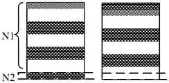
- the scanning duration T of each frame incudes a display area scanning duration T1 and a front-back porch duration T2.
- time for the scanning driving circuit to scan one row of pixels is t
- the number of rows of pixels in the display area is N1
- the number of rows of pixels corresponding to the front-back porch is N2
- the display area scanning duration T1 is equal to N1*t
- the front-back porch duration T2 is equal to N2*t that is equal to a period for which the N2 rows of the pixels are scanned
- the scanning duration of each frame T is equal to N*t
- the number of rows of pixels corresponding to the front-back porch refers to the number of rows of pixels that can be scanned by the scanning driving circuit in a period last for the front-back porch duration.
- the display panel further includes a light-emitting driving circuit 20 arranged in the non-display area 002 configured to provide the light-emitting control signal to pixels in each row during the scanning duration T of each frame.
- the light-emitting driving circuit 20 provides the light-emitting control signal to each row of pixels 301 through a light-emitting control signal line Emit.
- the light-emitting control signal has b1 (b1 is a positive integer) light-emitting cycles, and a duty cycle of an effective turn-on signal is a1.
- the light-emitting control signal provided by the light-emitting driving circuit 20 to each row of pixels has three light-emitting cycles.
- FIG. 4A to FIG. 4L illustrate schematic diagrams of images where the bright and dark stripes change during one frame.
- FIG. 4A is a schematic diagram of an image of bright and dark stripes at a moment (time) t1
- FIG. 4B is a schematic diagram of an image of bright and dark stripes at a moment t2
- FIG. 4C is a schematic diagram of an image of bright and dark stripes at a moment t3
- FIG. 4D is a schematic diagram of an image of bright and dark stripes at a moment t4
- FIG. 4E is a schematic diagram of an image of bright and dark stripes at a moment t5
- FIG. 4F is a schematic diagram of an image of bright and dark stripes at a moment t6, FIG.
- FIG. 4G is a schematic diagram of an image of bright and dark stripes at a moment t7
- FIG. 4H is a schematic diagram of an image of bright and dark stripes at a moment t8
- FIG. 4I is a schematic diagram of an image of bright and dark stripes at a moment t9
- FIG. 4J is a schematic diagram of an image of bright and dark stripes at a moment t10
- FIG. 4K is a schematic diagram of an image of bright and dark stripes at a moment a1
- FIG. 4L is a schematic diagram of an image of bright and dark stripes at a moment t12. As shown in FIGS.
- one bright stripe 401 and one adjacent dark stripe 402 constitute one bright and dark stripe 40 , which corresponds to one light-emitting cycle of the light-emitting control signal. It should be noted that, in order to clearly describe rolling of the bright and dark stripes, a filling pattern of one dark stripe is different from filling patterns of another two dark stripes in FIGS. 4A to 4L .
- the display panel further includes a touch signal driving circuit 302 arranged in the non-display area 002 , and during the display area scanning duration T1, if the number of rows of light-emitting pixel-rows in the display area 001 is fixed, the touch signal driving circuit outputs a touch signal. For example, in FIG. 4A to FIG.
- FIG. 5 is a schematic diagram of traces in a fan-out area provided by an embodiment of the present disclosure.
- an orthographic projection of a touch trace TP for transmitting touch signals on a plane of the display panel is overlapped with an orthographic projection of a constant voltage signal line PVDD for display on the plane of the display panel.
- a voltage drop of a voltage of the PVDD of the organic light-emitting display panel is stable, so that during this period, the touch trace TP transmits the touch signals, a parasitic capacitance between the TP trace and the PVDD is small, and signal interference between the touch and the display is relatively small.
- the touch driving and the display driving are performed simultaneously during the scanning duration of one frame, which increases the time for the source signal driving circuit to transmit data to each row of pixels in the display area, and can simultaneously meet the requirements of narrow steps and high-frequency display.
- the touch driving is performed during the time where the number of rows of the light-emitting pixel-rows in the display area on the display panel is fixed, and when the number of rows of the light-emitting pixel-rows in the display area is fixed, the voltage drop of the display panel in the display area is stable, and the interference of the touch and the display noise will be reduced, thereby reducing the parasitic capacitance generated when the touch and the display are driven at the same time, and improving the problem of mutual interference between the touch and the display.
- the touch signal driving circuit can output touch signals in following two cases:
- the touch signal driving circuit outputs the touch signal
- the touch signal driving circuit outputs the touch signal.
- FIG. 6A to FIG. 6L illustrate schematic diagrams of images where bright and dark stripes change with time in one frame.
- FIG. 6A is a schematic diagram of an image of bright and dark stripes at the moment t1
- FIG. 6B is a schematic diagram of an image of bright and dark stripes at the moment t2
- FIG. 6C is a schematic diagram of an image of bright and dark stripes at the moment t3
- FIG. 6D is a schematic diagram of an image of bright and dark stripes at the moment t4
- FIG. 6E is a schematic diagram of an image of bright and dark stripes at the moment t5
- FIG. 6F is a schematic diagram of an image of bright and dark stripes at the moment t6, FIG.
- FIG. 6G is a schematic diagram of an image of bright and dark stripes at the moment t7
- FIG. 6H is a schematic diagram of an image of bright and dark stripes at the moment t8
- FIG. 6I is a schematic diagram of an image of bright and dark stripes at the moment t9
- FIG. 6J is a schematic diagram of an image of bright and dark stripes at the moment t10
- FIG. 6K is a schematic diagram of an image of bright and dark stripes at the moment t11
- FIG. 6L is a schematic diagram of an image of bright and dark stripes at the moment t12.
- the number N2 of rows of pixels corresponding to the front-back porch is smaller than the number H2 of rows of pixels in one dark stripe 402 , and the number N2 of rows of pixels corresponding to the front-back porch is larger than the number H1 of rows of pixels in one bright stripe 401 .
- the total number of the bright stripes in the display area on the display panel is constant.
- the number of the rows of light-emitting pixel-rows in the display area on the display panel is fixed, and the voltage drop of the display panel in the display area is stable.
- the touch signal driving circuit can output the touch signal during the period of t2 to t3, the period of t6 to t7 and the period of t10 to t11, that is, when the number of rows of the light-emitting pixel-rows in the display area is the smallest, the touch signal driving circuit outputs the touch signal.
- the touch signal driving circuit can output the touch signal during the period of t4 to t5, the period of t8 to t9 and the period of t12 to t1, that is, when the number of rows of the light-emitting pixel-rows in the display area is the largest, the touch signal driving circuit outputs the touch signal.
- the touch signal driving circuit can output the touch signal in following two cases:
- the touch signal driving circuit outputs the touch signal
- the touch signal driving circuit outputs the touch signal.
- FIG. 7A to FIG. 7L illustrate schematic diagrams of images where bright and dark stripes change during one frame.
- FIG. 7A is a schematic diagram of an image of bright and dark stripes at the moment t1
- FIG. 7B is a schematic diagram of an image of bright and dark stripes at the moment t2
- FIG. 7C is a schematic diagram of an image of bright and dark stripes at the moment t3
- FIG. 7D is a schematic diagram of an image of bright and dark stripes at the moment t4
- FIG. 7E is a schematic diagram of an image of bright and dark stripes at the moment t5
- FIG. 7F is a schematic diagram of an image of bright and dark stripes at the moment t6
- FIG. 7G is a schematic diagram of an image of bright and dark stripes at the moment t7
- FIG. 7H is a schematic diagram of an image of bright and dark stripes at the moment t8
- FIG. 7I is a schematic diagram of an image of bright and dark stripes at the moment t9
- FIG. 7J is a schematic diagram of an image of bright and dark stripes at the moment t10
- FIG. 7K is a schematic diagram of an image of bright and dark stripes at the moment t11
- FIG. 7L is a schematic diagram of an image of bright and dark stripes at the moment t12.
- a filling pattern of one dark stripe is different from filling patterns of another two dark stripes in FIGS. 7A to 7L .
- the number N2 of rows of pixels corresponding to the front-back porch is smaller than the number H2 of rows of pixels in one dark stripe 402
- the number N2 of rows of pixels corresponding to the front-back porch is smaller than the number H1 of rows of pixels in one bright stripe 401 .
- the total number of the bright stripes in the display area on the display panel is constant.
- the number of the rows of light-emitting pixel-rows in the display area on the display panel is fixed, and the voltage drop of the display panel in the display area is stable.
- the touch signal driving circuit can output the touch signal during the period of t2 to t3, the period of t6 to t7 and the period of t10 to t11, that is, the touch signal driving circuit outputs the touch signal when the number of rows of the light-emitting pixel-rows in the display area is the smallest.
- the touch signal driving circuit can output the touch signal during the period of t4 to t5, the period of t8 to t9 and the period of t12 to t1, that is, the touch signal driving circuit outputs the touch signal when the number of rows of the light-emitting pixel-rows in the display area is the largest.
- the touch signal driving circuit can output the touch signal in following two cases:
- the touch signal driving circuit outputs the touch signal
- the touch signal driving circuit outputs the touch signal.
- FIG. 4A to FIG. 4L illustrate schematic diagrams of images where bright and dark stripes change during one frame.
- the number N2 of rows of pixels corresponding to the front-back porch is greater than the number H2 of rows of pixels in one dark stripe 402
- the number N2 of rows of pixels corresponding to the front-back porch is smaller than the number H1 of rows of pixels in one bright stripe 401 .
- FIG. 4A to FIG. 4C illustrate schematic diagrams of images where bright and dark stripes change during one frame.
- the touch signal driving circuit can output the touch signal during the period of t1 to t2, the period of t5 to t6, and the period of t9 to t10, that is, the touch signal driving circuit outputs the touch signal when the number of rows of the light-emitting pixel-rows in the display area is the smallest.
- the touch signal driving circuit can output the touch signal during the period of t3 to t4, the period of t7 to t8 and the period of t11 to t12, that is, the touch signal driving circuit outputs the touch signal when the number of rows of the light-emitting pixel-rows in the display area is the largest.
- FIG. 8A to FIG. 8T illustrate schematic diagrams of images where bright and dark stripes change with time in one frame.
- FIG. 8A is a schematic diagram of an image of bright and dark stripes at the moment t1
- FIG. 8B is a schematic diagram of an image of bright and dark stripes at the moment t2
- FIG. 8C is a schematic diagram of an image of bright and dark stripes at the moment t3
- FIG. 8D is a schematic diagram of an image of bright and dark stripes at the moment t4
- FIG. 8E is a schematic diagram of an image of bright and dark stripes at the moment t5
- FIG. 8F is a schematic diagram of an image of bright and dark stripes at the moment t6, FIG.
- FIG. 8G is a schematic diagram of an image of bright and dark stripes at the moment t7
- FIG. 8H is a schematic diagram of an image of bright and dark stripes at the moment t8
- FIG. 8I is a schematic diagram of an image of bright and dark stripes at the moment t9
- FIG. 8J is a schematic diagram of an image of bright and dark stripes at the moment t10
- FIG. 8K is a schematic diagram of an image of bright and dark stripes at the moment t11
- FIG. 8L is a schematic diagram of an image of bright and dark stripes at the moment t12
- FIG. 8M is a schematic diagram of an image of bright and dark stripes at the moment t13
- FIG. 8N is a schematic diagram of an image of bright and dark stripes at the moment t14
- FIG. 8O is a schematic diagram of an image of bright and dark stripes at the moment t15
- FIG. 8P is a schematic diagram of an image of bright and dark stripes at the moment t16
- FIG. 8Q is a schematic diagram of an image of bright and dark stripes at the moment t17
- FIG. 8R is a schematic diagram of an image of bright and dark stripes at the moment t18
- FIG. 8S is a schematic diagram of an image of bright and dark stripes at the moment t19
- FIG. 8T is a schematic diagram of an image of bright and dark stripes at the moment t20.
- the number N2 of rows of pixels corresponding to the front-back porch is larger than the number H2 of rows of pixels in one dark stripe 402 , and the number N2 of rows of pixels corresponding to the front-back porch is smaller than the number H1 of rows of pixels in one bright stripe 401 .
- FIG. 8A to FIG. 8D the number N2 of rows of pixels corresponding to the front-back porch is larger than the number H2 of rows of pixels in one dark stripe 402 , and the number N2 of rows of pixels corresponding to the front-back porch is smaller than the number H1 of rows of pixels in one bright stripe 401 .
- the total number of the bright stripes in the display area on the display panel is constant, and the voltage drop of the display panel in the display area is stable.
- the touch signal driving circuit can output the touch signal during the period of t1 to t2, the period of t5 to t6, the period of t9 to t10, the period of t13 to t14, and the period of t17 to t18, that is, the touch signal driving circuit outputs the touch signal when the number of rows of the light-emitting pixel-rows in the display area is the smallest.
- the touch signal driving circuit can output the touch signal during the period of t3 to t4, the period of t7 to t8, the period of t11 to t12, the period of t15 to t16 and the period of t19 to t20, that is, the touch signal driving circuit outputs the touch signal when the number of rows of the light-emitting pixel-rows in the display area is the largest.
- the touch signal driving circuit can output the touch signal in following two cases:
- the touch signal driving circuit outputs the touch signal
- the touch signal driving circuit outputs the touch signal.
- FIGS. 9A to 9L are schematic diagrams of images where bright and dark stripes change with time in one frame.
- FIG. 9A is a schematic diagram of an image of bright and dark stripes at the moment t1
- FIG. 9B is a schematic diagram of an image of bright and dark stripes at the moment t2
- FIG. 9C is a schematic diagram of an image of bright and dark stripes at the moment t3
- FIG. 9D is a schematic diagram of an image of bright and dark stripes at the moment t4
- FIG. 9E is a schematic diagram of an image of bright and dark stripes at the moment t5
- FIG. 9F is a schematic diagram of an image of bright and dark stripes at the moment t6, FIG.
- FIG. 9G is a schematic diagram of an image of bright and dark stripes at the moment t7
- FIG. 9H is a schematic diagram of an image of bright and dark stripes at the moment t8
- FIG. 9I is a schematic diagram of an image of bright and dark stripes at the moment t9
- FIG. 9J is a schematic diagram of an image of bright and dark stripes at the moment t10
- FIG. 9K is a schematic diagram of an image of bright and dark stripes at the moment t11
- FIG. 9L is a schematic diagram of an image of bright and dark stripes at the moment t12.
- a filling pattern of one dark stripe is different from filling patterns of another two dark stripes in FIG. 9A to FIG. 9L .
- one dark stripe formed by H2 (N/b1)*(1 ⁇ a1) rows of pixels.
- the number N2 of rows of pixels corresponding to the front-back porch is greater than the number H2 of rows of pixels in one dark stripe 402
- the number N2 of rows of pixels in the front-back porches is greater than the number H1 of rows of pixels in one bright stripe 401 .
- the total number of the bright stripes in the display area on the display panel is constant.
- the touch signal driving circuit can output the touch signal during the period of t1 to t2, the period of t5 to t6, and the period of t9 to t10, that is, the touch signal driving circuit outputs the touch signal when the number of rows of the light-emitting pixel-rows in the display area is the smallest.
- the touch signal driving circuit can output the touch signal during the period of t3 to t4, the period of t7 to t8, and the period of t11 to t12, that is, the touch signal driving circuit outputs the touch signal when the number of rows of the light-emitting pixel-rows in the display area is the largest.
- detecting the touch signal is started when the number of rows of the light-emitting pixel-rows in the display area is the smallest.
- the touch signal driving circuit outputs the touch signal within the period of t1 to t2, the period of t5 to t6, and the period of t9 to t10.
- the touch signal driving circuit can output the touch signal during a scanning duration in which the scanning driving circuit scans first to 39th rows of the pixels, a scanning duration in which the scanning driving circuit scans 156th to 195th rows of the pixels, and a scanning duration in which the scanning driving circuit scans 312nd to 351st rows of the pixels, as shown in FIG. 10 .
- touch signal driving circuit outputs touch signals and the time in which a source signal driving circuit transmits data to all rows of pixels is saved.
- FIG. 11 is a working timing sequence diagram of an organic light-emitting display panel provided by the present disclosure.
- the display area scanning duration further includes a data signal writing duration t w during which the source signal driving circuit 301 transmits data to each row of pixels, and in terms of timing sequence, the touch duration t c is located between two data signal writing durations.
- the working frequency of the display panel is 60 Hz
- the time for the source signal driving circuit to transmit data is 2.5 ⁇ s
- the duty cycle of the light-emitting control signal is 75%
- the touch signal driving circuit in order to increase the time during which touch driving is performed, can output the touch signal within time during which the number of rows of the light-emitting pixel rows in the display area is fixed.
- one light-emitting cycle a case where the number of the rows of the light-emitting pixel-rows is largest in the display area occurs once, and a case where the number of the rows of the light-emitting pixel-rows is smallest in the display area also occurs once. That is, one light-emitting cycle includes two touch durations during each of which the touch signal driving circuit outputs the touch signal, and thus b1 light-emitting cycles includes 2b1 touch durations.
- touch durations such as, the period of t1 to t2, the period of t3 to t4, the period of t5 to t6, the period of t7 to t8, the period of t9 to t10, the period of t11 to t12, the period of t14 to t14, the period of t15 to t16, the period of t17 to t18, and the period of t19 to t20 in FIG. 8A to FIG. 8T .
- the source signal driving circuit and the touch signal driving circuit are controlled by the same driver chip.
- FIG. 12 is a schematic diagram of a display device provided by an embodiment of the present disclosure.
- the display device 1 includes any one organic light-emitting display panel 01 as described above.
- the display device shown in FIG. 12 is exemplary illustrated, and the display device can be any electronic device having a display function, such as a mobile phone, a tablet computer, a notebook computer, an electronic paper book, or a television. Since the display device provided by the embodiment of the present disclosure includes the above-mentioned display panel, with this display device, by performing the touch driving and the display driving simultaneously, the time for the source signal driving circuit to transmit data to the pixels in the display area is increased, which can meet the needs of narrow steps and high-frequency display at the same time.
- the touch driving duration is within the duration where the number of rows of the light-emitting pixel-rows in the display area on the display panel is fixed, and when the number of rows of the light-emitting pixel-rows in the display area is fixed, the voltage drop of the display panel in the display area is stable, and the interference caused by noises generated by touch and the display will be reduced, thereby reducing the parasitic capacitance generated when the touch and the display are driven at the same time, and improving the problem of mutual interference between the touch and the display.
- an embodiment of the present disclosure also provides a method for driving an organic light-emitting display panel, and since the method for driving the organic light-emitting display panel solves the problem in a principle similar to that of the aforementioned organic light-emitting display panel, the implementation of the method for driving the organic light-emitting display panel can refer to the implementation of the organic light-emitting display panel, and will not be repeated herein.
- the method for driving the above organic light-emitting display panel includes: providing, by the light-emitting driving circuit, the light-emitting control signal having b1 light-emitting cycles to each row of the plurality of rows of pixels during the scanning duration of each frame; scanning, by the scanning driving circuit, each row of the plurality of rows of pixels during the scanning duration of each frame; writing, by the source signal driving circuit, source data to each row of the plurality of rows of pixels during the scanning duration of each frame, and providing, by the touch signal driving circuit, a touch driving signal to the organic light-emitting display panel during each frame; providing, by the touch signal driving circuit, the touch signal to the organic light-emitting display panel; and remaining the number of rows of light-emitting pixel-rows of the organic light-emitting display panel unchanged.
- Each of the light-emitting pixel-rows is a row of the plurality of rows of pixels, and in each light-emitting pixel-row, the pixels thereof are supplied with the effective turn-on signal of the light-emitting control signal and emit light.
- the scanning duration of one frame includes c1 touch durations, where c1 is equal to 2b1.
- the display area scanning duration further includes multiple data signal writing durations, during each of which the source signal driving circuit writes data to the display panel.
- the touch duration is located between two data signal writing durations.
- the source signal driving circuit and the touch signal driving circuit are controlled by the same driver chip.
- the touch signal driving circuit can output touch signals in following two cases:
- the touch signal driving circuit outputs the touch signal
- the touch signal driving circuit outputs the touch signal.
- the touch signal driving circuit can output touch signals in following two cases:
- the touch signal driving circuit outputs the touch signal
- the touch signal driving circuit outputs the touch signal.
- the number of rows of pixels corresponding to the front-back porch is greater than the number of rows of pixels in one dark stripe and smaller than the number of rows of pixels in one bright stripe, that is, when (N/b1)*(1 ⁇ a1) ⁇ N2 ⁇ (N/b1)*a1, the touch signal driving circuit can output touch signals in following two cases:
- the touch signal driving circuit outputs the touch signal
- the touch signal driving circuit outputs the touch signal.
- the touch signal driving circuit can output touch signals in following two cases:
- the touch signal driving circuit outputs the touch signal
- the touch signal driving circuit outputs the touch signal.
- the organic light-emitting display panel, the display device, and the method for driving the organic light-emitting display panel are provided by the present disclosure, the touch driving and the display driving are performed at the same time, which increases the time for the source signal driving circuit to transmit data to the pixels in the display area and meet the needs of narrow steps and high-frequency display at the same time.
- the touch duration is set within the duration during which the number of rows of the light-emitting pixel-rows in the display area on the display panel is fixed.
- the voltage drop of the display panel in the display area is stable, and the interference caused by noises generated by touch and the display and the display will be reduced, thereby reducing the parasitic capacitance generated when the touch and the display are driven at the same time, and improving the problem of mutual interference between the touch and the display.
Landscapes
- Engineering & Computer Science (AREA)
- Theoretical Computer Science (AREA)
- Physics & Mathematics (AREA)
- General Physics & Mathematics (AREA)
- General Engineering & Computer Science (AREA)
- Computer Hardware Design (AREA)
- Human Computer Interaction (AREA)
- Electroluminescent Light Sources (AREA)
- Control Of El Displays (AREA)
- Control Of Indicators Other Than Cathode Ray Tubes (AREA)
Abstract
Description
Claims (16)
Applications Claiming Priority (2)
| Application Number | Priority Date | Filing Date | Title |
|---|---|---|---|
| CN202011380523.5 | 2020-11-30 | ||
| CN202011380523.5A CN112735335B (en) | 2020-11-30 | 2020-11-30 | Organic light-emitting display panel, display device and driving method |
Publications (2)
| Publication Number | Publication Date |
|---|---|
| US20210216188A1 US20210216188A1 (en) | 2021-07-15 |
| US11385740B2 true US11385740B2 (en) | 2022-07-12 |
Family
ID=75598012
Family Applications (1)
| Application Number | Title | Priority Date | Filing Date |
|---|---|---|---|
| US17/213,000 Active US11385740B2 (en) | 2020-11-30 | 2021-03-25 | Organic light-emitting display panel and method for driving the same, and display device |
Country Status (2)
| Country | Link |
|---|---|
| US (1) | US11385740B2 (en) |
| CN (1) | CN112735335B (en) |
Families Citing this family (6)
| Publication number | Priority date | Publication date | Assignee | Title |
|---|---|---|---|---|
| JP2022114180A (en) * | 2021-01-26 | 2022-08-05 | シャープディスプレイテクノロジー株式会社 | Touch panel built-in display device and control method of touch panel built-in display device |
| CN113760130A (en) * | 2021-09-06 | 2021-12-07 | 合肥松豪电子科技有限公司 | TP chip scanning method avoiding noise |
| CN114141195B (en) * | 2021-12-10 | 2023-05-02 | Tcl华星光电技术有限公司 | Light emitting device driving circuit, display panel and driving method thereof |
| CN114816128B (en) * | 2022-05-30 | 2025-05-13 | 武汉华星光电半导体显示技术有限公司 | Display device and driving method thereof, and active pen |
| KR20240011919A (en) * | 2022-07-19 | 2024-01-29 | 삼성디스플레이 주식회사 | Display device and manufacturing method of the same |
| CN116027931B (en) * | 2023-03-28 | 2023-07-07 | 惠科股份有限公司 | Touch display driving circuit, driving method and touch display panel |
Citations (6)
| Publication number | Priority date | Publication date | Assignee | Title |
|---|---|---|---|---|
| CN105843442A (en) | 2016-03-15 | 2016-08-10 | 武汉华星光电技术有限公司 | Driving method used for touch display panel |
| CN107622752A (en) | 2017-09-08 | 2018-01-23 | 上海天马微电子有限公司 | O L ED display panel, driving method thereof and display device |
| CN109388269A (en) | 2017-08-11 | 2019-02-26 | 京东方科技集团股份有限公司 | Touch display panel and its driving method, touch display unit |
| CN109669583A (en) | 2019-01-04 | 2019-04-23 | 京东方科技集团股份有限公司 | Driving circuit, driving method and the touch control display apparatus of touch-control display panel |
| CN111489692A (en) | 2019-01-25 | 2020-08-04 | 上海和辉光电有限公司 | Organic light emitting diode display device and driving method thereof |
| US20210349601A1 (en) * | 2020-05-07 | 2021-11-11 | Novatek Microelectronics Corp. | Method for driving touch-and-display device, driving circuit, and touch-and-display device |
Family Cites Families (9)
| Publication number | Priority date | Publication date | Assignee | Title |
|---|---|---|---|---|
| EP2863289A1 (en) * | 2008-11-18 | 2015-04-22 | Studer Professional Audio GmbH | Input device and method of detecting a user input with an input device |
| CN101493594A (en) * | 2009-02-20 | 2009-07-29 | 天马微电子股份有限公司 | Display device with touch screen function |
| TWI469125B (en) * | 2012-08-31 | 2015-01-11 | Au Optronics Corp | Touch display apparatus and display-driving method |
| CN103926727B (en) * | 2013-12-24 | 2017-08-25 | 上海天马微电子有限公司 | Touch display panel and display device |
| CN104391600B (en) * | 2014-11-06 | 2017-11-10 | 京东方科技集团股份有限公司 | A kind of In-cell touch panel and display device |
| CN104536610B (en) * | 2014-12-31 | 2018-02-02 | 上海天马有机发光显示技术有限公司 | A kind of contact panel, touch control display apparatus and preparation method thereof |
| CN107481667B (en) * | 2017-08-25 | 2019-11-05 | 上海天马有机发光显示技术有限公司 | A kind of organic electroluminescent display panel, its driving method and display device |
| CN110322833B (en) * | 2018-03-30 | 2021-02-12 | 上海和辉光电股份有限公司 | Display driving method, method for controlling light emission of display panel and display panel |
| CN108762551B (en) * | 2018-05-16 | 2021-10-19 | 京东方科技集团股份有限公司 | Touch display panel, device and driving method thereof |
-
2020
- 2020-11-30 CN CN202011380523.5A patent/CN112735335B/en active Active
-
2021
- 2021-03-25 US US17/213,000 patent/US11385740B2/en active Active
Patent Citations (8)
| Publication number | Priority date | Publication date | Assignee | Title |
|---|---|---|---|---|
| CN105843442A (en) | 2016-03-15 | 2016-08-10 | 武汉华星光电技术有限公司 | Driving method used for touch display panel |
| CN109388269A (en) | 2017-08-11 | 2019-02-26 | 京东方科技集团股份有限公司 | Touch display panel and its driving method, touch display unit |
| US20190235663A1 (en) * | 2017-08-11 | 2019-08-01 | Boe Technology Group Co., Ltd. | Driving method for touch display panel |
| CN107622752A (en) | 2017-09-08 | 2018-01-23 | 上海天马微电子有限公司 | O L ED display panel, driving method thereof and display device |
| US20180130421A1 (en) * | 2017-09-08 | 2018-05-10 | Shanghai Tianma Micro-electronics Co., Ltd. | Organic light-emitting diode (oled) display panel, driving method thereof and display apparatus |
| CN109669583A (en) | 2019-01-04 | 2019-04-23 | 京东方科技集团股份有限公司 | Driving circuit, driving method and the touch control display apparatus of touch-control display panel |
| CN111489692A (en) | 2019-01-25 | 2020-08-04 | 上海和辉光电有限公司 | Organic light emitting diode display device and driving method thereof |
| US20210349601A1 (en) * | 2020-05-07 | 2021-11-11 | Novatek Microelectronics Corp. | Method for driving touch-and-display device, driving circuit, and touch-and-display device |
Non-Patent Citations (1)
| Title |
|---|
| State Intellectual Property Office of the People's Republic of China, First Office Action, Chinese Patent Application No. 202011380523.5, dated Sep. 14, 2021, 15 pages. |
Also Published As
| Publication number | Publication date |
|---|---|
| CN112735335B (en) | 2022-04-29 |
| CN112735335A (en) | 2021-04-30 |
| US20210216188A1 (en) | 2021-07-15 |
Similar Documents
| Publication | Publication Date | Title |
|---|---|---|
| US11385740B2 (en) | Organic light-emitting display panel and method for driving the same, and display device | |
| US10748476B2 (en) | Display panel, method for driving the same, and display device | |
| US11475818B2 (en) | Display panel having subpixels connected to different scanning lines and driving method thereof | |
| US11424297B2 (en) | Display panel having multiple display regions and display apparatus | |
| US11341926B2 (en) | Backlight module, control method therefor and display device, driving method therefor | |
| CN107742502B (en) | Display panel, display method and display device | |
| US12087247B2 (en) | Driving method of display panel, display panel, and display device driven by driving modes having different frequencies | |
| US20230096851A1 (en) | Pixel driving circuit and driving method thereof, light-emitting panel, and display device | |
| US20180047804A1 (en) | Display panel, electronic device and test method | |
| CN109215587B (en) | Display device, driving method and electronic equipment | |
| US9557840B2 (en) | Displays with intra-frame pause | |
| CN111356974A (en) | Position detection system and touch sensor | |
| US11158238B2 (en) | Display panel and driving method thereof | |
| US11804161B1 (en) | Display panel and display device | |
| CN103412673B (en) | Colored film substrate, manufacturing method of colored film substrate and touch screen | |
| US11727886B1 (en) | Display panel and drive method thereof, and display apparatus | |
| CN109697952A (en) | Display panel, control method thereof and display device | |
| CN103794176A (en) | Pixel driving circuit and driving method thereof, and display device | |
| US20190138783A1 (en) | Display panel and display device | |
| KR20220091237A (en) | Touch display device, touch circuit, and touch driving method | |
| CN113593485A (en) | Liquid crystal display device having a plurality of pixel electrodes | |
| CN109448642B (en) | Display module, driving method thereof and display device | |
| CN110910839A (en) | Control method and control system of display module | |
| US12494157B2 (en) | Driving method for display panel, and display device | |
| US11922885B2 (en) | Display panel and display driving method for display panel and display apparatus |
Legal Events
| Date | Code | Title | Description |
|---|---|---|---|
| AS | Assignment |
Owner name: SHANGHAI TIANMA AM-OLED CO., LTD., CHINA Free format text: ASSIGNMENT OF ASSIGNORS INTEREST;ASSIGNORS:CHENG, LIN;WU, YINGYING;YANG, SHUAI;AND OTHERS;REEL/FRAME:055724/0204 Effective date: 20210319 |
|
| FEPP | Fee payment procedure |
Free format text: ENTITY STATUS SET TO UNDISCOUNTED (ORIGINAL EVENT CODE: BIG.); ENTITY STATUS OF PATENT OWNER: LARGE ENTITY |
|
| STPP | Information on status: patent application and granting procedure in general |
Free format text: APPLICATION DISPATCHED FROM PREEXAM, NOT YET DOCKETED |
|
| STPP | Information on status: patent application and granting procedure in general |
Free format text: DOCKETED NEW CASE - READY FOR EXAMINATION |
|
| STPP | Information on status: patent application and granting procedure in general |
Free format text: NON FINAL ACTION MAILED |
|
| AS | Assignment |
Owner name: WUHAN TIANMA MICROELECTRONICS CO., LTD. SHANGHAI BRANCH, CHINA Free format text: ASSIGNMENT OF ASSIGNORS INTEREST;ASSIGNOR:SHANGHAI TIANMA AM-OLED CO.,LTD.;REEL/FRAME:059498/0307 Effective date: 20220301 Owner name: WUHAN TIANMA MICRO-ELECTRONICS CO., LTD., CHINA Free format text: ASSIGNMENT OF ASSIGNORS INTEREST;ASSIGNOR:SHANGHAI TIANMA AM-OLED CO.,LTD.;REEL/FRAME:059498/0307 Effective date: 20220301 Owner name: WUHAN TIANMA MICRO-ELECTRONICS CO., LTD., CHINA Free format text: ASSIGNMENT OF ASSIGNOR'S INTEREST;ASSIGNOR:SHANGHAI TIANMA AM-OLED CO.,LTD.;REEL/FRAME:059498/0307 Effective date: 20220301 Owner name: WUHAN TIANMA MICROELECTRONICS CO., LTD. SHANGHAI BRANCH, CHINA Free format text: ASSIGNMENT OF ASSIGNOR'S INTEREST;ASSIGNOR:SHANGHAI TIANMA AM-OLED CO.,LTD.;REEL/FRAME:059498/0307 Effective date: 20220301 |
|
| STPP | Information on status: patent application and granting procedure in general |
Free format text: RESPONSE TO NON-FINAL OFFICE ACTION ENTERED AND FORWARDED TO EXAMINER |
|
| STPP | Information on status: patent application and granting procedure in general |
Free format text: NOTICE OF ALLOWANCE MAILED -- APPLICATION RECEIVED IN OFFICE OF PUBLICATIONS |
|
| STPP | Information on status: patent application and granting procedure in general |
Free format text: PUBLICATIONS -- ISSUE FEE PAYMENT RECEIVED |
|
| STPP | Information on status: patent application and granting procedure in general |
Free format text: PUBLICATIONS -- ISSUE FEE PAYMENT VERIFIED |
|
| STCF | Information on status: patent grant |
Free format text: PATENTED CASE |
|
| MAFP | Maintenance fee payment |
Free format text: PAYMENT OF MAINTENANCE FEE, 4TH YEAR, LARGE ENTITY (ORIGINAL EVENT CODE: M1551); ENTITY STATUS OF PATENT OWNER: LARGE ENTITY Year of fee payment: 4 |