US11380745B2 - Display panel including thin film transistors having different semiconductor materials from each other - Google Patents
Display panel including thin film transistors having different semiconductor materials from each other Download PDFInfo
- Publication number
- US11380745B2 US11380745B2 US16/294,193 US201916294193A US11380745B2 US 11380745 B2 US11380745 B2 US 11380745B2 US 201916294193 A US201916294193 A US 201916294193A US 11380745 B2 US11380745 B2 US 11380745B2
- Authority
- US
- United States
- Prior art keywords
- electrode
- insulating layer
- layer
- disposed
- semiconductor pattern
- Prior art date
- Legal status (The legal status is an assumption and is not a legal conclusion. Google has not performed a legal analysis and makes no representation as to the accuracy of the status listed.)
- Active, expires
Links
Images


Classifications
-
- H—ELECTRICITY
- H10—SEMICONDUCTOR DEVICES; ELECTRIC SOLID-STATE DEVICES NOT OTHERWISE PROVIDED FOR
- H10D—INORGANIC ELECTRIC SEMICONDUCTOR DEVICES
- H10D86/00—Integrated devices formed in or on insulating or conducting substrates, e.g. formed in silicon-on-insulator [SOI] substrates or on stainless steel or glass substrates
- H10D86/40—Integrated devices formed in or on insulating or conducting substrates, e.g. formed in silicon-on-insulator [SOI] substrates or on stainless steel or glass substrates characterised by multiple TFTs
- H10D86/421—Integrated devices formed in or on insulating or conducting substrates, e.g. formed in silicon-on-insulator [SOI] substrates or on stainless steel or glass substrates characterised by multiple TFTs having a particular composition, shape or crystalline structure of the active layer
-
- H01L27/3248—
-
- H—ELECTRICITY
- H10—SEMICONDUCTOR DEVICES; ELECTRIC SOLID-STATE DEVICES NOT OTHERWISE PROVIDED FOR
- H10D—INORGANIC ELECTRIC SEMICONDUCTOR DEVICES
- H10D86/00—Integrated devices formed in or on insulating or conducting substrates, e.g. formed in silicon-on-insulator [SOI] substrates or on stainless steel or glass substrates
- H10D86/40—Integrated devices formed in or on insulating or conducting substrates, e.g. formed in silicon-on-insulator [SOI] substrates or on stainless steel or glass substrates characterised by multiple TFTs
- H10D86/421—Integrated devices formed in or on insulating or conducting substrates, e.g. formed in silicon-on-insulator [SOI] substrates or on stainless steel or glass substrates characterised by multiple TFTs having a particular composition, shape or crystalline structure of the active layer
- H10D86/423—Integrated devices formed in or on insulating or conducting substrates, e.g. formed in silicon-on-insulator [SOI] substrates or on stainless steel or glass substrates characterised by multiple TFTs having a particular composition, shape or crystalline structure of the active layer comprising semiconductor materials not belonging to the Group IV, e.g. InGaZnO
-
- G—PHYSICS
- G09—EDUCATION; CRYPTOGRAPHY; DISPLAY; ADVERTISING; SEALS
- G09G—ARRANGEMENTS OR CIRCUITS FOR CONTROL OF INDICATING DEVICES USING STATIC MEANS TO PRESENT VARIABLE INFORMATION
- G09G3/00—Control arrangements or circuits, of interest only in connection with visual indicators other than cathode-ray tubes
- G09G3/20—Control arrangements or circuits, of interest only in connection with visual indicators other than cathode-ray tubes for presentation of an assembly of a number of characters, e.g. a page, by composing the assembly by combination of individual elements arranged in a matrix no fixed position being assigned to or needed to be assigned to the individual characters or partial characters
- G09G3/22—Control arrangements or circuits, of interest only in connection with visual indicators other than cathode-ray tubes for presentation of an assembly of a number of characters, e.g. a page, by composing the assembly by combination of individual elements arranged in a matrix no fixed position being assigned to or needed to be assigned to the individual characters or partial characters using controlled light sources
- G09G3/30—Control arrangements or circuits, of interest only in connection with visual indicators other than cathode-ray tubes for presentation of an assembly of a number of characters, e.g. a page, by composing the assembly by combination of individual elements arranged in a matrix no fixed position being assigned to or needed to be assigned to the individual characters or partial characters using controlled light sources using electroluminescent panels
- G09G3/32—Control arrangements or circuits, of interest only in connection with visual indicators other than cathode-ray tubes for presentation of an assembly of a number of characters, e.g. a page, by composing the assembly by combination of individual elements arranged in a matrix no fixed position being assigned to or needed to be assigned to the individual characters or partial characters using controlled light sources using electroluminescent panels semiconductive, e.g. using light-emitting diodes [LED]
- G09G3/3208—Control arrangements or circuits, of interest only in connection with visual indicators other than cathode-ray tubes for presentation of an assembly of a number of characters, e.g. a page, by composing the assembly by combination of individual elements arranged in a matrix no fixed position being assigned to or needed to be assigned to the individual characters or partial characters using controlled light sources using electroluminescent panels semiconductive, e.g. using light-emitting diodes [LED] organic, e.g. using organic light-emitting diodes [OLED]
- G09G3/3225—Control arrangements or circuits, of interest only in connection with visual indicators other than cathode-ray tubes for presentation of an assembly of a number of characters, e.g. a page, by composing the assembly by combination of individual elements arranged in a matrix no fixed position being assigned to or needed to be assigned to the individual characters or partial characters using controlled light sources using electroluminescent panels semiconductive, e.g. using light-emitting diodes [LED] organic, e.g. using organic light-emitting diodes [OLED] using an active matrix
- G09G3/3233—Control arrangements or circuits, of interest only in connection with visual indicators other than cathode-ray tubes for presentation of an assembly of a number of characters, e.g. a page, by composing the assembly by combination of individual elements arranged in a matrix no fixed position being assigned to or needed to be assigned to the individual characters or partial characters using controlled light sources using electroluminescent panels semiconductive, e.g. using light-emitting diodes [LED] organic, e.g. using organic light-emitting diodes [OLED] using an active matrix with pixel circuitry controlling the current through the light-emitting element
-
- H01L27/1222—
-
- H01L27/3258—
-
- H01L27/3262—
-
- H01L51/5203—
-
- H—ELECTRICITY
- H10—SEMICONDUCTOR DEVICES; ELECTRIC SOLID-STATE DEVICES NOT OTHERWISE PROVIDED FOR
- H10D—INORGANIC ELECTRIC SEMICONDUCTOR DEVICES
- H10D30/00—Field-effect transistors [FET]
- H10D30/01—Manufacture or treatment
- H10D30/021—Manufacture or treatment of FETs having insulated gates [IGFET]
- H10D30/031—Manufacture or treatment of FETs having insulated gates [IGFET] of thin-film transistors [TFT]
- H10D30/0312—Manufacture or treatment of FETs having insulated gates [IGFET] of thin-film transistors [TFT] characterised by the gate electrodes
- H10D30/0314—Manufacture or treatment of FETs having insulated gates [IGFET] of thin-film transistors [TFT] characterised by the gate electrodes of lateral top-gate TFTs comprising only a single gate
-
- H—ELECTRICITY
- H10—SEMICONDUCTOR DEVICES; ELECTRIC SOLID-STATE DEVICES NOT OTHERWISE PROVIDED FOR
- H10D—INORGANIC ELECTRIC SEMICONDUCTOR DEVICES
- H10D30/00—Field-effect transistors [FET]
- H10D30/01—Manufacture or treatment
- H10D30/021—Manufacture or treatment of FETs having insulated gates [IGFET]
- H10D30/031—Manufacture or treatment of FETs having insulated gates [IGFET] of thin-film transistors [TFT]
- H10D30/0321—Manufacture or treatment of FETs having insulated gates [IGFET] of thin-film transistors [TFT] comprising silicon, e.g. amorphous silicon or polysilicon
-
- H—ELECTRICITY
- H10—SEMICONDUCTOR DEVICES; ELECTRIC SOLID-STATE DEVICES NOT OTHERWISE PROVIDED FOR
- H10D—INORGANIC ELECTRIC SEMICONDUCTOR DEVICES
- H10D30/00—Field-effect transistors [FET]
- H10D30/60—Insulated-gate field-effect transistors [IGFET]
- H10D30/67—Thin-film transistors [TFT]
- H10D30/6729—Thin-film transistors [TFT] characterised by the electrodes
- H10D30/6737—Thin-film transistors [TFT] characterised by the electrodes characterised by the electrode materials
- H10D30/6739—Conductor-insulator-semiconductor electrodes
-
- H—ELECTRICITY
- H10—SEMICONDUCTOR DEVICES; ELECTRIC SOLID-STATE DEVICES NOT OTHERWISE PROVIDED FOR
- H10K—ORGANIC ELECTRIC SOLID-STATE DEVICES
- H10K50/00—Organic light-emitting devices
- H10K50/80—Constructional details
- H10K50/805—Electrodes
-
- H—ELECTRICITY
- H10—SEMICONDUCTOR DEVICES; ELECTRIC SOLID-STATE DEVICES NOT OTHERWISE PROVIDED FOR
- H10K—ORGANIC ELECTRIC SOLID-STATE DEVICES
- H10K59/00—Integrated devices, or assemblies of multiple devices, comprising at least one organic light-emitting element covered by group H10K50/00
- H10K59/10—OLED displays
- H10K59/12—Active-matrix OLED [AMOLED] displays
- H10K59/1201—Manufacture or treatment
-
- H—ELECTRICITY
- H10—SEMICONDUCTOR DEVICES; ELECTRIC SOLID-STATE DEVICES NOT OTHERWISE PROVIDED FOR
- H10K—ORGANIC ELECTRIC SOLID-STATE DEVICES
- H10K59/00—Integrated devices, or assemblies of multiple devices, comprising at least one organic light-emitting element covered by group H10K50/00
- H10K59/10—OLED displays
- H10K59/12—Active-matrix OLED [AMOLED] displays
- H10K59/121—Active-matrix OLED [AMOLED] displays characterised by the geometry or disposition of pixel elements
- H10K59/1213—Active-matrix OLED [AMOLED] displays characterised by the geometry or disposition of pixel elements the pixel elements being TFTs
-
- H—ELECTRICITY
- H10—SEMICONDUCTOR DEVICES; ELECTRIC SOLID-STATE DEVICES NOT OTHERWISE PROVIDED FOR
- H10K—ORGANIC ELECTRIC SOLID-STATE DEVICES
- H10K59/00—Integrated devices, or assemblies of multiple devices, comprising at least one organic light-emitting element covered by group H10K50/00
- H10K59/10—OLED displays
- H10K59/12—Active-matrix OLED [AMOLED] displays
- H10K59/123—Connection of the pixel electrodes to the thin film transistors [TFT]
-
- H—ELECTRICITY
- H10—SEMICONDUCTOR DEVICES; ELECTRIC SOLID-STATE DEVICES NOT OTHERWISE PROVIDED FOR
- H10K—ORGANIC ELECTRIC SOLID-STATE DEVICES
- H10K59/00—Integrated devices, or assemblies of multiple devices, comprising at least one organic light-emitting element covered by group H10K50/00
- H10K59/10—OLED displays
- H10K59/12—Active-matrix OLED [AMOLED] displays
- H10K59/124—Insulating layers formed between TFT elements and OLED elements
-
- G—PHYSICS
- G09—EDUCATION; CRYPTOGRAPHY; DISPLAY; ADVERTISING; SEALS
- G09G—ARRANGEMENTS OR CIRCUITS FOR CONTROL OF INDICATING DEVICES USING STATIC MEANS TO PRESENT VARIABLE INFORMATION
- G09G2300/00—Aspects of the constitution of display devices
- G09G2300/04—Structural and physical details of display devices
- G09G2300/0421—Structural details of the set of electrodes
- G09G2300/0426—Layout of electrodes and connections
-
- G—PHYSICS
- G09—EDUCATION; CRYPTOGRAPHY; DISPLAY; ADVERTISING; SEALS
- G09G—ARRANGEMENTS OR CIRCUITS FOR CONTROL OF INDICATING DEVICES USING STATIC MEANS TO PRESENT VARIABLE INFORMATION
- G09G2300/00—Aspects of the constitution of display devices
- G09G2300/08—Active matrix structure, i.e. with use of active elements, inclusive of non-linear two terminal elements, in the pixels together with light emitting or modulating elements
- G09G2300/0809—Several active elements per pixel in active matrix panels
- G09G2300/0842—Several active elements per pixel in active matrix panels forming a memory circuit, e.g. a dynamic memory with one capacitor
-
- G—PHYSICS
- G09—EDUCATION; CRYPTOGRAPHY; DISPLAY; ADVERTISING; SEALS
- G09G—ARRANGEMENTS OR CIRCUITS FOR CONTROL OF INDICATING DEVICES USING STATIC MEANS TO PRESENT VARIABLE INFORMATION
- G09G3/00—Control arrangements or circuits, of interest only in connection with visual indicators other than cathode-ray tubes
- G09G3/20—Control arrangements or circuits, of interest only in connection with visual indicators other than cathode-ray tubes for presentation of an assembly of a number of characters, e.g. a page, by composing the assembly by combination of individual elements arranged in a matrix no fixed position being assigned to or needed to be assigned to the individual characters or partial characters
- G09G3/22—Control arrangements or circuits, of interest only in connection with visual indicators other than cathode-ray tubes for presentation of an assembly of a number of characters, e.g. a page, by composing the assembly by combination of individual elements arranged in a matrix no fixed position being assigned to or needed to be assigned to the individual characters or partial characters using controlled light sources
- G09G3/30—Control arrangements or circuits, of interest only in connection with visual indicators other than cathode-ray tubes for presentation of an assembly of a number of characters, e.g. a page, by composing the assembly by combination of individual elements arranged in a matrix no fixed position being assigned to or needed to be assigned to the individual characters or partial characters using controlled light sources using electroluminescent panels
- G09G3/32—Control arrangements or circuits, of interest only in connection with visual indicators other than cathode-ray tubes for presentation of an assembly of a number of characters, e.g. a page, by composing the assembly by combination of individual elements arranged in a matrix no fixed position being assigned to or needed to be assigned to the individual characters or partial characters using controlled light sources using electroluminescent panels semiconductive, e.g. using light-emitting diodes [LED]
- G09G3/3208—Control arrangements or circuits, of interest only in connection with visual indicators other than cathode-ray tubes for presentation of an assembly of a number of characters, e.g. a page, by composing the assembly by combination of individual elements arranged in a matrix no fixed position being assigned to or needed to be assigned to the individual characters or partial characters using controlled light sources using electroluminescent panels semiconductive, e.g. using light-emitting diodes [LED] organic, e.g. using organic light-emitting diodes [OLED]
- G09G3/3225—Control arrangements or circuits, of interest only in connection with visual indicators other than cathode-ray tubes for presentation of an assembly of a number of characters, e.g. a page, by composing the assembly by combination of individual elements arranged in a matrix no fixed position being assigned to or needed to be assigned to the individual characters or partial characters using controlled light sources using electroluminescent panels semiconductive, e.g. using light-emitting diodes [LED] organic, e.g. using organic light-emitting diodes [OLED] using an active matrix
-
- H01L2227/323—
-
- H01L27/1225—
-
- H01L27/1251—
-
- H01L27/1288—
-
- H01L29/78675—
-
- H01L29/7869—
-
- H—ELECTRICITY
- H10—SEMICONDUCTOR DEVICES; ELECTRIC SOLID-STATE DEVICES NOT OTHERWISE PROVIDED FOR
- H10D—INORGANIC ELECTRIC SEMICONDUCTOR DEVICES
- H10D30/00—Field-effect transistors [FET]
- H10D30/60—Insulated-gate field-effect transistors [IGFET]
- H10D30/67—Thin-film transistors [TFT]
- H10D30/674—Thin-film transistors [TFT] characterised by the active materials
- H10D30/6755—Oxide semiconductors, e.g. zinc oxide, copper aluminium oxide or cadmium stannate
-
- H—ELECTRICITY
- H10—SEMICONDUCTOR DEVICES; ELECTRIC SOLID-STATE DEVICES NOT OTHERWISE PROVIDED FOR
- H10D—INORGANIC ELECTRIC SEMICONDUCTOR DEVICES
- H10D86/00—Integrated devices formed in or on insulating or conducting substrates, e.g. formed in silicon-on-insulator [SOI] substrates or on stainless steel or glass substrates
- H10D86/40—Integrated devices formed in or on insulating or conducting substrates, e.g. formed in silicon-on-insulator [SOI] substrates or on stainless steel or glass substrates characterised by multiple TFTs
- H10D86/60—Integrated devices formed in or on insulating or conducting substrates, e.g. formed in silicon-on-insulator [SOI] substrates or on stainless steel or glass substrates characterised by multiple TFTs wherein the TFTs are in active matrices
Definitions
- Exemplary embodiments of the present invention relate to a display panel, and more particularly, to a display panel including two semiconductor materials and a method of manufacturing the same.
- Each of the pixels may include a pixel driving circuit and a display element connected to the pixel driving circuit.
- the pixel driving circuit may include at least one thin film transistor and a capacitor. The thin film transistor and the capacitor of the pixel driving circuit may control the display element in response to the electrical signal provided from the driving circuit.
- An exemplary embodiment of the present invention provides a display panel having increased process reliability and a method of manufacturing the same.
- a display panel includes a base layer and a first thin film transistor disposed on the base layer and including a silicon semiconductor pattern.
- a first control electrode is spaced apart from the silicon semiconductor pattern.
- a first input electrode is connected to a first side of the silicon semiconductor pattern.
- a first output electrode is connected to a second side of the silicon semiconductor pattern.
- a second thin film transistor is disposed on the base layer.
- the second thin film transistor includes an oxide semiconductor pattern.
- a second control electrode is spaced apart from the oxide semiconductor pattern.
- a second input electrode is connected to a first side of the oxide semiconductor pattern.
- a second output electrode is connected to a second side of the oxide semiconductor pattern.
- An organic light emitting diode includes a first electrode connected to the first thin film transistor.
- a second electrode is disposed on the first electrode.
- An emission layer is disposed between the first electrode and the second electrode.
- a first insulating layer is disposed between the organic light emitting diode and the silicon semiconductor pattern.
- the first insulating layer is disposed on the silicon semiconductor pattern.
- the first insulating layer includes a plurality of openings exposing the first side and the second side of the silicon semiconductor pattern, respectively.
- the first input electrode and the first output electrode are each positioned in an opening of the plurality of openings, respectively.
- the first input electrode and the first output electrode may be disposed on a layer different from a layer on which the second input electrode and the second output electrode are disposed.
- the display panel may include a first connection electrode connected to the first input electrode, and a second connection electrode disposed between the first electrode and the first output electrode and disposed on a same layer as the first connection electrode.
- the second connection electrode may electrically connect the first output electrode to the first electrode.
- the first connection electrode and the second connection electrode may be disposed on a same layer as the second input electrode and the second output electrode.
- the first input electrode and the first output electrode may include a different material from that of the second input electrode and the second output electrode.
- the display panel may include a bridge electrode disposed between the first electrode and the second connection electrode and connected to the first electrode and the second connection electrode.
- the bridge electrode may have a resistance lower than a resistance of the second connection electrode.
- the display panel may include a second insulating layer disposed between the first insulating layer and the first electrode, and an upper electrode disposed on the second insulating layer.
- the first control electrode may be disposed between the first insulating layer and the second insulating layer, and the upper electrode may overlap with the first control electrode when viewed in a plan view.
- the upper electrode and the first control electrode may receive a same voltage.
- thicknesses of the first input electrode and the first output electrode may be substantially equal to a thickness of the first insulating layer.
- side surfaces of the first input electrode and the first output electrode may have inclined shapes when viewed in a cross-sectional view.
- side surfaces of the first input electrode and the first output electrode need not overlap with the first insulating layer when viewed in a plan view.
- the first input electrode and the first output electrode may substantially completely fill the openings, respectively.
- the first insulating layer may include a plurality of openings exposing a first side and a second side of the oxide semiconductor pattern, respectively.
- the oxide semiconductor pattern may be disposed on a same layer as the silicon semiconductor pattern, and the second input electrode and the second output electrode may each be positioned in an opening of the plurality of openings exposing the first side and the second side of the oxide semiconductor pattern, respectively.
- a display panel includes a base layer and a thin film transistor disposed on the base layer.
- the thin film transistor includes a silicon semiconductor pattern.
- a control electrode is spaced apart from the silicon semiconductor pattern.
- An input electrode is connected to a first side of the silicon semiconductor pattern.
- An output electrode is connected to a second side of the silicon semiconductor pattern.
- a first insulating layer is disposed directly on the silicon semiconductor pattern.
- the first insulating layer includes a plurality of openings directly exposing the first side and the second side of the silicon semiconductor pattern, respectively.
- a second insulating layer is disposed on the first insulating layer and the thin film transistor.
- An organic light emitting diode includes a first electrode disposed on the second insulating layer and connected to the thin film transistor, a second electrode disposed on the first electrode, and an emission layer disposed between the first electrode and the second electrode.
- a connection electrode is disposed between the second insulating layer and the first electrode. The connection electrode penetrates the second insulating layer to electrically connect the first electrode and the output electrode.
- the input electrode and the output electrode are each disposed in an opening of the plurality of openings, respectively, to form the same layer with the first insulating layer on the silicon semiconductor pattern.
- top surfaces of the input electrode and the output electrode may be substantially coplanar with a top surface of the first insulating layer.
- the display panel may include a third insulating layer disposed on the second insulating layer and the connection electrode.
- a bridge electrode may penetrate the third insulating layer to electrically connect the first electrode and the connection electrode.
- the bridge electrode may have a resistance lower than a resistance of the connection electrode.
- control electrode may overlap with the silicon semiconductor pattern and may be disposed under the first insulating layer.
- the output electrode may be formed of a different material from that of the connection electrode.
- the output electrode, the connection electrode and the bridge electrode may all be aligned with each other along a direction orthogonal to an upper surface of the base layer.
- FIG. 1 is a perspective view of a display panel according to an exemplary embodiment of the present invention
- FIG. 2 is a plan view of a display panel according to an exemplary embodiment of the present invention.
- FIG. 3 is an equivalent circuit diagram of a pixel according to an exemplary embodiment of the present invention.
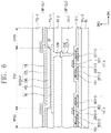
- FIG. 4 is a cross-sectional view of a portion of a pixel according to an exemplary embodiment of the present invention.
- FIG. 5 is a cross-sectional view of a portion of a pixel according to an exemplary embodiment of the present invention.
- FIG. 6 is a cross-sectional view of a portion of a pixel according to an exemplary embodiment of the present invention.
- FIG. 7 is a cross-sectional view of a portion of a pixel according to an exemplary embodiment of the present invention.
- FIG. 8 is a cross-sectional view of a portion of a pixel according to an exemplary embodiment of the present invention.
- FIGS. 9A, 9B, 9C, 9D, 9E, 9F, 9G, 9H, 9I, 9J, 9K and 9L are cross-sectional views of a method of manufacturing a display panel, according to an exemplary embodiment of the present invention.
- a component such as a layer, a film, a region, or a plate
- the component may be directly on the other component or intervening components may be present.
- spatially relative terms such as “beneath”, “below”, “lower”, “above”, or “upper” may be used herein for clarity of description to describe one element or feature's relationship to another element(s) or feature(s) as described with reference to the figures. It will be understood that the spatially relative terms are intended to encompass different orientations of the device in use or operation in addition to the orientation depicted in the figures. For example, a described device may be otherwise oriented (e.g., rotated 90 degrees or at other orientations) and the spatially relative descriptors used herein interpreted accordingly.
- FIG. 1 is a perspective view of a display panel according to an exemplary embodiment of the present invention.
- FIG. 2 is a plan view of a display panel according to an exemplary embodiment of the present invention.
- a front surface DP-FS of a display panel DP may extend along a plane defined by a first direction DR 1 and a second direction DR 2 .
- the first direction DR 1 may be perpendicular to the second direction DR 2 .
- the first direction DR 1 and the second direction DR 2 may define a plane along which the display panel extends.
- a third direction DR 3 may be perpendicular to the first and second directions DR 1 and DR 2 .
- the third direction DR 3 may be orthogonal to a plane extending in the first and second directions DR 1 and DR 2 .
- a normal direction of the front surface DP-FS of the display panel DP (e.g., a thickness direction of the display panel DP) may be indicated by the third direction DR 3 .
- a top surface (e.g., or a front surface) and a bottom surface (e.g., or a rear surface) of each of layers included in the display panel DP may be defined by the third direction DR 3 .
- the display panel DP may include a display area DP-DA and a non-display area DP-NDA in the front surface DP-FS. Pixels PX may be disposed in the display area DP-DA and the non-display area DP-NDA may be adjacent to the display area DP-DA.
- the display area DP-DA may include a plurality of pixels PX. As an example, the pixels PX may be spaced apart from each other or may be immediately adjacent to each other.
- the pixels PX may be arranged in a plurality of rows and columns on or above an underlying substrate. Thus, the pixels PX may be arranged in a matrix configuration.
- the display area DP-DA may have one of various shapes.
- the display area DP-DA may have a quadrilateral shape (e.g., a rectangular shape or a square shape).
- the display area DP-DA may have a circular shape.
- the non-display area DP-NDA may be adjacent to the display area DP-DA.
- the non-display area DP-NDA may surround the display area DP-DA when viewed in a plan view.
- the non-display region DP-NDA may be arranged at four sides of the display region DP-DA in a plan view (e.g., along the third direction DR 3 ); however, exemplary embodiments of the present invention are not limited thereto.
- the non-display region DP-NDA may be arranged at less than four sides (e.g., three sides) of the display region DP-DA in a plan view.
- the shapes of the display area DP-DA and the non-display area DP-NDA may be variously modified, as desired.
- the non-display area DP-NDA may be disposed at only one or both sides of the display area DP-DA.
- FIG. 2 schematically illustrates the connection relationship of the pixels PX, a driving circuit GDC and signal lines SGL.
- FIG. 3 is an equivalent circuit diagram of a pixel according to an exemplary embodiment of the present invention.
- FIG. 4 is a cross-sectional view of a portion of a pixel according to an exemplary embodiment of the present invention.
- the display panel DP may include a driving circuit GDC, a plurality of signal lines SGL, a plurality of signal pads DP-PD, and a plurality of the pixels PX.
- the pixels PX may be divided into a plurality of groups on the basis of colors of lights emitted from the pixels PX.
- the pixels PX may include red pixels, green pixels, and blue pixels.
- the pixels PX may further include white pixels.
- the driving circuit GDC may include a scan driving circuit.
- the scan driving circuit may generate a plurality of scan signals and may sequentially output the scan signals to a plurality of scan lines GL.
- the scan driving circuit may further output other control signals to pixel driving circuits of the pixels PX.
- the scan driving circuit may be formed together with the pixel driving circuits of the pixels PX by a same process.
- the signal lines SGL may include scan lines GL, data lines DL, a power line PL, and a control signal line CSL.
- Each of the scan lines GL may be connected to corresponding ones of the pixels PX, and each of the data lines DL may be connected to corresponding ones of the pixels PX.
- the power line PL may be connected to the pixels PX.
- the control signal line CSL may provide control signals to the scan driving circuit.
- Each of the signal pads DP-PD may be connected to a corresponding one of the signal lines SGL.
- a circuit board may be electrically connected to the display panel D.
- the circuit board may be a rigid circuit board or a flexible circuit board.
- a driving chip may be mounted on the circuit board.
- the driving chip may be mounted on the display panel DP.
- the design of the signal lines SGL may be changed.
- the driving chip may be connected to the data lines DL, and additional signal lines connecting the driving chip to the signal pads DP-PD may be disposed.
- one scan line GL, one data line DL, the power line PL, and the pixel PX connected to lines GL, DL and PL may be provided.
- the pixel PX may include an organic light emitting diode or a quantum-dot light emitting diode as a light emitting element.
- An emission layer of the organic light emitting diode may include an organic light emitting material.
- An emission layer of the quantum-dot light emitting diode may include quantum dots and/or quantum rods.
- the pixel PX corresponding to an organic light emitting pixel will be described in more detail below as an example; however, exemplary embodiments of the present invention are not limited thereto.
- the pixel PX may include an organic light emitting diode OLED and a pixel driving circuit for driving the organic light emitting diode OLED.
- the organic light emitting diode OLED may be a front surface light emitting type diode or a rear surface light emitting type diode.
- the pixel driving circuit may include a first thin film transistor T 1 (e.g., which may be a driving transistor), a second thin film transistor T 2 (e.g., which may be a switching transistor), and a capacitor Cst.
- a first power source voltage ELVDD may be provided to a terminal of the organic light emitting diode OLED through the first thin film transistor T 1
- a second power source voltage ELVSS may be provided to another terminal of the organic light emitting diode OLED.
- the second power source voltage ELVSS may be lower than the first power source voltage ELVDD.
- the first thin film transistor T 1 may be connected to the organic light emitting diode OLED.
- the first thin film transistor T 1 may control a driving current flowing through the organic light emitting diode OLED in response to the amount of charges stored in the capacitor Cst.
- the second thin film transistor T 2 may output a data signal of the data line DL in response to a scan signal applied to the scan line GL.
- the capacitor Cst may be charged with a voltage corresponding to the data signal received from the second thin film transistor T 2 .
- the configuration of the pixel PX is not limited to the examples described above (e.g., with respect to FIG. 3 ) but may be variously modified, as desired.
- the pixel driving circuit for controlling the organic light emitting diode OLED may include three or more thin film transistors.
- the organic light emitting diode OLED may be connected between the power line PL and the second thin film transistor T 2 .
- FIG. 4 illustrates a cross-sectional view corresponding to the first thin film transistor T 1 , the second thin film transistor T 2 and the organic light emitting diode OLED, which may be included in the pixel PX.
- the display panel DP may include a base layer BL, a circuit element layer DP-CL, and a display element layer DP-EL.
- the display panel DP may further include functional layers such as an anti-reflection layer and/or a refractive index adjusting layer.
- the circuit element layer DP-CL may include the first thin film transistor T 1 , the second thin film transistor T 2 , a plurality of insulating layers 10 , 20 , 30 , 40 , 50 and 60 , an upper electrode DE, connection electrodes CL 1 and CL 2 , and a bridge electrode CNE.
- the circuit element layer DP-CL may be formed through coating and/or deposition processes of forming an insulating layer, a semiconductor layer and a conductive layer and processes of patterning the insulating layer, the semiconductor layer and the conductive layer using photolithography processes.
- Each of the insulating layers 10 , 20 , 30 , 40 , 50 and 60 may include an organic layer and/or an inorganic layer.
- the display element layer DP-EL may include the organic light emitting diode OLED, a pixel defining layer PDL, and a thin film encapsulation layer TFE.
- the first thin film transistor T 1 , the second thin film transistor T 2 and the capacitor Cst may be disposed on the base layer BL.
- the base layer BL may include a synthetic resin film.
- the synthetic resin film may include a thermosetting resin.
- the synthetic resin film may be a polyimide-based resin film.
- exemplary embodiments of the present invention are not limited to a synthetic resin film including a particular material.
- the synthetic resin film may include at least one of an acrylic-based resin, a methacrylic-based resin, polyisoprene, a vinyl-based resin, an epoxy-based resin, a urethane-based resin, a cellulose-based resin, a siloxane-based resin, a polyamide-based resin, or a perylene-based resin.
- the base layer BL may include a glass substrate, a metal substrate, or an organic/inorganic composite material substrate.
- An inorganic layer BFL may be disposed on a top surface of the base layer BL (e.g., a surface of the base layer BL facing the first thin film transistor T 1 ).
- the inorganic layer BFL may include a barrier layer and/or a buffer layer.
- the inorganic layer BFL may include at least one of aluminum oxide, titanium oxide, silicon oxide, silicon oxynitride, zirconium oxide, or hafnium oxide.
- the inorganic layer BFL may have a multi-layered structure.
- the multi-layered inorganic layer BFL may have the barrier layer and the buffer layer, as described above.
- the barrier layer and the buffer layer may be selectively disposed.
- the inorganic layer BFL may have a single layer structure.
- the barrier layer may prevent a foreign material from permeating from the outside.
- the barrier layer may include a silicon oxide layer and a silicon nitride layer.
- the silicon oxide layer and the silicon nitride layer may be alternately stacked.
- the silicon oxide layer and the silicon nitride layer may be alternately and repeatedly stacked.
- the buffer layer may increase bonding strength between components disposed on and under the buffer layer.
- the buffer layer may include a silicon oxide layer and a silicon nitride layer.
- the silicon oxide layer and the silicon nitride layer may be alternately stacked.
- the silicon oxide layer and the silicon nitride layer may be alternately and repeatedly stacked.
- the first thin film transistor T 1 may include a first input electrode SE 1 , a first output electrode DE 1 , a first control electrode GE 1 , and a first semiconductor pattern OSP 1 .
- the second thin film transistor T 2 may include a second input electrode SE 2 , a second output electrode DE 2 , a second control electrode GE 2 , and a second semiconductor pattern OSP 2 .
- the first semiconductor pattern OSP 1 may be disposed on the inorganic layer BFL.
- the first semiconductor pattern OSP 1 may be in direct contact with the inorganic layer BFL.
- the first semiconductor pattern OSP 1 may include a crystalline semiconductor material.
- the first semiconductor pattern OSP 1 may include a poly-crystalline semiconductor material such as poly-crystalline silicon.
- the first semiconductor pattern OSP 1 may be interchangeably referred to herein as a silicon semiconductor pattern. Since the poly-crystalline silicon layer has a high field effect mobility, it may be applied to a relatively high-speed operation circuit. Thus, performance speed and reliability of the display panel DP may be increased.
- the first semiconductor pattern OSP 1 may include amorphous silicon.
- the first semiconductor pattern OSP 1 may include an input region (e.g., or a first portion), an output region (e.g., or a second portion), and a channel region (e.g., or a third portion) defined between the input region and the output region.
- the input region and the output region may have slanted side surfaces.
- the channel region of the first semiconductor pattern OSP 1 may be defined to overlap with the first control electrode GE 1 (e.g., along the third direction DR 3 ).
- the input region and the output region may be doped with dopants and may have conductivity higher than that of the channel region.
- the input region and the output region may be doped with N-type dopants.
- the first thin film transistor T 1 may be an N-type transistor.
- exemplary embodiments of the present invention are not limited thereto.
- the first thin film transistor T 1 may be a P-type transistor.
- a first insulating layer 10 may be disposed on the inorganic layer BFL.
- the first insulating layer 10 may overlap (e.g., along the third direction DR 3 ) with the plurality of pixels PX (see, e.g., FIG. 1 ).
- the first insulating layer may substantially cover the first semiconductor pattern OSP 1 .
- the first insulating layer 10 may include an inorganic layer and/or an organic layer and may have a single-layered or multi-layered structure.
- the first insulating layer 10 may include at least one of aluminum oxide, titanium oxide, silicon oxide, silicon oxynitride, zirconium oxide, or hafnium oxide.
- the first insulating layer 10 may be a single-layered silicon oxide layer.
- the first insulating layer 10 may have a plurality of openings PO exposing a first side and a second side of the first semiconductor pattern OSP 1 , respectively.
- the first side of the first semiconductor pattern OSP 1 may be opposite the second side (e.g., along the first direction DR 1 ).
- a portion of the first side and a portion of the second side of the first semiconductor pattern OSP 1 may be exposed by the openings PO in the first insulating layer 10 .
- the first input electrode SE 1 and the first output electrode DE 1 may be positioned (e.g., embedded) in the openings PO, respectively.
- the term ‘embedded’ may mean that the first input electrode SE 1 and the first output electrode DE 1 are disposed in the openings PO, respectively, to not overlap with a top surface of the first insulating layer 10 in a plan view.
- top surfaces of the first input electrode SE 1 and the first output electrode DE 1 do not extend onto the top surface of the first insulating layer 10 .
- top surfaces of the first input electrode SE 1 and the first output electrode DE 1 may be spaced apart from the top surfaces of the first insulating layer 10 .
- a portion of the openings PO may separate the top surfaces of the first input electrode SE 1 and the first output electrode DE 1 from the top surfaces of the first insulating layer 10 (see, e.g., FIG. 4 ).
- Thicknesses of the first input electrode SE 1 and the first output electrode DE 1 in the third direction DR 3 from the first semiconductor pattern OSP 1 may be substantially equal to a thickness of the first insulating layer 10 .
- the top surfaces of the first input electrode SE 1 and the first output electrode DE 1 which are embedded may be substantially coplanar (e.g., along the first and/or second directions DR 1 and/or DR 2 ) with the top surface of the first insulating layer 10 .
- an exemplary embodiment of the present invention may include a case in which the thicknesses of the first input electrode SE 1 and the first output electrode DE 1 are slightly less or greater than the thickness of the first insulating layer 10 (e.g., along the third direction DR 3 ).
- side surfaces of the first input electrode SE 1 and the first output electrode DE may be inclined (e.g., when viewed in a cross-sectional view).
- the first control electrode GE 1 may be disposed on the first insulating layer 10 .
- the first control electrode GE 1 may overlap with the channel region of the first semiconductor pattern OSP (e.g., along the third direction DR 3 ).
- a second insulating layer 20 may be disposed on the first insulating layer 10 .
- the second insulating layer 20 may substantially cover the first insulating layer 10 and the first control electrode GE 1 .
- the second insulating layer 20 may overlap (e.g., along the third direction DR 3 ) with the plurality of pixels PX (see, e.g., FIG. 1 ).
- the second insulating layer 20 may be disposed on the first input electrode SE 1 and the first output electrode DE 1 .
- the first input electrode SE 1 and the first output electrode DE 1 may be substantially covered by the second insulating layer 20 .
- the second insulating layer 20 may include an inorganic layer and/or an organic layer and may have a single-layered or multi-layered structure.
- the second insulating layer 20 may include at least one of aluminum oxide, titanium oxide, silicon oxide, silicon oxynitride, zirconium oxide, or hafnium oxide.
- the second insulating layer 20 may be a single-layered silicon oxide layer.
- the upper electrode DE may be disposed on the second insulating layer 20 .
- the upper electrode DE may overlap with the first control electrode GE 1 (e.g., along the third direction DR 3 ).
- the upper electrode DE may receive an electrical signal different from an electrical signal applied to the first control electrode GE 1 .
- the first control electrode GE 1 and the upper electrode DE may form an electric field.
- the upper electrode DE and the first control electrode GE 1 may receive a same electrical signal.
- the first thin film transistor T 1 may have a double gate structure.
- the upper electrode DE and the first control electrode GE 1 may control an on-off voltage of the channel region.
- a third insulating layer 30 may be disposed on the second insulating layer 20 and may substantially cover the upper electrode DE.
- the third insulating layer 30 may include an inorganic layer and/or an organic layer and may have a single-layered or multi-layered structure.
- the third insulating layer 30 may include at least one of aluminum oxide, titanium oxide, silicon oxide, silicon oxynitride, zirconium oxide, or hafnium oxide.
- the third insulating layer 30 may be a single-layered silicon oxide layer.
- the second semiconductor pattern OSP 2 may be disposed on the third insulating layer 30 .
- the second semiconductor pattern OSP 2 may include an oxide semiconductor.
- the second semiconductor pattern OSP 2 may be interchangeably referred to as an oxide semiconductor pattern.
- the second semiconductor pattern OSP 2 may include a crystalline or amorphous oxide semiconductor.
- the oxide semiconductor may include a metal oxide of zinc (Zn), indium (In), gallium (Ga), tin (Sn), and/or titanium (Ti) or may include a mixture of a metal (e.g., zinc (Zn), indium (In), gallium (Ga), tin (Sn), and/or titanium (Ti)) and an oxide thereof.
- the oxide semiconductor may include indium-tin oxide (ITO), indium-gallium-zinc oxide (IGZO), zinc oxide (ZnO), indium-zinc oxide (IZO), zinc-indium oxide (ZIO), indium oxide (InO), titanium oxide (TiO), indium-zinc-tin oxide (IZTO), or zinc-tin oxide (ZTO).
- ITO indium-tin oxide
- IGZO indium-gallium-zinc oxide
- ZnO zinc oxide
- ZIO zinc-indium oxide
- InO indium oxide
- TiO titanium oxide
- IZTO indium-zinc-tin oxide
- ZTO zinc-tin oxide
- the second semiconductor pattern OSP 2 may include an input region (e.g., or a first portion), an output region (e.g., or a second portion), and a channel region (e.g., or a third portion) defined between the input region and the output region. Electrical conductivities of the input and output regions of the second semiconductor pattern OSP 2 may be higher than that of the channel region of the second semiconductor pattern OSP 2 .
- the channel region of the second semiconductor pattern OSP 2 may be defined to overlap with the second control electrode GE 2 to be described later.
- the input region and the output region may include a reduced metal material of the second semiconductor pattern OSP 2 .
- the input region and the output region may include the metal material reduced from the metal oxide forming the channel region.
- a leakage current of the second thin film transistor T 2 may be lowered.
- the second thin film transistor T 2 may function as a switching element with on-off characteristics having increased accuracy and reliability.
- An insulating pattern GIP may be disposed on the channel region of the second semiconductor pattern OSP 2 .
- the second control electrode GE 2 may be disposed on the insulating pattern GIP.
- the second control electrode GE 2 may overlap with at least the insulating pattern GIP (e.g., along the third direction DR 3 ).
- An edge of the insulating pattern GIP may be aligned with an edge of the second control electrode GE 2 (e.g., along the third direction DR 3 ).
- the second control electrode GE 2 may have the same shape as the insulating pattern GIP (e.g., when viewed in a plan view and/or when viewed in a cross-sectional view).
- a boundary between the channel region and the input region and a boundary between the channel region and the output region may be substantially aligned with the edge of the insulating pattern GIP.
- the fourth insulating layer 40 may be disposed on the third insulating layer 30 and may substantially cover the second semiconductor pattern OSP 2 and the second control electrode GE 2 .
- the fourth insulating layer 40 may include an inorganic layer and/or an organic layer and may have a single-layered or multi-layered structure.
- the fourth insulating layer 40 may include at least one of aluminum oxide, titanium oxide, silicon oxide, silicon oxynitride, silicon nitride, zirconium oxide, or hafnium oxide.
- the fourth insulating layer 40 may include a silicon oxide layer and a silicon nitride layer.
- the fourth insulating layer 40 may include silicon oxide layers and silicon nitride layers, which are alternately stacked.
- a first connection electrode CL 1 , a second connection electrode CL 2 , the second input electrode SE 2 and the second output electrode DE 2 may be disposed on the fourth insulating layer 40 .
- the fourth insulating layer 40 may include a plurality of contact holes CH 1 , CH 2 , CH 3 and CH 4 penetrating the fourth insulating layer 40 .
- the first connection electrode CL 1 may be connected to the first input electrode SE 1 and the input region of the first semiconductor pattern OSP 1 through a first contact hole CH 1 .
- the second connection electrode CL 2 may be connected to the first output electrode DE 1 and the output region of the first semiconductor pattern OSP 1 through a second contact hole CH 2 .
- the second input electrode SE 2 and the second output electrode DE 2 may be connected to the second semiconductor pattern OSP 2 through a third contact hole CH 3 and a fourth contact hole CH 4 , which expose the input region and the output region of the second semiconductor pattern OSP 2 , respectively.
- connection electrodes CL 1 and CL 2 may be components connecting the first thin film transistor T 1 to external components.
- the first connection electrode CL 1 may connect the first input electrode SE 1 to an external component (e.g., the capacitor Cst described with reference to FIG. 2 ), and the second connection electrode CL 2 may connect the first output electrode DE 1 to the bridge electrode CNE.
- the first and second connection electrodes CL 1 and CL 2 may each include at least one of Ti, Mo, Al, Cu, or a combination thereof.
- the first and second connection electrodes CL 1 and CL 2 may each include at least one of ITO, IZO, ZnO, In 2 O 3 , SnO 2 , AlZnO x , or a combination thereof.
- connection electrodes CL 1 and CL 2 may be disposed on a same layer as the second input electrode SE 2 and the second output electrode DE 2 .
- the connection electrodes CL 1 and CL 2 may include a same material as the second input electrode SE 2 and the second output electrode DE 2 .
- the second input electrode SE 2 and the second output electrode DE 2 of the second thin film transistor T 2 may be formed by a same processes as the first and second connection electrodes CL 1 and CL 2 , and thus manufacturing processes may be simplified and a process cost may be reduced.
- connection electrodes CL 1 and CL 2 may be disposed on a layer different from a layer on which the second input electrode SE 2 and the second output electrode DE 2 are disposed.
- connection electrodes CL 1 and CL 2 may include a material different from that of the second input electrode SE 2 and the second output electrode DE 2 and may be formed by processes independent of processes of forming the second input electrode SE 2 and the second output electrode DE 2 .
- the first input electrode SE 1 and the first output electrode DE 1 of the first thin film transistor T 1 are disposed in the openings PO of the first insulating layer 10
- the first input electrode SE 1 and the first output electrode DE 1 may include a material different from that of the second input electrode SE 2 and the second output electrode DE 2 .
- a fifth insulating layer 50 may be disposed on the fourth insulating layer 40 and may substantially cover the second input electrode SE 2 , the second output electrode DE 2 , the first connection electrode CL 1 , and the second connection electrode CL 2 .
- the fifth insulating layer 50 may include an organic layer and may have a single-layered or multi-layered structure.
- the bridge electrode CNE may be disposed on the fifth insulating layer 50 .
- the bridge electrode CNE may be connected to the second connection electrode CL 2 through a fifth contact hole CH 5 penetrating the fifth insulating layer 50 .
- the bridge electrode CNE may include a material having a resistance lower than that of the second connection electrode CL 2 .
- the second connection electrode CL 2 may be connected to a first electrode AE described in more detail below.
- a sixth insulating layer (e.g., or a passivation layer) 60 may be disposed on the fifth insulating layer 50 and may substantially cover the bridge electrode CNE.
- the sixth insulating layer 60 may include an organic layer and may have a single-layered or multi-layered structure.
- each of the fifth and sixth insulating layers 50 and 60 may be a single-layered polyimide-based resin layer.
- exemplary embodiments of the present invention are not limited thereto.
- each of the fifth and sixth insulating layers 50 and 60 may include at least one of an acrylic-based resin, a methacrylic-based resin, polyisoprene, a vinyl-based resin, an epoxy-based resin, a urethane-based resin, a cellulose-based resin, a siloxane-based resin, a polyamide-based resin, or a perylene-based resin.
- the organic light emitting diode OLED may be disposed on the sixth insulating layer 60 .
- the organic light emitting diode OLED may include a first electrode AE, a first charge control layer HCL, an emission layer EML, a second charge control layer ECL, and a second electrode CE.
- the first electrode AE, the first charge control layer HCL, the emission layer EML, the second charge control layer ECL and the second electrode CE may correspond to an anode electrode, a hole control layer, an emission layer, an electron control layer, and a cathode electrode, respectively.
- the first electrode AE, the first charge control layer HCL, the emission layer EML, the second charge control layer ECL and the second electrode CE may be the cathode electrode, the electron control layer, the emission layer, the hole control layer and the anode electrode, respectively.
- the first electrode AE may be connected to the bridge electrode CNE through a sixth contact hole CH 6 penetrating the sixth insulating layer 60 .
- the first electrode AE may be electrically connected to the output region of the first semiconductor pattern OSP 1 through the bridge electrode CNE and the second connection electrode CL 2 connected to the bridge electrode CNE.
- the pixel defining layer PDL may be disposed on the sixth insulating layer 60 .
- An opening OP of the pixel defining layer PDL may expose at least a portion of the first electrode AE.
- the opening OP of the pixel defining layer PDL may define a light emitting area PXA of the pixel.
- the pixels PX (see, e.g., FIG. 1 ) may be regularly arranged in the display panel DP (e.g., when viewed in a plan view).
- An area in which each of the pixels PX is disposed may be defined as a pixel area, and the pixel area may include the light emitting area PXA and a non-light emitting area NPXA adjacent to the light emitting area PXA.
- the non-light emitting area NPXA may surround the light emitting area PXA when viewed in a plan view.
- the first charge control layer I-CL may be disposed on and may substantially cover the first electrode AE exposed by the opening OP of the pixel defining layer PDL.
- the first charge control layer HCL may be disposed in common in the light emitting area PXA and the non-light emitting area NPXA.
- a common layer such as the first charge control layer HCL may be formed in common in the plurality of pixels PX.
- the first charge control layer HCL may control movement of holes.
- the first charge control layer HCL may include a hole transfer layer and a hole injection layer.
- the emission layer EML may be disposed on the first charge control layer HCL.
- the emission layer EML may be locally disposed in an area substantially corresponding to the opening OP.
- the emission layers EML respectively included in the pixels PX may be separated from each other.
- a patterned emission layer EML is described as an example.
- the emission layer EML may be disposed in common in the plurality of pixels PX.
- the emission layer EML may generate white light.
- the emission layer EML may have a multi-layered structure.
- the second charge control layer ECL may be disposed on the emission layer EML.
- the second charge control layer ECL may control movement of electrons.
- the second charge control layer ECL may include an electron transfer layer and an electron injection layer.
- the second electrode CE may be disposed on the second charge control layer ECL.
- the second charge control layer ECL and the second electrode CE may be in direct contact with each other in the plurality of pixels PX.
- the thin film encapsulation layer TFE may be disposed on the second electrode CE.
- the thin film encapsulation layer TFE may be disposed in common in the plurality of pixels PX.
- the thin film encapsulation layer TFE may be in direct contact with and may substantially cover the second electrode CE.
- a capping layer covering the second electrode CE may further be disposed.
- the thin film encapsulation layer TFE may include at least one inorganic layer and/or at least one organic layer.
- the thin film encapsulation layer TFE may include two inorganic layers and an organic layer disposed between the two inorganic layers.
- the thin film encapsulation layer TFE may include inorganic layers and organic layers, which are alternately stacked.
- the inorganic layer of the thin film encapsulation layer TFE may protect the organic light emitting diode OLED from moisture/oxygen, and the organic layer of the thin film encapsulation layer TFE may protect the organic light emitting diode OLED from a foreign material such as dust particles.
- the inorganic layer of the thin film encapsulation layer TFE may include at least one of, but not limited to, a silicon nitride layer, a silicon oxynitride layer, a silicon oxide layer, a titanium oxide layer, or an aluminum oxide layer.
- the organic layer of the thin film encapsulation layer TFE may include, but not limited to, an acrylic-based organic layer.
- the first thin film transistor T 1 may include the silicon semiconductor (e.g., the poly-crystalline silicon semiconductor) and thus may have a relatively high electron mobility.
- the second thin film transistor T 2 includes the oxide semiconductor, the leakage current of the second thin film transistor T 2 may be reduced. As a result, a driving voltage of the pixel PX (see, e.g., FIG. 3 ) may be reduced and an occurrence of a malfunction of the pixel PX may be reduced or eliminated.
- the input and output electrodes disposed on the input and output regions of the semiconductor pattern may be embedded in the openings of the insulating layer, and thus it is possible to minimize or prevent misalignment which may occur when a contact hole is formed by etching different insulating layers. This may be because the contact hole is formed at a position corresponding to a position of the embedded electrode and is thus formed at a desired position. According to an exemplary embodiment of the present invention, reliability of electrical connection between the electrodes in the display panel may be increased.
- a display panel may include the base layer BL and the thin film transistor T 1 disposed on the base layer BL.
- the thin film transistor T 1 may include the silicon semiconductor pattern OSP 1 , the input electrode SE 1 and the output electrode DE 1 .
- An insulating layer (e.g., insulating layers 10 and 20 ) may substantially cover upper and side surfaces of each of the input electrode SE 1 and the output electrode DE 1 .
- the insulating layer may include a plurality of insulating layers.
- the organic light emitting diode OLED may include the first electrode AE positioned above the thin film transistor T 1 .
- the connection electrode CL 2 may penetrate the insulating layer.
- the connection electrode CL 2 may be directly connected with the output electrode DE 1 .
- the bridge electrode CNE may be disposed between the connection electrode CL 2 and the first electrode AE. The bridge electrode CNE may electrically connect the connection electrode CL 2 and the first electrode AE to each other.
- the output electrode DE 1 , the connection electrode CL 2 and the bridge electrode CNE may all be aligned with each other along a direction orthogonal to an upper surface of the base layer BL (e.g., along the third direction DR 3 ).
- FIG. 5 is a cross-sectional view of a portion of a pixel according to an exemplary embodiment of the present invention.
- a circuit element layer DP-CL 1 may include a first thin film transistor T 1 - 1 , a second thin film transistor T 2 - 1 , connection electrodes CL 1 - 1 and CL 2 - 1 , and a plurality of insulating layers 10 - 1 , 20 - 1 , 40 - 1 and 60 - 1 .
- a display element layer DP-EL 1 may include an organic light emitting diode OLED- 1 , a pixel defining layer PDL- 1 , and a thin film encapsulation layer TFE- 1 .
- the first thin film transistor T 1 - 1 , the second thin film transistor T 2 - 1 , the connection electrodes CL 1 - 1 and CL 2 - 1 and the display element layer DP-EL 1 described with reference to FIG. 5 may correspond to the first thin film transistor T 1 , the second thin film transistor T 2 , the connection electrodes CL 1 and CL 2 and the display element layer DP-EL described with reference to FIG. 4 , respectively.
- duplicative descriptions may be omitted below.
- the upper electrode DE, the third insulating layer 30 , the bridge electrode CNE and the fifth insulating layer 50 may be omitted in a display panel according to an exemplary embodiment of the present invention, and other components of the display panel according to an exemplary embodiment of the present invention described with reference to FIG. 5 may correspond to corresponding components of the display panel described with reference to FIG. 4 .
- a first output electrode DE 1 - 1 of the first thin film transistor T 1 - 1 may be connected to the second connection electrode CL 2 - 1 which is disposed on the fourth insulating layer 40 - 1 and extends into the second contact hole CH 2 penetrating the fourth insulating layer 40 - 1 .
- the second connection electrode CL 2 - 1 may be connected directly to a first electrode AE- 1 of the organic light emitting diode OLED- 1 , which extends into the sixth contact hole CH 6 of the sixth insulating layer 60 - 1 .
- the first electrode AE- 1 may be electrically connected to a first semiconductor pattern OSP 1 - 1 of the first thin film transistor T 1 - 1 through the second connection electrode CL 2 - 1 .
- the second connection electrode CL 2 - 1 may be connected directly to the first electrode AE- 1 .
- the fifth insulating layer between the fourth and sixth insulating layers 40 - 1 and 60 - 1 may be omitted, and thus a thickness of the display panel (e.g., along the third direction DR 3 ) may be reduced and manufacturing processes may be simplified.
- FIG. 6 is a cross-sectional view of a portion of a pixel according to an exemplary embodiment of the present invention.
- the first thin film transistor T 1 - 2 , the second connection electrode CL 2 - 2 and the display element layer DP-EL 2 described with reference to FIG. 6 may correspond to the first thin film transistor T 1 , the second connection electrode CL 2 and the display element layer DP-EL described with reference to FIG. 4 , respectively. Thus, duplicative descriptions may be omitted below.
- the bridge electrode CNE and the second, third and fifth insulating layers 20 , 30 and 50 may be omitted in a display panel according to an exemplary embodiment of the present invention.
- a first semiconductor pattern OSP 1 - 2 of the first thin film transistor T 1 - 2 and a second semiconductor pattern OSP 2 - 2 of the second thin film transistor T 2 - 2 may be formed on a same layer (e.g., an inorganic layer BFL- 2 ).
- a first input electrode SE 1 - 2 and a first output electrode DE 1 - 2 of the first thin film transistor T 1 - 2 may be disposed in first openings PO 1 which are defined in the first insulating layer 10 - 2 to expose a first side and a second side of the first semiconductor pattern OSP 1 - 2 , respectively.
- the first input electrode SE 1 - 2 and the first output electrode DE 1 - 2 may be respectively embedded in the first openings PO 1 and may be electrically connected to the first semiconductor pattern OSP 1 - 2 .
- a second input electrode SE 2 - 2 and a second output electrode DE 2 - 2 of the second thin film transistor T 2 - 2 may be disposed in second openings PO 2 which are defined in the first insulating layer 10 - 2 to expose a first side and a second side of the second semiconductor pattern OSP 2 - 2 , respectively.
- the second input electrode SE 2 - 2 and the second output electrode DE 2 - 2 may be respectively embedded in the second openings PO 2 and may be electrically connected to the second semiconductor pattern OSP 2 - 2 .
- the first thin film transistor T 1 - 2 and the second thin film transistor T 2 - 2 may be formed on a same layer, and thus a relatively thin display panel may be provided.
- FIG. 7 is a cross-sectional view of a portion of a pixel according to an exemplary embodiment of the present invention. Descriptions of features or components that are the same or substantially the same as those described above with reference to FIGS. 1 to 4 may be omitted below.
- a first control electrode GE 1 - 3 of a first thin film transistor T 1 - 3 may be disposed directly on an inorganic layer BFL- 3 .
- a first insulating layer 10 - 3 may be disposed on the first control electrode GE 1 - 3 .
- a first semiconductor pattern OSP 1 - 3 may be disposed on the first insulating layer 10 - 3 .
- a second insulating layer 20 - 3 in which openings PO are defined may be disposed on the first semiconductor pattern OSP 1 - 3 .
- the openings PO may expose a first side and a second side of the first semiconductor pattern OSP 1 - 3 , respectively.
- a first input electrode SE 1 - 3 and a first output electrode DE 1 - 3 may be embedded in the openings PO, respectively.
- a fourth insulating layer 40 - 3 may substantially cover the second insulating layer 20 - 3 and the first input electrode SE 1 - 3 and the first output electrode DE 1 - 3 exposed by the second insulating layer 20 - 3 .
- a first connection electrode CL 1 - 3 and a second connection electrode CL 2 - 3 may be connected to the first input electrode SE 1 - 3 and the first output electrode DE 1 - 3 through contact holes penetrating the fourth insulating layer 40 - 3 , respectively.
- the structure described above according to an exemplary embodiment of the present invention may be applied to the second thin film transistor T 2 as well as the first thin film transistor T 1 - 3 .
- FIG. 8 is a cross-sectional view of a portion of a pixel according to an exemplary embodiment of the present invention. Descriptions of features or components that are the same or substantially the same as those described above with reference to FIGS. 1 to 4 may be omitted below.
- a first input electrode SE 1 - 4 and a first output electrode DE 1 - 4 of a first thin film transistor T 1 - 4 may be disposed in openings PO which are defined in a first insulating layer 10 - 4 to expose a first side and a second side of a first semiconductor pattern OSP 1 - 4 , respectively.
- the first input electrode SE 1 - 4 and the first output electrode DE 1 - 4 may be respectively embedded in the openings PO and may be electrically connected to the first semiconductor pattern OSP 1 - 4 .
- the first input electrode SE 1 - 4 and the first output electrode DE 1 - 4 may substantially completely fill the openings PO, respectively.
- side surfaces of the first input electrode SE 1 - 4 and the first output electrode DE 1 - 4 may be in direct contact with side surfaces of the first insulating layer 10 - 4 .
- the first input electrode SE 1 - 4 and the first output electrode DE 1 - 4 might not overlap with the first insulating layer 10 - 4 when viewed in a plan view (e.g., along the third direction DR 3 ).
- FIGS. 9A, 9B, 9C, 9D, 9E, 9F, 9G, 9H, 9I, 9J, 9K and 9L are cross-sectional views of a method of manufacturing a display panel, according to an exemplary embodiment of the present invention.
- FIGS. 9A to 9L illustrate an exemplary method of manufacturing the display panel DP described with reference to FIG. 4 . Descriptions of features or components that are the same or substantially the same as those described above with reference to FIGS. 1 to 4 may be omitted below.
- an inorganic layer BFL may be formed on a base layer BL.
- the inorganic layer BFL may be formed by depositing, coating or printing an inorganic material on the base layer BL.
- a barrier layer may be formed between the base layer BL and the inorganic layer BFL.
- An initial first semiconductor pattern OSPA may be formed on the base layer BL or the inorganic layer BFL.
- a crystalline semiconductor material may be deposited, and the deposited crystalline semiconductor material may be patterned to form the initial first semiconductor pattern OSPA.
- a first insulating layer 10 may be formed to substantially cover the initial first semiconductor pattern OSPA and the inorganic layer BFL (see, e.g., FIG. 9D ).
- the first insulating layer 10 may be formed by depositing, coating or printing an inorganic material and/or an organic material on the inorganic layer BFL.
- a mask MSK may be disposed on the first insulating layer 10 to overlap with the initial first semiconductor pattern OSPA (e.g., along the third direction DR 3 ).
- the initial first semiconductor pattern OSPA may be doped with dopants.
- the dopants may be injected into the initial first semiconductor pattern OSPA by, for example, a diffusion process or an ion implantation process.
- exemplary embodiments of the present invention are not limited to a specific method.
- the input region and the output region may be doped with N-type dopants, (e.g., a pentavalent element).
- N-type dopants e.g., a pentavalent element
- the first insulating layer 10 may be etched to form openings PO which expose the input region and the output region of the first semiconductor pattern OSP 1 , respectively (see, e.g., FIG. 9G ).
- a first input electrode SE 1 and a first output electrode DE 1 may be formed from a conductive layer MO (see, e.g., FIGS. 9H and 9I ).
- the conductive layer MO may be deposited on the first insulating layer 10 , and then, a polishing process may be performed on the conductive layer MO to form the first input electrode SE 1 and the first output electrode DE 1 .
- the conductive layer MO may be polished to expose a top surface of the first insulating layer 10 , and thus portions of the conductive layer MO may be confinedly embedded in the openings PO.
- Thicknesses of the first input electrode SE 1 and the first output electrode DE 1 embedded in the openings PO may be substantially equal to a thickness of the first insulating layer 10 adjacent thereto (e.g., along the third direction DR 3 ).
- exemplary embodiments of the present invention are not limited thereto.
- Exemplary embodiments of the present invention may include a tolerance of a thickness which may occur in a process.
- the thicknesses described herein may vary slightly.
- the thicknesses of the first input electrode SE 1 and the first output electrode DE 1 may be slightly less or greater than the thickness of the first insulating layer 10 .
- a conductive layer may be patterned to form a first control electrode GE 1 of a first thin film transistor T 1 .
- the first control electrode GE 1 and one of electrodes of the capacitor Cst may be formed at substantially the same time by a patterning process using the same mask.
- a second insulating layer 20 may be formed to substantially cover the first insulating layer 10 and the first thin film transistor T 1 .
- the second insulating layer 20 may be formed by depositing, coating or printing an inorganic material and/or an organic material.
- a fourth insulating layer 40 may be formed on the second insulating layer 20 .
- the fourth insulating layer 40 may include an inorganic layer and/or an organic layer and may have a single-layered or multi-layered structure.
- the fourth insulating layer 40 may be etched to form contact holes CH 1 and CH 2 which overlap with the first input electrode SE 1 and the first output electrode DE 1 , respectively (e.g., along the third direction DR 3 ).
- a first connection electrode CL 1 and a second connection electrode CL 2 may be formed.
- the first connection electrode CL 1 and the second connection electrode CL 2 may be connected to the first input electrode SE 1 and the first output electrode DE 1 through the first contact hole CH 1 and the second contact hole CH 2 , respectively.
- the process of forming the contact holes CH 1 and CH 2 in an exemplary embodiment of the present invention may use the same mask as a mask used to form the openings PO of the first insulating layer 10 , in which the first input electrode SE 1 and the first output electrode DE 1 are embedded.
- the contact holes CH 1 and CH 2 may be formed to be accurately aligned with positions at which the first input electrode SE 1 and the first output electrode DE 1 are embedded.
- misalignment which may occur in an etching process may be reduced or eliminated. Accordingly, connection reliability between the electrodes in the display panel may be increased.
- a process cost may be reduced.
Landscapes
- Engineering & Computer Science (AREA)
- Microelectronics & Electronic Packaging (AREA)
- Physics & Mathematics (AREA)
- Computer Hardware Design (AREA)
- General Physics & Mathematics (AREA)
- Theoretical Computer Science (AREA)
- Geometry (AREA)
- Optics & Photonics (AREA)
- Manufacturing & Machinery (AREA)
- Devices For Indicating Variable Information By Combining Individual Elements (AREA)
- Electroluminescent Light Sources (AREA)
- Crystallography & Structural Chemistry (AREA)
- Chemical & Material Sciences (AREA)
Abstract
Description
Claims (20)
Priority Applications (1)
| Application Number | Priority Date | Filing Date | Title |
|---|---|---|---|
| US17/810,705 US12022695B2 (en) | 2018-03-07 | 2022-07-05 | Display panel including thin film transistors having different semiconductor materials from each other |
Applications Claiming Priority (2)
| Application Number | Priority Date | Filing Date | Title |
|---|---|---|---|
| KR10-2018-0026998 | 2018-03-07 | ||
| KR1020180026998A KR102706723B1 (en) | 2018-03-07 | 2018-03-07 | Display panel and method of manufacturing of the same |
Related Child Applications (1)
| Application Number | Title | Priority Date | Filing Date |
|---|---|---|---|
| US17/810,705 Division US12022695B2 (en) | 2018-03-07 | 2022-07-05 | Display panel including thin film transistors having different semiconductor materials from each other |
Publications (2)
| Publication Number | Publication Date |
|---|---|
| US20190280068A1 US20190280068A1 (en) | 2019-09-12 |
| US11380745B2 true US11380745B2 (en) | 2022-07-05 |
Family
ID=67843503
Family Applications (2)
| Application Number | Title | Priority Date | Filing Date |
|---|---|---|---|
| US16/294,193 Active 2039-03-12 US11380745B2 (en) | 2018-03-07 | 2019-03-06 | Display panel including thin film transistors having different semiconductor materials from each other |
| US17/810,705 Active US12022695B2 (en) | 2018-03-07 | 2022-07-05 | Display panel including thin film transistors having different semiconductor materials from each other |
Family Applications After (1)
| Application Number | Title | Priority Date | Filing Date |
|---|---|---|---|
| US17/810,705 Active US12022695B2 (en) | 2018-03-07 | 2022-07-05 | Display panel including thin film transistors having different semiconductor materials from each other |
Country Status (3)
| Country | Link |
|---|---|
| US (2) | US11380745B2 (en) |
| KR (1) | KR102706723B1 (en) |
| CN (1) | CN110246866A (en) |
Cited By (2)
| Publication number | Priority date | Publication date | Assignee | Title |
|---|---|---|---|---|
| US20220158060A1 (en) * | 2020-02-26 | 2022-05-19 | Kunshan Go-Visionox Opto-Electronics Co., Ltd. | Display panel and display device |
| US20220352274A1 (en) * | 2018-03-07 | 2022-11-03 | Samsung Display Co., Ltd, | Display panel including two semiconductor materials and method of manufacturing the same |
Families Citing this family (10)
| Publication number | Priority date | Publication date | Assignee | Title |
|---|---|---|---|---|
| US20200111815A1 (en) * | 2018-10-09 | 2020-04-09 | Innolux Corporation | Display device |
| WO2020101372A1 (en) | 2018-11-14 | 2020-05-22 | 롯데케미칼 주식회사 | Supported catalyst for olefin polymerization, and method for preparing polyolefin by using same |
| KR102900710B1 (en) | 2020-06-22 | 2025-12-16 | 삼성디스플레이 주식회사 | Display device |
| KR20220006153A (en) | 2020-07-07 | 2022-01-17 | 삼성디스플레이 주식회사 | Display device and manufacturing method thereof |
| CN111933681A (en) * | 2020-09-07 | 2020-11-13 | 深圳市华星光电半导体显示技术有限公司 | Top-emission AMOLED display panel, manufacturing method and display device |
| KR20220144457A (en) | 2021-04-19 | 2022-10-27 | 삼성디스플레이 주식회사 | Display apparatus and method for manufacturing the same |
| KR20230030065A (en) | 2021-08-23 | 2023-03-06 | 삼성디스플레이 주식회사 | Display device and manufacturing method of the same |
| US12408385B2 (en) * | 2021-10-14 | 2025-09-02 | Samsung Display Co., Ltd. | Thin-film transistor substrate, manufacturing method thereof, and display apparatus employing the thin-film transistor substrate |
| CN119384692A (en) * | 2022-06-23 | 2025-01-28 | 索尼集团公司 | Display device and electronic equipment |
| KR20240157178A (en) * | 2023-04-24 | 2024-11-01 | 삼성디스플레이 주식회사 | Display device and method for manufacturing the same |
Citations (28)
| Publication number | Priority date | Publication date | Assignee | Title |
|---|---|---|---|---|
| US20020074548A1 (en) * | 2000-10-31 | 2002-06-20 | Pt Plus Co. Ltd. | Thin film transistor including polycrystalline active layer and method for fabricating the same |
| US6506669B1 (en) * | 1998-06-30 | 2003-01-14 | Matsushita Electric Industrial Co., Ltd. | Method of fabricating a thin film transistor |
| US20030169540A1 (en) * | 2002-03-06 | 2003-09-11 | Saegate Technology Llc | Electrostatic discharge and electrical overstress protection for magnetic heads |
| US7009262B2 (en) * | 2002-09-27 | 2006-03-07 | Semiconductor Energy Laboratory Co., Ltd. | Semiconductor device and manufacturing method thereof |
| US20060145162A1 (en) * | 2004-12-31 | 2006-07-06 | Lg Philips Lcd Co., Ltd. | Liquid crystal display device and method of manufacturing the same |
| KR100807517B1 (en) | 2005-10-10 | 2008-02-26 | 주식회사 하이닉스반도체 | Contact formation method of semiconductor memory device |
| US20120001185A1 (en) * | 2010-06-30 | 2012-01-05 | Lee Dae-Woo | Organic Light Emitting Diode Display and Manufacturing Method Thereof |
| US20120168745A1 (en) * | 2011-01-05 | 2012-07-05 | Samsung Mobile Display Co., Ltd. | Photosensor and Method of Manufacturing the Same |
| JP2013098374A (en) | 2011-11-01 | 2013-05-20 | Fujitsu Semiconductor Ltd | Semiconductor device manufacturing method |
| US8519406B2 (en) | 2010-12-20 | 2013-08-27 | Samsung Display Co., Ltd. | Organic light emitting display device having graphene wirings |
| US20140168556A1 (en) * | 2012-12-14 | 2014-06-19 | Boe Technology Group Co., Ltd. | Array substrate and the method for manufacturing the same, and liquid crystal display device |
| US20150123084A1 (en) * | 2013-11-05 | 2015-05-07 | Samsung Display Co., Ltd. | Thin film transistor array substrate, organic light-emitting display apparatus and method of manufacturing the thin film transistor array substrate |
| KR101561802B1 (en) | 2014-02-24 | 2015-10-22 | 엘지디스플레이 주식회사 | Thin Film Transistor Substrate And Display Using The Same |
| US20170237037A1 (en) | 2016-02-12 | 2017-08-17 | Samsung Display Co., Ltd. | Display apparatus and method of manufacturing the same |
| US20180019431A1 (en) * | 2016-07-15 | 2018-01-18 | Japan Display Inc. | Display device |
| US9881986B2 (en) | 2014-02-24 | 2018-01-30 | Lg Display Co., Ltd. | Thin film transistor substrate and display using the same |
| US20180061921A1 (en) * | 2016-08-30 | 2018-03-01 | Samsung Display Co., Ltd. | Semiconductor device including an oxide thin film transistor |
| US20180061868A1 (en) * | 2016-08-31 | 2018-03-01 | Lg Display Co., Ltd. | Organic light-emitting display device comprising multiple types of thin-film transistors and method of fabricating the same |
| US20180108783A1 (en) * | 2016-03-07 | 2018-04-19 | Boe Technology Group Co., Ltd. | Preparation methods for semiconductor layer and tft, tft, array substrate |
| US20180182832A1 (en) * | 2016-12-28 | 2018-06-28 | Lg Display Co., Ltd. | Substrate for Display Device and Display Device Including the Same |
| US20180366586A1 (en) * | 2017-06-16 | 2018-12-20 | Samsung Display Co., Ltd. | Display apparatus and method of manufacturing the same |
| US20190074305A1 (en) * | 2017-02-20 | 2019-03-07 | Boe Technology Group Co., Ltd. | Manufacturing Method of Array Substrate, Array Substrate and Display Apparatus |
| US20190115407A1 (en) * | 2017-10-13 | 2019-04-18 | Samsung Display Co., Ltd. | Display panel and method of fabricating the same |
| US20190164998A1 (en) * | 2017-11-29 | 2019-05-30 | Samsung Display Co., Ltd. | Display panel and method for manufacturing the same |
| US20190181198A1 (en) * | 2017-12-08 | 2019-06-13 | Samsung Display Co., Ltd. | Display panel and method of fabricating the same |
| US20190288048A1 (en) * | 2018-03-13 | 2019-09-19 | Samsung Display Co., Ltd. | Display apparatus |
| US20190355799A1 (en) * | 2018-05-18 | 2019-11-21 | Samsung Display Co., Ltd. | Thin film transistor substrate, method of manufacturing the same, and display device including the same |
| US20200066765A1 (en) * | 2018-08-23 | 2020-02-27 | Samsung Display Co., Ltd. | Display device and method of manufacturing the same |
Family Cites Families (6)
| Publication number | Priority date | Publication date | Assignee | Title |
|---|---|---|---|---|
| KR101223722B1 (en) * | 2010-04-02 | 2013-01-17 | 삼성디스플레이 주식회사 | Organic light emitting display device |
| KR102397873B1 (en) * | 2014-02-24 | 2022-05-16 | 엘지디스플레이 주식회사 | Display device |
| KR102433316B1 (en) | 2015-08-06 | 2022-08-17 | 삼성디스플레이 주식회사 | Organic light emitting diode display |
| KR102583770B1 (en) * | 2016-09-12 | 2023-10-06 | 삼성디스플레이 주식회사 | Memory transistor and display apparatus having the same |
| KR102519087B1 (en) | 2017-06-30 | 2023-04-05 | 엘지디스플레이 주식회사 | Display device and method for manufacturing the same |
| KR102706723B1 (en) * | 2018-03-07 | 2024-09-20 | 삼성디스플레이 주식회사 | Display panel and method of manufacturing of the same |
-
2018
- 2018-03-07 KR KR1020180026998A patent/KR102706723B1/en active Active
-
2019
- 2019-03-06 US US16/294,193 patent/US11380745B2/en active Active
- 2019-03-07 CN CN201910171507.6A patent/CN110246866A/en active Pending
-
2022
- 2022-07-05 US US17/810,705 patent/US12022695B2/en active Active
Patent Citations (30)
| Publication number | Priority date | Publication date | Assignee | Title |
|---|---|---|---|---|
| US6506669B1 (en) * | 1998-06-30 | 2003-01-14 | Matsushita Electric Industrial Co., Ltd. | Method of fabricating a thin film transistor |
| US20020074548A1 (en) * | 2000-10-31 | 2002-06-20 | Pt Plus Co. Ltd. | Thin film transistor including polycrystalline active layer and method for fabricating the same |
| US20030169540A1 (en) * | 2002-03-06 | 2003-09-11 | Saegate Technology Llc | Electrostatic discharge and electrical overstress protection for magnetic heads |
| US7009262B2 (en) * | 2002-09-27 | 2006-03-07 | Semiconductor Energy Laboratory Co., Ltd. | Semiconductor device and manufacturing method thereof |
| US20060145162A1 (en) * | 2004-12-31 | 2006-07-06 | Lg Philips Lcd Co., Ltd. | Liquid crystal display device and method of manufacturing the same |
| KR100807517B1 (en) | 2005-10-10 | 2008-02-26 | 주식회사 하이닉스반도체 | Contact formation method of semiconductor memory device |
| US20120001185A1 (en) * | 2010-06-30 | 2012-01-05 | Lee Dae-Woo | Organic Light Emitting Diode Display and Manufacturing Method Thereof |
| US8519406B2 (en) | 2010-12-20 | 2013-08-27 | Samsung Display Co., Ltd. | Organic light emitting display device having graphene wirings |
| KR101462539B1 (en) | 2010-12-20 | 2014-11-18 | 삼성디스플레이 주식회사 | Organic light emitting display device |
| US20120168745A1 (en) * | 2011-01-05 | 2012-07-05 | Samsung Mobile Display Co., Ltd. | Photosensor and Method of Manufacturing the Same |
| JP2013098374A (en) | 2011-11-01 | 2013-05-20 | Fujitsu Semiconductor Ltd | Semiconductor device manufacturing method |
| US20140168556A1 (en) * | 2012-12-14 | 2014-06-19 | Boe Technology Group Co., Ltd. | Array substrate and the method for manufacturing the same, and liquid crystal display device |
| US20150123084A1 (en) * | 2013-11-05 | 2015-05-07 | Samsung Display Co., Ltd. | Thin film transistor array substrate, organic light-emitting display apparatus and method of manufacturing the thin film transistor array substrate |
| KR101561802B1 (en) | 2014-02-24 | 2015-10-22 | 엘지디스플레이 주식회사 | Thin Film Transistor Substrate And Display Using The Same |
| US9881986B2 (en) | 2014-02-24 | 2018-01-30 | Lg Display Co., Ltd. | Thin film transistor substrate and display using the same |
| US20170237037A1 (en) | 2016-02-12 | 2017-08-17 | Samsung Display Co., Ltd. | Display apparatus and method of manufacturing the same |
| KR20170095444A (en) | 2016-02-12 | 2017-08-23 | 삼성디스플레이 주식회사 | Display device and the method of manufacturing thereof |
| US20180108783A1 (en) * | 2016-03-07 | 2018-04-19 | Boe Technology Group Co., Ltd. | Preparation methods for semiconductor layer and tft, tft, array substrate |
| US20180019431A1 (en) * | 2016-07-15 | 2018-01-18 | Japan Display Inc. | Display device |
| US20180061921A1 (en) * | 2016-08-30 | 2018-03-01 | Samsung Display Co., Ltd. | Semiconductor device including an oxide thin film transistor |
| US20180061868A1 (en) * | 2016-08-31 | 2018-03-01 | Lg Display Co., Ltd. | Organic light-emitting display device comprising multiple types of thin-film transistors and method of fabricating the same |
| US20180182832A1 (en) * | 2016-12-28 | 2018-06-28 | Lg Display Co., Ltd. | Substrate for Display Device and Display Device Including the Same |
| US20190074305A1 (en) * | 2017-02-20 | 2019-03-07 | Boe Technology Group Co., Ltd. | Manufacturing Method of Array Substrate, Array Substrate and Display Apparatus |
| US20180366586A1 (en) * | 2017-06-16 | 2018-12-20 | Samsung Display Co., Ltd. | Display apparatus and method of manufacturing the same |
| US20190115407A1 (en) * | 2017-10-13 | 2019-04-18 | Samsung Display Co., Ltd. | Display panel and method of fabricating the same |
| US20190164998A1 (en) * | 2017-11-29 | 2019-05-30 | Samsung Display Co., Ltd. | Display panel and method for manufacturing the same |
| US20190181198A1 (en) * | 2017-12-08 | 2019-06-13 | Samsung Display Co., Ltd. | Display panel and method of fabricating the same |
| US20190288048A1 (en) * | 2018-03-13 | 2019-09-19 | Samsung Display Co., Ltd. | Display apparatus |
| US20190355799A1 (en) * | 2018-05-18 | 2019-11-21 | Samsung Display Co., Ltd. | Thin film transistor substrate, method of manufacturing the same, and display device including the same |
| US20200066765A1 (en) * | 2018-08-23 | 2020-02-27 | Samsung Display Co., Ltd. | Display device and method of manufacturing the same |
Cited By (3)
| Publication number | Priority date | Publication date | Assignee | Title |
|---|---|---|---|---|
| US20220352274A1 (en) * | 2018-03-07 | 2022-11-03 | Samsung Display Co., Ltd, | Display panel including two semiconductor materials and method of manufacturing the same |
| US12022695B2 (en) * | 2018-03-07 | 2024-06-25 | Samsung Display Co., Ltd. | Display panel including thin film transistors having different semiconductor materials from each other |
| US20220158060A1 (en) * | 2020-02-26 | 2022-05-19 | Kunshan Go-Visionox Opto-Electronics Co., Ltd. | Display panel and display device |
Also Published As
| Publication number | Publication date |
|---|---|
| US12022695B2 (en) | 2024-06-25 |
| US20190280068A1 (en) | 2019-09-12 |
| US20220352274A1 (en) | 2022-11-03 |
| KR20190107227A (en) | 2019-09-19 |
| KR102706723B1 (en) | 2024-09-20 |
| CN110246866A (en) | 2019-09-17 |
Similar Documents
| Publication | Publication Date | Title |
|---|---|---|
| US12022695B2 (en) | Display panel including thin film transistors having different semiconductor materials from each other | |
| US12136631B2 (en) | Display panel and method for manufacturing the same | |
| US20230087942A1 (en) | Display panel and method of fabricating the same | |
| KR102631443B1 (en) | Display panel and fabricating method of the same | |
| KR102527394B1 (en) | Display panel and fabricating method of the same | |
| KR102690983B1 (en) | Display panel and fabricating method of the same |
Legal Events
| Date | Code | Title | Description |
|---|---|---|---|
| AS | Assignment |
Owner name: SAMSUNG DISPLAY CO., LTD., KOREA, REPUBLIC OF Free format text: ASSIGNMENT OF ASSIGNORS INTEREST;ASSIGNORS:SHIN, YOONJEE;BAEK, KYUNGHYUN;SEONG, SEOKJE;AND OTHERS;REEL/FRAME:048518/0763 Effective date: 20190130 |
|
| FEPP | Fee payment procedure |
Free format text: ENTITY STATUS SET TO UNDISCOUNTED (ORIGINAL EVENT CODE: BIG.); ENTITY STATUS OF PATENT OWNER: LARGE ENTITY |
|
| STPP | Information on status: patent application and granting procedure in general |
Free format text: NON FINAL ACTION MAILED |
|
| STPP | Information on status: patent application and granting procedure in general |
Free format text: RESPONSE TO NON-FINAL OFFICE ACTION ENTERED AND FORWARDED TO EXAMINER |
|
| STPP | Information on status: patent application and granting procedure in general |
Free format text: FINAL REJECTION MAILED |
|
| STPP | Information on status: patent application and granting procedure in general |
Free format text: RESPONSE AFTER FINAL ACTION FORWARDED TO EXAMINER |
|
| STPP | Information on status: patent application and granting procedure in general |
Free format text: ADVISORY ACTION MAILED |
|
| STPP | Information on status: patent application and granting procedure in general |
Free format text: DOCKETED NEW CASE - READY FOR EXAMINATION |
|
| STPP | Information on status: patent application and granting procedure in general |
Free format text: NON FINAL ACTION MAILED |
|
| STPP | Information on status: patent application and granting procedure in general |
Free format text: RESPONSE TO NON-FINAL OFFICE ACTION ENTERED AND FORWARDED TO EXAMINER |
|
| STPP | Information on status: patent application and granting procedure in general |
Free format text: NOTICE OF ALLOWANCE MAILED -- APPLICATION RECEIVED IN OFFICE OF PUBLICATIONS |
|
| STPP | Information on status: patent application and granting procedure in general |
Free format text: PUBLICATIONS -- ISSUE FEE PAYMENT VERIFIED |
|
| STCF | Information on status: patent grant |
Free format text: PATENTED CASE |
|
| MAFP | Maintenance fee payment |
Free format text: PAYMENT OF MAINTENANCE FEE, 4TH YEAR, LARGE ENTITY (ORIGINAL EVENT CODE: M1551); ENTITY STATUS OF PATENT OWNER: LARGE ENTITY Year of fee payment: 4 |