US11380593B2 - Semiconductor fin cutting process and structures formed thereby - Google Patents
Semiconductor fin cutting process and structures formed thereby Download PDFInfo
- Publication number
- US11380593B2 US11380593B2 US17/019,475 US202017019475A US11380593B2 US 11380593 B2 US11380593 B2 US 11380593B2 US 202017019475 A US202017019475 A US 202017019475A US 11380593 B2 US11380593 B2 US 11380593B2
- Authority
- US
- United States
- Prior art keywords
- fin
- gate
- spacer
- forming
- cut
- Prior art date
- Legal status (The legal status is an assumption and is not a legal conclusion. Google has not performed a legal analysis and makes no representation as to the accuracy of the status listed.)
- Active
Links
- 239000004065 semiconductor Substances 0.000 title claims description 31
- 238000005520 cutting process Methods 0.000 title abstract description 10
- 238000000034 method Methods 0.000 claims abstract description 70
- 239000000463 material Substances 0.000 claims abstract description 60
- 239000000758 substrate Substances 0.000 claims abstract description 32
- 125000006850 spacer group Chemical group 0.000 claims description 48
- 238000002955 isolation Methods 0.000 claims description 43
- 239000011810 insulating material Substances 0.000 claims description 21
- 239000010410 layer Substances 0.000 description 110
- 230000008569 process Effects 0.000 description 45
- 238000000151 deposition Methods 0.000 description 23
- 238000000231 atomic layer deposition Methods 0.000 description 21
- 238000005229 chemical vapour deposition Methods 0.000 description 19
- 239000003989 dielectric material Substances 0.000 description 19
- VYPSYNLAJGMNEJ-UHFFFAOYSA-N Silicium dioxide Chemical compound O=[Si]=O VYPSYNLAJGMNEJ-UHFFFAOYSA-N 0.000 description 14
- 229910052581 Si3N4 Inorganic materials 0.000 description 13
- HQVNEWCFYHHQES-UHFFFAOYSA-N silicon nitride Chemical compound N12[Si]34N5[Si]62N3[Si]51N64 HQVNEWCFYHHQES-UHFFFAOYSA-N 0.000 description 13
- XUIMIQQOPSSXEZ-UHFFFAOYSA-N Silicon Chemical compound [Si] XUIMIQQOPSSXEZ-UHFFFAOYSA-N 0.000 description 12
- 238000005240 physical vapour deposition Methods 0.000 description 12
- 229910052710 silicon Inorganic materials 0.000 description 12
- 239000010703 silicon Substances 0.000 description 12
- HMDDXIMCDZRSNE-UHFFFAOYSA-N [C].[Si] Chemical compound [C].[Si] HMDDXIMCDZRSNE-UHFFFAOYSA-N 0.000 description 11
- 238000000623 plasma-assisted chemical vapour deposition Methods 0.000 description 10
- 229910052814 silicon oxide Inorganic materials 0.000 description 10
- 230000015572 biosynthetic process Effects 0.000 description 9
- 239000012212 insulator Substances 0.000 description 8
- 230000004888 barrier function Effects 0.000 description 7
- 239000011229 interlayer Substances 0.000 description 7
- 238000005530 etching Methods 0.000 description 6
- 229920002120 photoresistant polymer Polymers 0.000 description 6
- HBMJWWWQQXIZIP-UHFFFAOYSA-N silicon carbide Chemical compound [Si+]#[C-] HBMJWWWQQXIZIP-UHFFFAOYSA-N 0.000 description 6
- 229910010271 silicon carbide Inorganic materials 0.000 description 6
- 229910052782 aluminium Inorganic materials 0.000 description 5
- 230000008901 benefit Effects 0.000 description 5
- 239000002019 doping agent Substances 0.000 description 5
- 238000000206 photolithography Methods 0.000 description 5
- 239000011521 glass Substances 0.000 description 4
- 238000002513 implantation Methods 0.000 description 4
- 229910052719 titanium Inorganic materials 0.000 description 4
- 239000010936 titanium Substances 0.000 description 4
- GWEVSGVZZGPLCZ-UHFFFAOYSA-N Titan oxide Chemical compound O=[Ti]=O GWEVSGVZZGPLCZ-UHFFFAOYSA-N 0.000 description 3
- AUEPDNOBDJYBBK-UHFFFAOYSA-N [Si].[C-]#[O+] Chemical compound [Si].[C-]#[O+] AUEPDNOBDJYBBK-UHFFFAOYSA-N 0.000 description 3
- 239000005380 borophosphosilicate glass Substances 0.000 description 3
- 239000005388 borosilicate glass Substances 0.000 description 3
- 150000001875 compounds Chemical class 0.000 description 3
- 239000004020 conductor Substances 0.000 description 3
- 229910052735 hafnium Inorganic materials 0.000 description 3
- 238000011065 in-situ storage Methods 0.000 description 3
- BPUBBGLMJRNUCC-UHFFFAOYSA-N oxygen(2-);tantalum(5+) Chemical compound [O-2].[O-2].[O-2].[O-2].[O-2].[Ta+5].[Ta+5] BPUBBGLMJRNUCC-UHFFFAOYSA-N 0.000 description 3
- 239000005360 phosphosilicate glass Substances 0.000 description 3
- 238000012545 processing Methods 0.000 description 3
- 235000012239 silicon dioxide Nutrition 0.000 description 3
- 239000000377 silicon dioxide Substances 0.000 description 3
- 229910001936 tantalum oxide Inorganic materials 0.000 description 3
- OGIDPMRJRNCKJF-UHFFFAOYSA-N titanium oxide Inorganic materials [Ti]=O OGIDPMRJRNCKJF-UHFFFAOYSA-N 0.000 description 3
- BPQQTUXANYXVAA-UHFFFAOYSA-N Orthosilicate Chemical compound [O-][Si]([O-])([O-])[O-] BPQQTUXANYXVAA-UHFFFAOYSA-N 0.000 description 2
- RTAQQCXQSZGOHL-UHFFFAOYSA-N Titanium Chemical compound [Ti] RTAQQCXQSZGOHL-UHFFFAOYSA-N 0.000 description 2
- NRTOMJZYCJJWKI-UHFFFAOYSA-N Titanium nitride Chemical compound [Ti]#N NRTOMJZYCJJWKI-UHFFFAOYSA-N 0.000 description 2
- 229910045601 alloy Inorganic materials 0.000 description 2
- 239000000956 alloy Substances 0.000 description 2
- 229910052788 barium Inorganic materials 0.000 description 2
- 239000003575 carbonaceous material Substances 0.000 description 2
- 239000002131 composite material Substances 0.000 description 2
- 229910052802 copper Inorganic materials 0.000 description 2
- 239000010949 copper Substances 0.000 description 2
- 230000008021 deposition Effects 0.000 description 2
- 238000013461 design Methods 0.000 description 2
- 230000005669 field effect Effects 0.000 description 2
- 229910052746 lanthanum Inorganic materials 0.000 description 2
- 229910052745 lead Inorganic materials 0.000 description 2
- 229910052749 magnesium Inorganic materials 0.000 description 2
- 229910052751 metal Inorganic materials 0.000 description 2
- 239000002184 metal Substances 0.000 description 2
- 229910044991 metal oxide Inorganic materials 0.000 description 2
- 150000004706 metal oxides Chemical class 0.000 description 2
- 229910052914 metal silicate Inorganic materials 0.000 description 2
- QKCGXXHCELUCKW-UHFFFAOYSA-N n-[4-[4-(dinaphthalen-2-ylamino)phenyl]phenyl]-n-naphthalen-2-ylnaphthalen-2-amine Chemical compound C1=CC=CC2=CC(N(C=3C=CC(=CC=3)C=3C=CC(=CC=3)N(C=3C=C4C=CC=CC4=CC=3)C=3C=C4C=CC=CC4=CC=3)C3=CC4=CC=CC=C4C=C3)=CC=C21 QKCGXXHCELUCKW-UHFFFAOYSA-N 0.000 description 2
- JMANVNJQNLATNU-UHFFFAOYSA-N oxalonitrile Chemical compound N#CC#N JMANVNJQNLATNU-UHFFFAOYSA-N 0.000 description 2
- TWNQGVIAIRXVLR-UHFFFAOYSA-N oxo(oxoalumanyloxy)alumane Chemical compound O=[Al]O[Al]=O TWNQGVIAIRXVLR-UHFFFAOYSA-N 0.000 description 2
- RVTZCBVAJQQJTK-UHFFFAOYSA-N oxygen(2-);zirconium(4+) Chemical compound [O-2].[O-2].[Zr+4] RVTZCBVAJQQJTK-UHFFFAOYSA-N 0.000 description 2
- 229920000642 polymer Polymers 0.000 description 2
- 229910052707 ruthenium Inorganic materials 0.000 description 2
- 239000005368 silicate glass Substances 0.000 description 2
- 229910021332 silicide Inorganic materials 0.000 description 2
- FVBUAEGBCNSCDD-UHFFFAOYSA-N silicide(4-) Chemical group [Si-4] FVBUAEGBCNSCDD-UHFFFAOYSA-N 0.000 description 2
- 239000000126 substance Substances 0.000 description 2
- 229910052715 tantalum Inorganic materials 0.000 description 2
- GUVRBAGPIYLISA-UHFFFAOYSA-N tantalum atom Chemical compound [Ta] GUVRBAGPIYLISA-UHFFFAOYSA-N 0.000 description 2
- MZLGASXMSKOWSE-UHFFFAOYSA-N tantalum nitride Chemical compound [Ta]#N MZLGASXMSKOWSE-UHFFFAOYSA-N 0.000 description 2
- 229910052721 tungsten Inorganic materials 0.000 description 2
- 229910052726 zirconium Inorganic materials 0.000 description 2
- 229910001928 zirconium oxide Inorganic materials 0.000 description 2
- 229910016542 Al2(CH3)6 Inorganic materials 0.000 description 1
- 229910000980 Aluminium gallium arsenide Inorganic materials 0.000 description 1
- JBRZTFJDHDCESZ-UHFFFAOYSA-N AsGa Chemical compound [As]#[Ga] JBRZTFJDHDCESZ-UHFFFAOYSA-N 0.000 description 1
- ZOXJGFHDIHLPTG-UHFFFAOYSA-N Boron Chemical compound [B] ZOXJGFHDIHLPTG-UHFFFAOYSA-N 0.000 description 1
- RYGMFSIKBFXOCR-UHFFFAOYSA-N Copper Chemical compound [Cu] RYGMFSIKBFXOCR-UHFFFAOYSA-N 0.000 description 1
- PXGOKWXKJXAPGV-UHFFFAOYSA-N Fluorine Chemical compound FF PXGOKWXKJXAPGV-UHFFFAOYSA-N 0.000 description 1
- 229910005540 GaP Inorganic materials 0.000 description 1
- 229910000673 Indium arsenide Inorganic materials 0.000 description 1
- GPXJNWSHGFTCBW-UHFFFAOYSA-N Indium phosphide Chemical compound [In]#P GPXJNWSHGFTCBW-UHFFFAOYSA-N 0.000 description 1
- CBENFWSGALASAD-UHFFFAOYSA-N Ozone Chemical compound [O-][O+]=O CBENFWSGALASAD-UHFFFAOYSA-N 0.000 description 1
- OAICVXFJPJFONN-UHFFFAOYSA-N Phosphorus Chemical compound [P] OAICVXFJPJFONN-UHFFFAOYSA-N 0.000 description 1
- BLRPTPMANUNPDV-UHFFFAOYSA-N Silane Chemical compound [SiH4] BLRPTPMANUNPDV-UHFFFAOYSA-N 0.000 description 1
- 229910000577 Silicon-germanium Inorganic materials 0.000 description 1
- BQCADISMDOOEFD-UHFFFAOYSA-N Silver Chemical compound [Ag] BQCADISMDOOEFD-UHFFFAOYSA-N 0.000 description 1
- ATJFFYVFTNAWJD-UHFFFAOYSA-N Tin Chemical compound [Sn] ATJFFYVFTNAWJD-UHFFFAOYSA-N 0.000 description 1
- XMIJDTGORVPYLW-UHFFFAOYSA-N [SiH2] Chemical compound [SiH2] XMIJDTGORVPYLW-UHFFFAOYSA-N 0.000 description 1
- 239000002253 acid Substances 0.000 description 1
- 230000004075 alteration Effects 0.000 description 1
- XAGFODPZIPBFFR-UHFFFAOYSA-N aluminium Chemical compound [Al] XAGFODPZIPBFFR-UHFFFAOYSA-N 0.000 description 1
- -1 aluminum oxyfluoride Chemical compound 0.000 description 1
- 229910052785 arsenic Inorganic materials 0.000 description 1
- RQNWIZPPADIBDY-UHFFFAOYSA-N arsenic atom Chemical compound [As] RQNWIZPPADIBDY-UHFFFAOYSA-N 0.000 description 1
- 238000004380 ashing Methods 0.000 description 1
- QVGXLLKOCUKJST-UHFFFAOYSA-N atomic oxygen Chemical compound [O] QVGXLLKOCUKJST-UHFFFAOYSA-N 0.000 description 1
- 229910052796 boron Inorganic materials 0.000 description 1
- 238000006243 chemical reaction Methods 0.000 description 1
- 239000011248 coating agent Substances 0.000 description 1
- 238000000576 coating method Methods 0.000 description 1
- 238000010276 construction Methods 0.000 description 1
- 230000003247 decreasing effect Effects 0.000 description 1
- 238000011161 development Methods 0.000 description 1
- 230000009977 dual effect Effects 0.000 description 1
- 238000005516 engineering process Methods 0.000 description 1
- 230000009969 flowable effect Effects 0.000 description 1
- 229910052731 fluorine Inorganic materials 0.000 description 1
- 239000011737 fluorine Substances 0.000 description 1
- APURLPHDHPNUFL-UHFFFAOYSA-M fluoroaluminum Chemical compound [Al]F APURLPHDHPNUFL-UHFFFAOYSA-M 0.000 description 1
- HZXMRANICFIONG-UHFFFAOYSA-N gallium phosphide Chemical compound [Ga]#P HZXMRANICFIONG-UHFFFAOYSA-N 0.000 description 1
- 229910052732 germanium Inorganic materials 0.000 description 1
- GNPVGFCGXDBREM-UHFFFAOYSA-N germanium atom Chemical compound [Ge] GNPVGFCGXDBREM-UHFFFAOYSA-N 0.000 description 1
- PCHJSUWPFVWCPO-UHFFFAOYSA-N gold Chemical compound [Au] PCHJSUWPFVWCPO-UHFFFAOYSA-N 0.000 description 1
- 229910052737 gold Inorganic materials 0.000 description 1
- 239000010931 gold Substances 0.000 description 1
- VBJZVLUMGGDVMO-UHFFFAOYSA-N hafnium atom Chemical compound [Hf] VBJZVLUMGGDVMO-UHFFFAOYSA-N 0.000 description 1
- CJNBYAVZURUTKZ-UHFFFAOYSA-N hafnium(iv) oxide Chemical compound O=[Hf]=O CJNBYAVZURUTKZ-UHFFFAOYSA-N 0.000 description 1
- WPYVAWXEWQSOGY-UHFFFAOYSA-N indium antimonide Chemical compound [Sb]#[In] WPYVAWXEWQSOGY-UHFFFAOYSA-N 0.000 description 1
- RPQDHPTXJYYUPQ-UHFFFAOYSA-N indium arsenide Chemical compound [In]#[As] RPQDHPTXJYYUPQ-UHFFFAOYSA-N 0.000 description 1
- 230000001939 inductive effect Effects 0.000 description 1
- 150000002500 ions Chemical class 0.000 description 1
- 238000004519 manufacturing process Methods 0.000 description 1
- 230000007246 mechanism Effects 0.000 description 1
- 238000012986 modification Methods 0.000 description 1
- 230000004048 modification Effects 0.000 description 1
- 230000007935 neutral effect Effects 0.000 description 1
- 150000004767 nitrides Chemical class 0.000 description 1
- 229910052760 oxygen Inorganic materials 0.000 description 1
- 239000001301 oxygen Substances 0.000 description 1
- 238000000059 patterning Methods 0.000 description 1
- 229910052698 phosphorus Inorganic materials 0.000 description 1
- 239000011574 phosphorus Substances 0.000 description 1
- 238000005268 plasma chemical vapour deposition Methods 0.000 description 1
- 229910021420 polycrystalline silicon Inorganic materials 0.000 description 1
- 229920005591 polysilicon Polymers 0.000 description 1
- 238000011417 postcuring Methods 0.000 description 1
- 239000002243 precursor Substances 0.000 description 1
- 229910000077 silane Inorganic materials 0.000 description 1
- 150000004760 silicates Chemical class 0.000 description 1
- 229910052709 silver Inorganic materials 0.000 description 1
- 239000004332 silver Substances 0.000 description 1
- 238000006467 substitution reaction Methods 0.000 description 1
- 238000012360 testing method Methods 0.000 description 1
- 238000002207 thermal evaporation Methods 0.000 description 1
- JLTRXTDYQLMHGR-UHFFFAOYSA-N trimethylaluminium Chemical compound C[Al](C)C JLTRXTDYQLMHGR-UHFFFAOYSA-N 0.000 description 1
- WFKWXMTUELFFGS-UHFFFAOYSA-N tungsten Chemical compound [W] WFKWXMTUELFFGS-UHFFFAOYSA-N 0.000 description 1
- 239000010937 tungsten Substances 0.000 description 1
- GFQYVLUOOAAOGM-UHFFFAOYSA-N zirconium(iv) silicate Chemical compound [Zr+4].[O-][Si]([O-])([O-])[O-] GFQYVLUOOAAOGM-UHFFFAOYSA-N 0.000 description 1
Images


Classifications
-
- H—ELECTRICITY
- H01—ELECTRIC ELEMENTS
- H01L—SEMICONDUCTOR DEVICES NOT COVERED BY CLASS H10
- H01L29/00—Semiconductor devices adapted for rectifying, amplifying, oscillating or switching, or capacitors or resistors with at least one potential-jump barrier or surface barrier, e.g. PN junction depletion layer or carrier concentration layer; Details of semiconductor bodies or of electrodes thereof ; Multistep manufacturing processes therefor
- H01L29/66—Types of semiconductor device ; Multistep manufacturing processes therefor
- H01L29/68—Types of semiconductor device ; Multistep manufacturing processes therefor controllable by only the electric current supplied, or only the electric potential applied, to an electrode which does not carry the current to be rectified, amplified or switched
- H01L29/76—Unipolar devices, e.g. field effect transistors
- H01L29/772—Field effect transistors
- H01L29/78—Field effect transistors with field effect produced by an insulated gate
- H01L29/785—Field effect transistors with field effect produced by an insulated gate having a channel with a horizontal current flow in a vertical sidewall of a semiconductor body, e.g. FinFET, MuGFET
- H01L29/7855—Field effect transistors with field effect produced by an insulated gate having a channel with a horizontal current flow in a vertical sidewall of a semiconductor body, e.g. FinFET, MuGFET with at least two independent gates
-
- H—ELECTRICITY
- H01—ELECTRIC ELEMENTS
- H01L—SEMICONDUCTOR DEVICES NOT COVERED BY CLASS H10
- H01L21/00—Processes or apparatus adapted for the manufacture or treatment of semiconductor or solid state devices or of parts thereof
- H01L21/70—Manufacture or treatment of devices consisting of a plurality of solid state components formed in or on a common substrate or of parts thereof; Manufacture of integrated circuit devices or of parts thereof
- H01L21/77—Manufacture or treatment of devices consisting of a plurality of solid state components or integrated circuits formed in, or on, a common substrate
- H01L21/78—Manufacture or treatment of devices consisting of a plurality of solid state components or integrated circuits formed in, or on, a common substrate with subsequent division of the substrate into plural individual devices
- H01L21/82—Manufacture or treatment of devices consisting of a plurality of solid state components or integrated circuits formed in, or on, a common substrate with subsequent division of the substrate into plural individual devices to produce devices, e.g. integrated circuits, each consisting of a plurality of components
- H01L21/822—Manufacture or treatment of devices consisting of a plurality of solid state components or integrated circuits formed in, or on, a common substrate with subsequent division of the substrate into plural individual devices to produce devices, e.g. integrated circuits, each consisting of a plurality of components the substrate being a semiconductor, using silicon technology
- H01L21/8232—Field-effect technology
- H01L21/8234—MIS technology, i.e. integration processes of field effect transistors of the conductor-insulator-semiconductor type
- H01L21/823481—MIS technology, i.e. integration processes of field effect transistors of the conductor-insulator-semiconductor type isolation region manufacturing related aspects, e.g. to avoid interaction of isolation region with adjacent structure
-
- H—ELECTRICITY
- H01—ELECTRIC ELEMENTS
- H01L—SEMICONDUCTOR DEVICES NOT COVERED BY CLASS H10
- H01L21/00—Processes or apparatus adapted for the manufacture or treatment of semiconductor or solid state devices or of parts thereof
- H01L21/02—Manufacture or treatment of semiconductor devices or of parts thereof
- H01L21/02104—Forming layers
- H01L21/02107—Forming insulating materials on a substrate
- H01L21/02109—Forming insulating materials on a substrate characterised by the type of layer, e.g. type of material, porous/non-porous, pre-cursors, mixtures or laminates
- H01L21/02112—Forming insulating materials on a substrate characterised by the type of layer, e.g. type of material, porous/non-porous, pre-cursors, mixtures or laminates characterised by the material of the layer
- H01L21/02123—Forming insulating materials on a substrate characterised by the type of layer, e.g. type of material, porous/non-porous, pre-cursors, mixtures or laminates characterised by the material of the layer the material containing silicon
- H01L21/02142—Forming insulating materials on a substrate characterised by the type of layer, e.g. type of material, porous/non-porous, pre-cursors, mixtures or laminates characterised by the material of the layer the material containing silicon the material containing silicon and at least one metal element, e.g. metal silicate based insulators or metal silicon oxynitrides
- H01L21/02148—Forming insulating materials on a substrate characterised by the type of layer, e.g. type of material, porous/non-porous, pre-cursors, mixtures or laminates characterised by the material of the layer the material containing silicon the material containing silicon and at least one metal element, e.g. metal silicate based insulators or metal silicon oxynitrides the material containing hafnium, e.g. HfSiOx or HfSiON
-
- H—ELECTRICITY
- H01—ELECTRIC ELEMENTS
- H01L—SEMICONDUCTOR DEVICES NOT COVERED BY CLASS H10
- H01L21/00—Processes or apparatus adapted for the manufacture or treatment of semiconductor or solid state devices or of parts thereof
- H01L21/02—Manufacture or treatment of semiconductor devices or of parts thereof
- H01L21/02104—Forming layers
- H01L21/02107—Forming insulating materials on a substrate
- H01L21/02109—Forming insulating materials on a substrate characterised by the type of layer, e.g. type of material, porous/non-porous, pre-cursors, mixtures or laminates
- H01L21/02112—Forming insulating materials on a substrate characterised by the type of layer, e.g. type of material, porous/non-porous, pre-cursors, mixtures or laminates characterised by the material of the layer
- H01L21/02123—Forming insulating materials on a substrate characterised by the type of layer, e.g. type of material, porous/non-porous, pre-cursors, mixtures or laminates characterised by the material of the layer the material containing silicon
- H01L21/02142—Forming insulating materials on a substrate characterised by the type of layer, e.g. type of material, porous/non-porous, pre-cursors, mixtures or laminates characterised by the material of the layer the material containing silicon the material containing silicon and at least one metal element, e.g. metal silicate based insulators or metal silicon oxynitrides
- H01L21/02159—Forming insulating materials on a substrate characterised by the type of layer, e.g. type of material, porous/non-porous, pre-cursors, mixtures or laminates characterised by the material of the layer the material containing silicon the material containing silicon and at least one metal element, e.g. metal silicate based insulators or metal silicon oxynitrides the material containing zirconium, e.g. ZrSiOx
-
- H—ELECTRICITY
- H01—ELECTRIC ELEMENTS
- H01L—SEMICONDUCTOR DEVICES NOT COVERED BY CLASS H10
- H01L21/00—Processes or apparatus adapted for the manufacture or treatment of semiconductor or solid state devices or of parts thereof
- H01L21/02—Manufacture or treatment of semiconductor devices or of parts thereof
- H01L21/02104—Forming layers
- H01L21/02107—Forming insulating materials on a substrate
- H01L21/02109—Forming insulating materials on a substrate characterised by the type of layer, e.g. type of material, porous/non-porous, pre-cursors, mixtures or laminates
- H01L21/02112—Forming insulating materials on a substrate characterised by the type of layer, e.g. type of material, porous/non-porous, pre-cursors, mixtures or laminates characterised by the material of the layer
- H01L21/02123—Forming insulating materials on a substrate characterised by the type of layer, e.g. type of material, porous/non-porous, pre-cursors, mixtures or laminates characterised by the material of the layer the material containing silicon
- H01L21/02164—Forming insulating materials on a substrate characterised by the type of layer, e.g. type of material, porous/non-porous, pre-cursors, mixtures or laminates characterised by the material of the layer the material containing silicon the material being a silicon oxide, e.g. SiO2
-
- H—ELECTRICITY
- H01—ELECTRIC ELEMENTS
- H01L—SEMICONDUCTOR DEVICES NOT COVERED BY CLASS H10
- H01L21/00—Processes or apparatus adapted for the manufacture or treatment of semiconductor or solid state devices or of parts thereof
- H01L21/02—Manufacture or treatment of semiconductor devices or of parts thereof
- H01L21/02104—Forming layers
- H01L21/02107—Forming insulating materials on a substrate
- H01L21/02109—Forming insulating materials on a substrate characterised by the type of layer, e.g. type of material, porous/non-porous, pre-cursors, mixtures or laminates
- H01L21/02112—Forming insulating materials on a substrate characterised by the type of layer, e.g. type of material, porous/non-porous, pre-cursors, mixtures or laminates characterised by the material of the layer
- H01L21/02123—Forming insulating materials on a substrate characterised by the type of layer, e.g. type of material, porous/non-porous, pre-cursors, mixtures or laminates characterised by the material of the layer the material containing silicon
- H01L21/0217—Forming insulating materials on a substrate characterised by the type of layer, e.g. type of material, porous/non-porous, pre-cursors, mixtures or laminates characterised by the material of the layer the material containing silicon the material being a silicon nitride not containing oxygen, e.g. SixNy or SixByNz
-
- H—ELECTRICITY
- H01—ELECTRIC ELEMENTS
- H01L—SEMICONDUCTOR DEVICES NOT COVERED BY CLASS H10
- H01L21/00—Processes or apparatus adapted for the manufacture or treatment of semiconductor or solid state devices or of parts thereof
- H01L21/02—Manufacture or treatment of semiconductor devices or of parts thereof
- H01L21/02104—Forming layers
- H01L21/02107—Forming insulating materials on a substrate
- H01L21/02109—Forming insulating materials on a substrate characterised by the type of layer, e.g. type of material, porous/non-porous, pre-cursors, mixtures or laminates
- H01L21/02112—Forming insulating materials on a substrate characterised by the type of layer, e.g. type of material, porous/non-porous, pre-cursors, mixtures or laminates characterised by the material of the layer
- H01L21/02172—Forming insulating materials on a substrate characterised by the type of layer, e.g. type of material, porous/non-porous, pre-cursors, mixtures or laminates characterised by the material of the layer the material containing at least one metal element, e.g. metal oxides, metal nitrides, metal oxynitrides or metal carbides
- H01L21/02175—Forming insulating materials on a substrate characterised by the type of layer, e.g. type of material, porous/non-porous, pre-cursors, mixtures or laminates characterised by the material of the layer the material containing at least one metal element, e.g. metal oxides, metal nitrides, metal oxynitrides or metal carbides characterised by the metal
- H01L21/02178—Forming insulating materials on a substrate characterised by the type of layer, e.g. type of material, porous/non-porous, pre-cursors, mixtures or laminates characterised by the material of the layer the material containing at least one metal element, e.g. metal oxides, metal nitrides, metal oxynitrides or metal carbides characterised by the metal the material containing aluminium, e.g. Al2O3
-
- H—ELECTRICITY
- H01—ELECTRIC ELEMENTS
- H01L—SEMICONDUCTOR DEVICES NOT COVERED BY CLASS H10
- H01L21/00—Processes or apparatus adapted for the manufacture or treatment of semiconductor or solid state devices or of parts thereof
- H01L21/02—Manufacture or treatment of semiconductor devices or of parts thereof
- H01L21/02104—Forming layers
- H01L21/02107—Forming insulating materials on a substrate
- H01L21/02109—Forming insulating materials on a substrate characterised by the type of layer, e.g. type of material, porous/non-porous, pre-cursors, mixtures or laminates
- H01L21/02112—Forming insulating materials on a substrate characterised by the type of layer, e.g. type of material, porous/non-porous, pre-cursors, mixtures or laminates characterised by the material of the layer
- H01L21/02172—Forming insulating materials on a substrate characterised by the type of layer, e.g. type of material, porous/non-porous, pre-cursors, mixtures or laminates characterised by the material of the layer the material containing at least one metal element, e.g. metal oxides, metal nitrides, metal oxynitrides or metal carbides
- H01L21/02175—Forming insulating materials on a substrate characterised by the type of layer, e.g. type of material, porous/non-porous, pre-cursors, mixtures or laminates characterised by the material of the layer the material containing at least one metal element, e.g. metal oxides, metal nitrides, metal oxynitrides or metal carbides characterised by the metal
- H01L21/02181—Forming insulating materials on a substrate characterised by the type of layer, e.g. type of material, porous/non-porous, pre-cursors, mixtures or laminates characterised by the material of the layer the material containing at least one metal element, e.g. metal oxides, metal nitrides, metal oxynitrides or metal carbides characterised by the metal the material containing hafnium, e.g. HfO2
-
- H—ELECTRICITY
- H01—ELECTRIC ELEMENTS
- H01L—SEMICONDUCTOR DEVICES NOT COVERED BY CLASS H10
- H01L21/00—Processes or apparatus adapted for the manufacture or treatment of semiconductor or solid state devices or of parts thereof
- H01L21/02—Manufacture or treatment of semiconductor devices or of parts thereof
- H01L21/02104—Forming layers
- H01L21/02107—Forming insulating materials on a substrate
- H01L21/02109—Forming insulating materials on a substrate characterised by the type of layer, e.g. type of material, porous/non-porous, pre-cursors, mixtures or laminates
- H01L21/02112—Forming insulating materials on a substrate characterised by the type of layer, e.g. type of material, porous/non-porous, pre-cursors, mixtures or laminates characterised by the material of the layer
- H01L21/02172—Forming insulating materials on a substrate characterised by the type of layer, e.g. type of material, porous/non-porous, pre-cursors, mixtures or laminates characterised by the material of the layer the material containing at least one metal element, e.g. metal oxides, metal nitrides, metal oxynitrides or metal carbides
- H01L21/02175—Forming insulating materials on a substrate characterised by the type of layer, e.g. type of material, porous/non-porous, pre-cursors, mixtures or laminates characterised by the material of the layer the material containing at least one metal element, e.g. metal oxides, metal nitrides, metal oxynitrides or metal carbides characterised by the metal
- H01L21/02183—Forming insulating materials on a substrate characterised by the type of layer, e.g. type of material, porous/non-porous, pre-cursors, mixtures or laminates characterised by the material of the layer the material containing at least one metal element, e.g. metal oxides, metal nitrides, metal oxynitrides or metal carbides characterised by the metal the material containing tantalum, e.g. Ta2O5
-
- H—ELECTRICITY
- H01—ELECTRIC ELEMENTS
- H01L—SEMICONDUCTOR DEVICES NOT COVERED BY CLASS H10
- H01L21/00—Processes or apparatus adapted for the manufacture or treatment of semiconductor or solid state devices or of parts thereof
- H01L21/02—Manufacture or treatment of semiconductor devices or of parts thereof
- H01L21/02104—Forming layers
- H01L21/02107—Forming insulating materials on a substrate
- H01L21/02109—Forming insulating materials on a substrate characterised by the type of layer, e.g. type of material, porous/non-porous, pre-cursors, mixtures or laminates
- H01L21/02112—Forming insulating materials on a substrate characterised by the type of layer, e.g. type of material, porous/non-porous, pre-cursors, mixtures or laminates characterised by the material of the layer
- H01L21/02172—Forming insulating materials on a substrate characterised by the type of layer, e.g. type of material, porous/non-porous, pre-cursors, mixtures or laminates characterised by the material of the layer the material containing at least one metal element, e.g. metal oxides, metal nitrides, metal oxynitrides or metal carbides
- H01L21/02175—Forming insulating materials on a substrate characterised by the type of layer, e.g. type of material, porous/non-porous, pre-cursors, mixtures or laminates characterised by the material of the layer the material containing at least one metal element, e.g. metal oxides, metal nitrides, metal oxynitrides or metal carbides characterised by the metal
- H01L21/02186—Forming insulating materials on a substrate characterised by the type of layer, e.g. type of material, porous/non-porous, pre-cursors, mixtures or laminates characterised by the material of the layer the material containing at least one metal element, e.g. metal oxides, metal nitrides, metal oxynitrides or metal carbides characterised by the metal the material containing titanium, e.g. TiO2
-
- H—ELECTRICITY
- H01—ELECTRIC ELEMENTS
- H01L—SEMICONDUCTOR DEVICES NOT COVERED BY CLASS H10
- H01L21/00—Processes or apparatus adapted for the manufacture or treatment of semiconductor or solid state devices or of parts thereof
- H01L21/02—Manufacture or treatment of semiconductor devices or of parts thereof
- H01L21/02104—Forming layers
- H01L21/02107—Forming insulating materials on a substrate
- H01L21/02109—Forming insulating materials on a substrate characterised by the type of layer, e.g. type of material, porous/non-porous, pre-cursors, mixtures or laminates
- H01L21/02112—Forming insulating materials on a substrate characterised by the type of layer, e.g. type of material, porous/non-porous, pre-cursors, mixtures or laminates characterised by the material of the layer
- H01L21/02172—Forming insulating materials on a substrate characterised by the type of layer, e.g. type of material, porous/non-porous, pre-cursors, mixtures or laminates characterised by the material of the layer the material containing at least one metal element, e.g. metal oxides, metal nitrides, metal oxynitrides or metal carbides
- H01L21/02175—Forming insulating materials on a substrate characterised by the type of layer, e.g. type of material, porous/non-porous, pre-cursors, mixtures or laminates characterised by the material of the layer the material containing at least one metal element, e.g. metal oxides, metal nitrides, metal oxynitrides or metal carbides characterised by the metal
- H01L21/02189—Forming insulating materials on a substrate characterised by the type of layer, e.g. type of material, porous/non-porous, pre-cursors, mixtures or laminates characterised by the material of the layer the material containing at least one metal element, e.g. metal oxides, metal nitrides, metal oxynitrides or metal carbides characterised by the metal the material containing zirconium, e.g. ZrO2
-
- H—ELECTRICITY
- H01—ELECTRIC ELEMENTS
- H01L—SEMICONDUCTOR DEVICES NOT COVERED BY CLASS H10
- H01L21/00—Processes or apparatus adapted for the manufacture or treatment of semiconductor or solid state devices or of parts thereof
- H01L21/02—Manufacture or treatment of semiconductor devices or of parts thereof
- H01L21/02104—Forming layers
- H01L21/02107—Forming insulating materials on a substrate
- H01L21/02225—Forming insulating materials on a substrate characterised by the process for the formation of the insulating layer
- H01L21/0226—Forming insulating materials on a substrate characterised by the process for the formation of the insulating layer formation by a deposition process
- H01L21/02263—Forming insulating materials on a substrate characterised by the process for the formation of the insulating layer formation by a deposition process deposition from the gas or vapour phase
- H01L21/02271—Forming insulating materials on a substrate characterised by the process for the formation of the insulating layer formation by a deposition process deposition from the gas or vapour phase deposition by decomposition or reaction of gaseous or vapour phase compounds, i.e. chemical vapour deposition
- H01L21/0228—Forming insulating materials on a substrate characterised by the process for the formation of the insulating layer formation by a deposition process deposition from the gas or vapour phase deposition by decomposition or reaction of gaseous or vapour phase compounds, i.e. chemical vapour deposition deposition by cyclic CVD, e.g. ALD, ALE, pulsed CVD
-
- H—ELECTRICITY
- H01—ELECTRIC ELEMENTS
- H01L—SEMICONDUCTOR DEVICES NOT COVERED BY CLASS H10
- H01L21/00—Processes or apparatus adapted for the manufacture or treatment of semiconductor or solid state devices or of parts thereof
- H01L21/70—Manufacture or treatment of devices consisting of a plurality of solid state components formed in or on a common substrate or of parts thereof; Manufacture of integrated circuit devices or of parts thereof
- H01L21/71—Manufacture of specific parts of devices defined in group H01L21/70
- H01L21/76—Making of isolation regions between components
- H01L21/762—Dielectric regions, e.g. EPIC dielectric isolation, LOCOS; Trench refilling techniques, SOI technology, use of channel stoppers
- H01L21/76224—Dielectric regions, e.g. EPIC dielectric isolation, LOCOS; Trench refilling techniques, SOI technology, use of channel stoppers using trench refilling with dielectric materials
-
- H—ELECTRICITY
- H01—ELECTRIC ELEMENTS
- H01L—SEMICONDUCTOR DEVICES NOT COVERED BY CLASS H10
- H01L21/00—Processes or apparatus adapted for the manufacture or treatment of semiconductor or solid state devices or of parts thereof
- H01L21/70—Manufacture or treatment of devices consisting of a plurality of solid state components formed in or on a common substrate or of parts thereof; Manufacture of integrated circuit devices or of parts thereof
- H01L21/71—Manufacture of specific parts of devices defined in group H01L21/70
- H01L21/768—Applying interconnections to be used for carrying current between separate components within a device comprising conductors and dielectrics
- H01L21/76801—Applying interconnections to be used for carrying current between separate components within a device comprising conductors and dielectrics characterised by the formation and the after-treatment of the dielectrics, e.g. smoothing
- H01L21/76829—Applying interconnections to be used for carrying current between separate components within a device comprising conductors and dielectrics characterised by the formation and the after-treatment of the dielectrics, e.g. smoothing characterised by the formation of thin functional dielectric layers, e.g. dielectric etch-stop, barrier, capping or liner layers
- H01L21/76831—Applying interconnections to be used for carrying current between separate components within a device comprising conductors and dielectrics characterised by the formation and the after-treatment of the dielectrics, e.g. smoothing characterised by the formation of thin functional dielectric layers, e.g. dielectric etch-stop, barrier, capping or liner layers in via holes or trenches, e.g. non-conductive sidewall liners
-
- H—ELECTRICITY
- H01—ELECTRIC ELEMENTS
- H01L—SEMICONDUCTOR DEVICES NOT COVERED BY CLASS H10
- H01L21/00—Processes or apparatus adapted for the manufacture or treatment of semiconductor or solid state devices or of parts thereof
- H01L21/70—Manufacture or treatment of devices consisting of a plurality of solid state components formed in or on a common substrate or of parts thereof; Manufacture of integrated circuit devices or of parts thereof
- H01L21/71—Manufacture of specific parts of devices defined in group H01L21/70
- H01L21/768—Applying interconnections to be used for carrying current between separate components within a device comprising conductors and dielectrics
- H01L21/76801—Applying interconnections to be used for carrying current between separate components within a device comprising conductors and dielectrics characterised by the formation and the after-treatment of the dielectrics, e.g. smoothing
- H01L21/76837—Filling up the space between adjacent conductive structures; Gap-filling properties of dielectrics
-
- H—ELECTRICITY
- H01—ELECTRIC ELEMENTS
- H01L—SEMICONDUCTOR DEVICES NOT COVERED BY CLASS H10
- H01L21/00—Processes or apparatus adapted for the manufacture or treatment of semiconductor or solid state devices or of parts thereof
- H01L21/70—Manufacture or treatment of devices consisting of a plurality of solid state components formed in or on a common substrate or of parts thereof; Manufacture of integrated circuit devices or of parts thereof
- H01L21/77—Manufacture or treatment of devices consisting of a plurality of solid state components or integrated circuits formed in, or on, a common substrate
- H01L21/78—Manufacture or treatment of devices consisting of a plurality of solid state components or integrated circuits formed in, or on, a common substrate with subsequent division of the substrate into plural individual devices
- H01L21/82—Manufacture or treatment of devices consisting of a plurality of solid state components or integrated circuits formed in, or on, a common substrate with subsequent division of the substrate into plural individual devices to produce devices, e.g. integrated circuits, each consisting of a plurality of components
- H01L21/822—Manufacture or treatment of devices consisting of a plurality of solid state components or integrated circuits formed in, or on, a common substrate with subsequent division of the substrate into plural individual devices to produce devices, e.g. integrated circuits, each consisting of a plurality of components the substrate being a semiconductor, using silicon technology
- H01L21/8232—Field-effect technology
- H01L21/8234—MIS technology, i.e. integration processes of field effect transistors of the conductor-insulator-semiconductor type
- H01L21/823431—MIS technology, i.e. integration processes of field effect transistors of the conductor-insulator-semiconductor type with a particular manufacturing method of transistors with a horizontal current flow in a vertical sidewall of a semiconductor body, e.g. FinFET, MuGFET
-
- H—ELECTRICITY
- H01—ELECTRIC ELEMENTS
- H01L—SEMICONDUCTOR DEVICES NOT COVERED BY CLASS H10
- H01L27/00—Devices consisting of a plurality of semiconductor or other solid-state components formed in or on a common substrate
- H01L27/02—Devices consisting of a plurality of semiconductor or other solid-state components formed in or on a common substrate including semiconductor components specially adapted for rectifying, oscillating, amplifying or switching and having at least one potential-jump barrier or surface barrier; including integrated passive circuit elements with at least one potential-jump barrier or surface barrier
- H01L27/04—Devices consisting of a plurality of semiconductor or other solid-state components formed in or on a common substrate including semiconductor components specially adapted for rectifying, oscillating, amplifying or switching and having at least one potential-jump barrier or surface barrier; including integrated passive circuit elements with at least one potential-jump barrier or surface barrier the substrate being a semiconductor body
- H01L27/08—Devices consisting of a plurality of semiconductor or other solid-state components formed in or on a common substrate including semiconductor components specially adapted for rectifying, oscillating, amplifying or switching and having at least one potential-jump barrier or surface barrier; including integrated passive circuit elements with at least one potential-jump barrier or surface barrier the substrate being a semiconductor body including only semiconductor components of a single kind
- H01L27/085—Devices consisting of a plurality of semiconductor or other solid-state components formed in or on a common substrate including semiconductor components specially adapted for rectifying, oscillating, amplifying or switching and having at least one potential-jump barrier or surface barrier; including integrated passive circuit elements with at least one potential-jump barrier or surface barrier the substrate being a semiconductor body including only semiconductor components of a single kind including field-effect components only
- H01L27/088—Devices consisting of a plurality of semiconductor or other solid-state components formed in or on a common substrate including semiconductor components specially adapted for rectifying, oscillating, amplifying or switching and having at least one potential-jump barrier or surface barrier; including integrated passive circuit elements with at least one potential-jump barrier or surface barrier the substrate being a semiconductor body including only semiconductor components of a single kind including field-effect components only the components being field-effect transistors with insulated gate
- H01L27/0886—Devices consisting of a plurality of semiconductor or other solid-state components formed in or on a common substrate including semiconductor components specially adapted for rectifying, oscillating, amplifying or switching and having at least one potential-jump barrier or surface barrier; including integrated passive circuit elements with at least one potential-jump barrier or surface barrier the substrate being a semiconductor body including only semiconductor components of a single kind including field-effect components only the components being field-effect transistors with insulated gate including transistors with a horizontal current flow in a vertical sidewall of a semiconductor body, e.g. FinFET, MuGFET
-
- H—ELECTRICITY
- H01—ELECTRIC ELEMENTS
- H01L—SEMICONDUCTOR DEVICES NOT COVERED BY CLASS H10
- H01L29/00—Semiconductor devices adapted for rectifying, amplifying, oscillating or switching, or capacitors or resistors with at least one potential-jump barrier or surface barrier, e.g. PN junction depletion layer or carrier concentration layer; Details of semiconductor bodies or of electrodes thereof ; Multistep manufacturing processes therefor
- H01L29/02—Semiconductor bodies ; Multistep manufacturing processes therefor
- H01L29/06—Semiconductor bodies ; Multistep manufacturing processes therefor characterised by their shape; characterised by the shapes, relative sizes, or dispositions of the semiconductor regions ; characterised by the concentration or distribution of impurities within semiconductor regions
- H01L29/0603—Semiconductor bodies ; Multistep manufacturing processes therefor characterised by their shape; characterised by the shapes, relative sizes, or dispositions of the semiconductor regions ; characterised by the concentration or distribution of impurities within semiconductor regions characterised by particular constructional design considerations, e.g. for preventing surface leakage, for controlling electric field concentration or for internal isolations regions
- H01L29/0642—Isolation within the component, i.e. internal isolation
- H01L29/0649—Dielectric regions, e.g. SiO2 regions, air gaps
- H01L29/0653—Dielectric regions, e.g. SiO2 regions, air gaps adjoining the input or output region of a field-effect device, e.g. the source or drain region
-
- H—ELECTRICITY
- H01—ELECTRIC ELEMENTS
- H01L—SEMICONDUCTOR DEVICES NOT COVERED BY CLASS H10
- H01L29/00—Semiconductor devices adapted for rectifying, amplifying, oscillating or switching, or capacitors or resistors with at least one potential-jump barrier or surface barrier, e.g. PN junction depletion layer or carrier concentration layer; Details of semiconductor bodies or of electrodes thereof ; Multistep manufacturing processes therefor
- H01L29/66—Types of semiconductor device ; Multistep manufacturing processes therefor
- H01L29/66007—Multistep manufacturing processes
- H01L29/66075—Multistep manufacturing processes of devices having semiconductor bodies comprising group 14 or group 13/15 materials
- H01L29/66227—Multistep manufacturing processes of devices having semiconductor bodies comprising group 14 or group 13/15 materials the devices being controllable only by the electric current supplied or the electric potential applied, to an electrode which does not carry the current to be rectified, amplified or switched, e.g. three-terminal devices
- H01L29/66409—Unipolar field-effect transistors
- H01L29/66477—Unipolar field-effect transistors with an insulated gate, i.e. MISFET
- H01L29/66545—Unipolar field-effect transistors with an insulated gate, i.e. MISFET using a dummy, i.e. replacement gate in a process wherein at least a part of the final gate is self aligned to the dummy gate
-
- H—ELECTRICITY
- H01—ELECTRIC ELEMENTS
- H01L—SEMICONDUCTOR DEVICES NOT COVERED BY CLASS H10
- H01L29/00—Semiconductor devices adapted for rectifying, amplifying, oscillating or switching, or capacitors or resistors with at least one potential-jump barrier or surface barrier, e.g. PN junction depletion layer or carrier concentration layer; Details of semiconductor bodies or of electrodes thereof ; Multistep manufacturing processes therefor
- H01L29/66—Types of semiconductor device ; Multistep manufacturing processes therefor
- H01L29/66007—Multistep manufacturing processes
- H01L29/66075—Multistep manufacturing processes of devices having semiconductor bodies comprising group 14 or group 13/15 materials
- H01L29/66227—Multistep manufacturing processes of devices having semiconductor bodies comprising group 14 or group 13/15 materials the devices being controllable only by the electric current supplied or the electric potential applied, to an electrode which does not carry the current to be rectified, amplified or switched, e.g. three-terminal devices
- H01L29/66409—Unipolar field-effect transistors
- H01L29/66477—Unipolar field-effect transistors with an insulated gate, i.e. MISFET
- H01L29/6656—Unipolar field-effect transistors with an insulated gate, i.e. MISFET using multiple spacer layers, e.g. multiple sidewall spacers
-
- H—ELECTRICITY
- H01—ELECTRIC ELEMENTS
- H01L—SEMICONDUCTOR DEVICES NOT COVERED BY CLASS H10
- H01L29/00—Semiconductor devices adapted for rectifying, amplifying, oscillating or switching, or capacitors or resistors with at least one potential-jump barrier or surface barrier, e.g. PN junction depletion layer or carrier concentration layer; Details of semiconductor bodies or of electrodes thereof ; Multistep manufacturing processes therefor
- H01L29/66—Types of semiconductor device ; Multistep manufacturing processes therefor
- H01L29/66007—Multistep manufacturing processes
- H01L29/66075—Multistep manufacturing processes of devices having semiconductor bodies comprising group 14 or group 13/15 materials
- H01L29/66227—Multistep manufacturing processes of devices having semiconductor bodies comprising group 14 or group 13/15 materials the devices being controllable only by the electric current supplied or the electric potential applied, to an electrode which does not carry the current to be rectified, amplified or switched, e.g. three-terminal devices
- H01L29/66409—Unipolar field-effect transistors
- H01L29/66477—Unipolar field-effect transistors with an insulated gate, i.e. MISFET
- H01L29/66787—Unipolar field-effect transistors with an insulated gate, i.e. MISFET with a gate at the side of the channel
- H01L29/66795—Unipolar field-effect transistors with an insulated gate, i.e. MISFET with a gate at the side of the channel with a horizontal current flow in a vertical sidewall of a semiconductor body, e.g. FinFET, MuGFET
Definitions
- FinFET devices typically include semiconductor fins with high aspect ratios and in which channel and source/drain regions are formed.
- a gate is formed over and along the sides of the fin structure (e.g., wrapping) utilizing the advantage of the increased surface area of the channel to produce faster, more reliable, and better-controlled semiconductor transistor devices.
- FIGS. 1, 2, 3A -B, 4 A-D, 5 A-C, 6 A-C, 7 A-C, 8 A-C, 9 A-C, 10 A-C, 11 A-C, 12 A-C, and 13 A-C are various views of respective intermediate structures at intermediate stages in an example process of forming a semiconductor device including one or more FinFETs in accordance with some embodiments.
- FIG. 14 is a cross-sectional view of an example fin cut-fill structure in accordance with some embodiments.
- first and second features are formed in direct contact
- additional features may be formed between the first and second features, such that the first and second features may not be in direct contact
- present disclosure may repeat reference numerals and/or letters in the various examples. This repetition is for the purpose of simplicity and clarity and does not in itself dictate a relationship between the various embodiments and/or configurations discussed.
- spatially relative terms such as “beneath,” “below,” “lower,” “above,” “upper” and the like, may be used herein for ease of description to describe one element or feature's relationship to another element(s) or feature(s) as illustrated in the figures.
- the spatially relative terms are intended to encompass different orientations of the device in use or operation in addition to the orientation depicted in the figures.
- the apparatus may be otherwise oriented (rotated 90 degrees or at other orientations) and the spatially relative descriptors used herein may likewise be interpreted accordingly.
- a fin cut process is performed where a multiple (e.g., dual) insulator structure is formed where the fin is cut.
- the multiple insulator structure includes an insulating liner that includes or is a high band gap material, which can decrease leakage current between the sections of the fin that was cut.
- Example embodiments described herein are described in the context of FinFETs. Implementations of some aspects of the present disclosure may be used in other processes and/or in other devices. Some variations of the example methods and structures are described. A person having ordinary skill in the art will readily understand other modifications that may be made that are contemplated within the scope of other embodiments. Although method embodiments may be described in a particular order, various other method embodiments may be performed in any logical order and may include fewer or more steps than what is described herein.
- FIGS. 1, 2, 3A -B, 4 A-D, and 5 A-C through 13 A-C are various views of respective intermediate structures during intermediate stages in an example process of forming a semiconductor device including one or more FinFETs in accordance with some embodiments.
- FIG. 1 illustrates, in a cross-sectional view, a semiconductor substrate 20 .
- the semiconductor substrate 20 may be or include a bulk semiconductor substrate, a semiconductor-on-insulator (SOI) substrate, or the like, which may be doped (e.g., with a p-type or an n-type dopant) or undoped.
- SOI substrate comprises a layer of a semiconductor material formed on an insulator layer.
- the insulator layer may be, for example, a buried oxide (BOX) layer, a silicon oxide layer, or the like.
- the insulator layer is provided on a substrate, typically a silicon or glass substrate. Other substrates, such as a multi-layered or gradient substrate may also be used.
- the semiconductor material of the semiconductor substrate may include silicon (Si); germanium (Ge); a compound semiconductor including silicon carbide, gallium arsenic, gallium phosphide, indium phosphide, indium arsenide, or indium antimonide; an alloy semiconductor including SiGe, GaAsP, AlInAs, AlGaAs, GalnAs, GaInP, or GaInAsP; or a combination thereof.
- FIG. 2 illustrates, in a cross-sectional view, the formation of fins 24 in the semiconductor substrate 20 .
- a mask e.g., a hard mask
- one or more mask layers are deposited over the semiconductor substrate 20 , and the one or more mask layers are then patterned into the mask.
- the one or more mask layers may include or be silicon nitride, silicon oxynitride, silicon carbide, silicon carbon nitride, the like, or a combination thereof, and may be deposited by chemical vapor deposition (CVD), physical vapor deposition (PVD), atomic layer deposition (ALD), or another deposition technique.
- CVD chemical vapor deposition
- PVD physical vapor deposition
- ALD atomic layer deposition
- the one or more mask layers may be patterned using photolithography.
- a photo resist can be formed on the one or more mask layers, such as by using spin-on coating, and patterned by exposing the photo resist to light using an appropriate photomask. Exposed or unexposed portions of the photo resist may then be removed depending on whether a positive or negative resist is used.
- the pattern of the photo resist may then be transferred to the one or more mask layers, such as by using a suitable etch process, which forms the mask.
- the etch process may include a reactive ion etch (RIE), neutral beam etch (NBE), inductive coupled plasma (ICP) etch, the like, or a combination thereof.
- the etching may be anisotropic.
- the photo resist is removed in an ashing or wet strip processes, for example.
- the semiconductor substrate 20 may be etched such that trenches are formed between neighboring pairs of fins 24 and such that the fins 24 protrude from the semiconductor substrate 20 .
- the etch process may include a RIE, NBE, ICP etch, the like, or a combination thereof.
- the etching may be anisotropic.
- FIGS. 3A and 3B illustrate, in a cross-sectional view and top view, respectively, the formation of isolation regions 26 , each in a corresponding trench.
- the isolation regions 26 may include or be an insulating material such as an oxide (such as silicon oxide), a nitride, the like, or a combination thereof, and the insulating material may be formed by a high density plasma CVD (HDP-CVD), a flowable CVD (FCVD) (e.g., a CVD-based material deposition in a remote plasma system and post curing to make it convert to another material, such as an oxide), the like, or a combination thereof.
- HDP-CVD high density plasma CVD
- FCVD flowable CVD
- Other insulating materials formed by any acceptable process may be used.
- the isolation regions 26 include silicon oxide that is formed by a FCVD process.
- a planarization process such as a Chemical Mechanical Polish (CMP) may remove any excess insulating material and any remaining mask (e.g., used to etch the trenches and form the fins 24 ) to form top surfaces of the insulating material and top surfaces of the fins 24 to be coplanar.
- CMP Chemical Mechanical Polish
- the insulating material may then be recessed to form the isolation regions 26 .
- the insulating material is recessed such that the fins 24 protrude from between neighboring isolation regions 26 , which may, at least in part, thereby delineate the fins 24 as active areas on the semiconductor substrate 20 .
- the insulating material may be recessed using an acceptable etch process, such as one that is selective to the material of the insulating material. For example, a chemical oxide removal using a CERTAS® etch or an Applied Materials SICONI tool or dilute hydrofluoric (dHF) acid may be used. Further, top surfaces of the isolation regions 26 may have a flat surface as illustrated, a convex surface, a concave surface (such as dishing), or a combination thereof, which may result from an etch process. As illustrated in the top view of FIG. 3B , the fins 24 extend longitudinally across the semiconductor substrate 20 .
- an acceptable etch process such as one that is selective to the material of the insulating material. For example, a chemical oxide removal using a CERTAS® etch or an Applied Materials SICONI tool or dilute hydrofluoric (dHF) acid may be used.
- top surfaces of the isolation regions 26 may have a flat surface as illustrated, a convex surface, a concave surface (such as dishing
- a dielectric layer can be formed over a top surface of the semiconductor substrate 20 ; trenches can be etched through the dielectric layer; homoepitaxial structures can be epitaxially grown in the trenches; and the dielectric layer can be recessed such that the homoepitaxial structures protrude from the dielectric layer to form fins.
- heteroepitaxial structures can be used for the fins.
- the fins 24 can be recessed (e.g., after planarizing the insulating material of the isolation regions 26 and before recessing the insulating material), and a material different from the fins may be epitaxially grown in their place.
- a dielectric layer can be formed over a top surface of the semiconductor substrate 20 ; trenches can be etched through the dielectric layer; heteroepitaxial structures can be epitaxially grown in the trenches using a material different from the semiconductor substrate 20 ; and the dielectric layer can be recessed such that the heteroepitaxial structures protrude from the dielectric layer to form fins.
- the grown materials may be in situ doped during growth, which may obviate prior implanting of the fins although in situ and implantation doping may be used together. Still further, it may be advantageous to epitaxially grow a material for an n-type device different from the material for a p-type device.
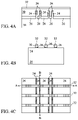
- FIGS. 4A, 4B, 4C and 4D illustrate the formation of dummy gate stacks on the fins 24 .
- FIGS. 4A and 4B illustrate cross-sectional views;
- FIG. 4C illustrates a top view; and
- FIG. 4D illustrates a three-dimensional view.
- FIGS. 4C and 4D illustrate cross-sections A-A and B-B.
- FIGS. 1, 2, 3A, 4A , and the following figures ending with an “A” designation illustrate cross-sectional views at various instances of processing corresponding to cross-section A-A
- FIGS. 4B and the following figures ending with a “B” designation illustrate cross-sectional views at various instances of processing corresponding to cross-section B-B.
- some reference numbers of components or features illustrated therein may be omitted to avoid obscuring other components or features; this is for ease of depicting the figures.
- the dummy gate stacks are over and extend laterally perpendicularly to the fins 24 .
- Each dummy gate stack comprises one or more interfacial dielectrics 28 , a dummy gate 30 , and a mask 32 .
- the one or more interfacial dielectrics 28 , dummy gates 30 , and mask 32 for the dummy gate stacks may be formed by sequentially forming respective layers, and then patterning those layers into the dummy gate stacks.
- a layer for the one or more interfacial dielectrics 28 may include or be silicon oxide, silicon nitride, the like, or multilayers thereof, and may be thermally and/or chemically grown on the fins 24 , as illustrated, or conformally deposited, such as by plasma-enhanced CVD (PECVD), ALD, or another deposition technique.
- PECVD plasma-enhanced CVD
- a layer for the dummy gates 30 may include or be silicon (e.g., polysilicon) or another material deposited by CVD, PVD, or another deposition technique.
- a layer for the mask 32 may include or be silicon nitride, silicon oxynitride, silicon carbon nitride, the like, or a combination thereof, deposited by CVD, PVD, ALD, or another deposition technique.
- the layers for the mask 32 , dummy gates 30 , and one or more interfacial dielectrics 28 may then be patterned, for example, using photolithography and one or more etch processes, like described above, to form the mask 32 , dummy gate 30 , and one or more interfacial dielectrics 28 for each dummy gate stack.
- a dummy gate stack is implemented for a replacement gate process.
- a gate-first process may be implemented using gate stacks including, for example, a gate dielectric in the place of the one or more interfacial dielectrics 28 , and a gate electrode in the place of the dummy gate 30 .
- the gate stacks may be formed using similar processes and materials as described with respect to the dummy gate stacks; although in other examples, other processes or materials may be implemented.
- a gate dielectric may include or be a high-k dielectric material, such as having a k value greater than about 7.0, which may include a metal oxide or silicate of Hf, Al, Zr, La, Mg, Ba, Ti, Pb, multilayers thereof, or a combination thereof.
- a gate dielectric may also be deposited by molecular-beam deposition (MBD), ALD, PECVD, or another deposition technique.
- a gate electrode may also include or be a metal-containing material such as TiN, TaN, TaC, Co, Ru, Al, multi-layers thereof, or a combination thereof, and may also be deposited by CVD, PVD, or another deposition technique.
- the cross-section A-A is along a dummy gate stack through which a gate cut and a fin cut will be made in subsequent figures and description.
- the cross-section B-B is along a fin 24 (e.g., along a channel direction in the fin 24 ) through which a fin cut will be made in subsequent figures and description.
- Cross-sections A-A and B-B are perpendicular to each other.
- FIGS. 5A, 5B, and 5C illustrate the formation of gate spacers 34 .
- Gate spacers 34 are formed along sidewalls of the dummy gate stacks (e.g., sidewalls of the one or more interfacial dielectrics 28 , dummy gate 30 , and mask 32 ) and over the fins 24 . Residual gate spacers 34 may also be formed along sidewalls of the fins 24 .
- the gate spacers 34 may be formed by conformally depositing one or more layers for the gate spacers 34 and anisotropically etching the one or more layers, for example.
- the one or more layers for the gate spacers 34 may include or be silicon carbon oxide, silicon nitride, silicon oxynitride, silicon carbon nitride, the like, multi-layers thereof, or a combination thereof, and may be deposited by CVD, ALD, or another deposition technique.
- the etch process can include a RIE, NBE, or another etch process.
- Source/drain regions 35 are formed in the fins 24 .
- the source/drain regions 35 are formed by implanting dopants into the fins 24 using the dummy gate stacks and gate spacers 34 as masks.
- source/drain regions 35 can be formed by implantation on opposing sides of each dummy gate stack.
- the fins 24 may be recessed using the dummy gate stacks and gate spacers 34 as masks, and epitaxial source/drain regions 35 may be epitaxially grown in the recesses. Epitaxial source/drain regions 35 may be raised in relation to the fin 24 , as illustrated by dashed lines in FIG. 5B .
- the epitaxial source/drain regions 35 may be doped by in situ doping during the epitaxial growth and/or by implantation after the epitaxial growth. Hence, source/drain regions 35 can be formed by epitaxial growth, and possibly with implantation, on opposing sides of each dummy gate stack.
- Example dopants for source/drain regions 35 can include or be, for example, boron for a p-type device and phosphorus or arsenic for an n-type device, although other dopants may be used.
- the source/drain regions 35 may have a dopant concentration in a range from about 10 19 cm ⁇ 3 to about 10 21 cm ⁇ 3 .
- the source/drain regions 35 are not expressly illustrated in subsequent figures to avoid obscuring other features and components depicted in those figures; however, a person having ordinary skill in the art will readily understand that the source/drain regions 35 are present in the structures depicted in those figures.
- FIGS. 6A, 6B, and 6C illustrate the formation of one or more dielectric layers 36 .
- the one or more dielectric layers 36 may include an etch stop layer (ESL) and an interlayer dielectric (ILD), for example.
- ESL etch stop layer
- ILD interlayer dielectric
- an etch stop layer can provide a mechanism to stop an etch process when forming, e.g., contacts or vias.
- An etch stop layer may be formed of a dielectric material having a different etch selectivity from adjacent layers, for example, the interlayer dielectric.
- the etch stop layer may be conformally deposited over the fins 24 , dummy gate stacks, gate spacers 34 , and isolation regions 26 .
- the etch stop layer may comprise or be silicon nitride, silicon carbon nitride, silicon carbon oxide, carbon nitride, the like, or a combination thereof, and may be deposited by CVD, PECVD, ALD, or another deposition technique.
- the interlayer dielectric may comprise or be silicon dioxide, a low-k dielectric material (e.g., a material having a dielectric constant lower than silicon dioxide), such as silicon oxynitride, phosphosilicate glass (PSG), borosilicate glass (BSG), borophosphosilicate glass (BPSG), undoped silicate glass (USG), fluorinated silicate glass (FSG), organosilicate glasses (OS G), SiO x C y , Spin-On-Glass, Spin-On-Polymers, silicon carbon material, a compound thereof, a composite thereof, the like, or a combination thereof.
- the interlayer dielectric may be deposited by spin-on, CVD, FCVD, PECVD, PVD, or another deposition technique.
- the one or more dielectric layers 36 are formed with top surface(s) coplanar with top surfaces of the dummy gates 30 .
- a planarization process such as a CMP, may be performed to level the top surface of the one or more dielectric layers 36 with the top surfaces of the dummy gates 30 .
- the CMP may also remove the mask 32 (and, in some instances, upper portions of the gate spacers 34 ) on the dummy gates 30 . Accordingly, top surfaces of the dummy gates 30 are exposed through the one or more dielectric layers 36 .
- FIGS. 7A, 7B, and 7C illustrate forming cut openings 42 to cut dummy gate stacks.
- a mask 40 e.g., a hard mask
- one or more mask layers are deposited over the dummy gate stacks, the gate spacers 34 , and the one or more dielectric layers 36 , and the one or more mask layers are then patterned to form the mask 40 with mask openings corresponding to the cut openings 42 .
- the one or more mask layers may include or be silicon nitride, silicon oxynitride, silicon carbide, silicon carbon nitride, the like, or a combination thereof, and may be deposited by CVD, PVD, ALD, or another deposition technique.
- the one or more mask layers may be patterned using photolithography and etch processes, as previously described.
- the mask 40 can have mask openings (each corresponding to a cut opening 42 ) extending in a direction laterally perpendicular to and intersecting the dummy gate stacks that are to be cut.
- the dummy gate stacks, gate spacers 34 , and one or more dielectric layers 36 may be etched such that cut openings 42 are formed cutting the dummy gate stacks.
- the cut openings 42 can extend to a depth to and/or into the corresponding isolation regions 26 , e.g., through the dummy gates 30 and, depending on the implementation, the one or more interfacial dielectrics 28 .
- the etch process may include a RIE, NBE, ICP etch, the like, or a combination thereof.
- the etching may be anisotropic.
- FIGS. 8A, 8B, and 8C illustrate forming gate cut-fill structures 44 in the cut openings 42 .
- An insulating material for the gate cut-fill structures 44 is deposited in the cut openings 42 that cut the dummy gate stacks.
- the gate cut-fill structures 44 can extend to and/or into the corresponding isolation regions 26 (e.g., a bottom surface of the gate cut-fill structure 44 can be at a depth below a top surface of the corresponding isolation region 26 ).
- each of the gate cut-fill structures 44 may be a single insulating material, and in other examples, the gate cut-fill structures 44 may include multiple different insulating materials, such as in a multi-layered configuration.
- the insulating material may include or be silicon oxide, silicon nitride, silicon oxynitride, silicon carbide, silicon carbon nitride, the like, or a combination thereof, and may be deposited by CVD, PVD, ALD, or another deposition technique. Portions of the insulating material for the gate cut-fill structures 44 and the mask 40 above the top surface of the one or more dielectric layers 36 are removed.
- a planarization process may remove the portions of the insulating material for the gate cut-fill structures 44 and the mask 40 above the top surface of the one or more dielectric layers 36 , and top surfaces of the gate cut-fill structures 44 may be formed coplanar with the top surface of the one or more dielectric layers 36 .
- the gate cut-fill structures 44 therefore electrically isolate sections of the dummy gate stacks that were cut from each other.
- FIGS. 9A, 9B, and 9C illustrate the formation of cut openings 52 to cut fins 24 .
- a mask 50 e.g., a hard mask
- one or more mask layers are deposited over the dummy gate stacks, the gate spacers 34 , the one or more dielectric layers 36 , and the gate cut-fill structures 44 , and the one or more mask layers are then patterned to form the mask 50 with mask openings corresponding to the cut openings 52 .
- the one or more mask layers may include or be silicon nitride, silicon oxynitride, silicon carbide, silicon carbon nitride, the like, or a combination thereof, and may be deposited by CVD, PVD, ALD, or another deposition technique.
- the one or more mask layers may be patterned using photolithography and etch processes, as previously described.
- the mask 50 can have mask openings (each corresponding to a cut opening 52 ) extending in a direction laterally perpendicular to and intersecting the fins 24 that are to be cut.
- the dummy gate stacks, gate cut-fill structures 44 , and fins 24 exposed by the cut openings 52 in the mask 50 are etched such that cut openings 52 are formed cutting the exposed fins 24 .
- the cut openings 52 can extend to a depth below upper surfaces of the isolation regions 26 .
- the etching can form the cut openings 52 extending into the isolation regions 26 where fins 24 were cut.
- Fin cut regions 54 where the fins 24 were cut remain on the semiconductor substrate 20 .
- the fin cut regions 54 are between neighboring isolation regions 26 and have top surfaces below the top surfaces of the neighboring isolation regions 26 .
- the etch process may include a RIE, NBE, ICP etch, the like, or a combination thereof.
- the etching may be anisotropic.
- the mask 50 may be removed after the cut openings 52 cutting the fins 24 have been formed.
- FIGS. 10A, 10B, and 10C illustrate the formation of an insulating liner 56 conformally in the cut openings 52 where the fins 24 were cut and a fill material 58 on the insulating liner 56 .
- the insulating liner 56 may include or be a high band gap material, such as a material having a band gap that is equal to or greater than about 5 eV, which may also be equal to or greater than about twice the band gap of silicon nitride.
- Example high band gap materials include silicon oxide (SiO x ), aluminum oxide (Al 2 O 3 ), titanium oxide (TiO x ), tantalum oxide (TaO x ), aluminum fluoride (AlF), aluminum oxyfluoride (AlOF x ), zirconium silicate (ZrSiO x ), hafnium silicate (HfSiO x ), hafnium oxide (HfO 2 ), zirconium oxide (ZrO 2 ), or a combination thereof.
- Some examples use an ALD process to form the insulating liner 56 .
- Such an ALD process may use one or more precursors such as SiH 2 [N(C 2 H 5 ) 2 ] 2 , silane (SiH 4 ), oxygen (O 2 ), trimethylaluminum (Al 2 (CH 3 ) 6 ), steam (H 2 O), ozone (O 3 ), fluorine (F 2 ), and nitrogen trifluoride (NF 3 ) to deposit the example high band gap materials listed above or other materials, and may use a radio frequency (RF) power in a range from about 100 W to about 1,000 W, a pressure in a range from about 2 torr to about 9 torr, and a temperature in a range from about 45° C. to about 700° C.
- RF radio frequency
- the fill material 58 may be an insulating material. In some examples, fill material 58 may be a single insulating material, and in other examples, fill material 58 may include multiple different insulating materials, such as in a multi-layered configuration.
- the fill material 58 may include or be silicon nitride, silicon oxynitride, silicon carbide, silicon carbon nitride, the like, or a combination thereof, and may be deposited by ALD, thermal deposition, CVD, or another deposition technique. In an example, the fill material 58 is silicon nitride deposited by ALD or CVD.
- FIGS. 11A, 11B, and 11C illustrate the removal of excess portions of the fill material 58 and the insulating liner 56 above the top surface of the one or more dielectric layers 36 , gate spacers 34 , gate cut-fill structures 44 , and dummy gate stacks to form fin cut-fill structures.
- a planarization process like a CMP, may remove the portions of the fill material 58 and the insulating liner 56 above the top surface of the one or more dielectric layers 36 , etc., and top surfaces of the fin cut-fill structures may be formed coplanar with the top surface of the one or more dielectric layers 36 , etc.
- the planarization process may further expose the dummy gates 30 for subsequent replacement of the dummy gate stacks.
- Each fin cut-fill structure includes the fill material 58 and the insulating liner 56 .
- the cutting of the fins 24 forms fin cut-fill structures that extend laterally perpendicularly to and dissect the fins 24 that are cut. Sections of a fin 24 that were integral before the cutting of the fin 24 can be made to be electrically isolated sections from each other because of the fin cut-fill structure.
- FIGS. 12A, 12B, and 12C illustrate the replacement of the dummy gate stacks with replacement gate structures.
- the processing of FIGS. 12A, 12B, and 12C may be omitted.
- the dummy gates 30 and one or more interfacial dielectrics 28 are removed, such as by one or more etch processes.
- the dummy gates 30 may be removed by an etch process selective to the dummy gates 30 , wherein the one or more interfacial dielectrics 28 act as etch stop layers, and subsequently, the one or more interfacial dielectrics 28 can be removed by a different etch process selective to the one or more interfacial dielectrics 28 .
- the etch processes can be, for example, a RIE, NBE, a wet etch, or another etch process.
- Recesses are formed between gate spacers 34 where the dummy gate stacks are removed, and channel regions of the fins 24 are exposed through the recesses.
- the replacement gate structures are formed in the recesses formed where the dummy gate stacks were removed.
- the replacement gate structures each include one or more conformal layers 60 and a gate electrode 62 .
- the one or more conformal layers 60 include a gate dielectric layer and may include one or more work-function tuning layers.
- the gate dielectric layer can be conformally deposited in the recesses where dummy gate stacks were removed (e.g., on top surfaces of the isolation regions 26 , sidewalls and top surfaces of the fins 24 along the channel regions, and sidewalls of the gate spacers 34 and gate cut-fill structures 44 ) and on the top surfaces of the one or more dielectric layers 36 , gate spacers 34 , and gate cut-fill structures 44 .
- the gate dielectric layer can be or include silicon oxide, silicon nitride, a high-k dielectric material, multilayers thereof, or other dielectric material.
- a high-k dielectric material may have a k value greater than about 7.0, and may include a metal oxide of or a metal silicate of Hf, Al, Zr, La, Mg, Ba, Ti, Pb, or a combination thereof.
- the gate dielectric layer can be deposited by ALD, PECVD, MBD, or another deposition technique.
- a work-function tuning layer may be conformally deposited on the gate dielectric layer.
- the work-function tuning layer may include or be tantalum, tantalum nitride, titanium, titanium nitride, the like, or a combination thereof, and may be deposited by ALD, PECVD, MBD, or another deposition technique. Any additional work-function tuning layers may be sequentially deposited similar to the first work-function tuning layer.
- a layer for the gate electrodes 62 is formed over the one or more conformal layers 60 .
- the layer for the gate electrodes 62 can fill remaining recesses where the dummy gate stacks were removed.
- the layer for the gate electrodes 62 may be or comprise a metal-containing material such as Co, Ru, Al, W, Cu, multi-layers thereof, or a combination thereof.
- the layer for the gate electrodes 62 can be deposited by ALD, PECVD, MBD, PVD, or another deposition technique.
- Portions of the layer for the gate electrodes 62 and of the one or more conformal layers 60 above the top surfaces of the one or more dielectric layers 36 , gate spacers 34 , and gate cut-fill structures 44 are removed.
- a planarization process like a CMP, may remove the portions of the layer for the gate electrodes 62 and the one or more conformal layers 60 above the top surfaces of the one or more dielectric layers 36 , gate spacers 34 , and gate cut-fill structures 44 .
- the replacement gate structures comprising the gate electrodes 62 and one or more conformal layers 60 may therefore be formed as illustrated in FIGS. 12A-C .
- FIGS. 13A, 13B, and 13C illustrate the formation of one or more dielectric layers 70 and conductive features 72 in the one or more dielectric layers 36 and/or 70 to source/drain regions 35 of the fins 24 and to gate electrodes 62 .
- the one or more dielectric layers 70 may include an etch stop layer (ESL) and an interlayer dielectric (ILD) or intermetal dielectric (IMD), for example.
- the etch stop layer may be deposited over the one or more dielectric layers 36 , gate cut-fill structures 44 , fin cut-fill structures, gate spacers 34 , gate electrodes 62 , and one or more conformal layers 60 .
- the etch stop layer may comprise or be silicon nitride, silicon carbon nitride, silicon carbon oxide, carbon nitride, the like, or a combination thereof, and may be deposited by CVD, PECVD, ALD, or another deposition technique.
- the interlayer dielectric or intermetal dielectric may comprise or be silicon dioxide, a low-k dielectric material, such as silicon oxynitride, PSG, BSG, BPSG, USG, FSG, OSG, SiO x C y , Spin-On-Glass, Spin-On-Polymers, silicon carbon material, a compound thereof, a composite thereof, the like, or a combination thereof.
- the interlayer dielectric or intermetal dielectric may be deposited by spin-on, CVD, FCVD, PECVD, PVD, or another deposition technique.
- Recesses and/or openings can be formed in and/or through the dielectric layers 70 and 36 to the source/drain regions 35 and gate electrodes 62 to expose at least portions of the source/drain regions 35 and gate electrodes 62 , respectively.
- the dielectric layers 70 and 36 may be patterned with the recesses and/or openings, for example, using photolithography and one or more etch processes.
- the conductive features 72 may then be formed in the recesses and/or openings.
- the conductive features 72 may include an adhesion and/or barrier layer and conductive material on the adhesion and/or barrier layer, for example. In some examples, the conductive features 72 may include silicide regions.
- the adhesion and/or barrier layer can be conformally deposited in the recesses and/or openings and over the one or more dielectric layers 70 .
- the adhesion and/or barrier layer may be or comprise titanium, titanium nitride, titanium oxide, tantalum, tantalum nitride, tantalum oxide, the like, or a combination thereof, and may be deposited by ALD, CVD, or another deposition technique.
- Silicide regions may be formed on upper portions of the source/drain regions 35 by reacting upper portions of the source/drain regions 35 with the adhesion and/or barrier layer. An anneal can be performed to facilitate the reaction of the source/drain regions 35 with the adhesion and/or barrier layer.
- the conductive material can be deposited on the adhesion and/or barrier layer and fill the recesses and/or openings.
- the conductive material may be or comprise tungsten, copper, aluminum, gold, silver, alloys thereof, the like, or a combination thereof, and may be deposited by CVD, ALD, PVD, or another deposition technique.
- CVD chemical vapor deposition
- ALD atomic layer deposition
- PVD physical vapor deposition
- excess material may be removed by using a planarization process, such as a CMP, for example.
- the planarization process may remove excess material of the conductive features 72 from above a top surface of the one or more dielectric layers 70 .
- top surfaces of the conductive features 72 and the one or more dielectric layers 70 may be coplanar.
- the conductive features 72 may be or may be referred to as contacts, plugs, etc.
- the conductive features 72 are formed to the source/drain regions 35 of the fins 24 or to replacement gate structures to electrically couple the source/drain regions 35 or the replacement gate structures, respectively.
- the layout of the conductive features 72 in the figures is merely an example. A person having ordinary skill in the art will readily understand that a layout of conductive features can differ between different implementations.
- FIG. 14 illustrates a cross-sectional view of an example fin cut-fill structure in accordance with some embodiments.
- the fin cut-fill structure includes the insulating liner 56 and the fill material 58 as described with respect to and illustrated in previous figures.
- the fin cut-fill structure in the illustrated cross-section is disposed laterally between gate spacers 34 and extends vertically to a depth below a level of an upper surface of a neighboring isolation region 26 (shown in phantom). Laterally, the insulating liner 56 is disposed between a respective gate spacer 34 and the fill material 58 , and between a respective section of the cut fin 24 and the fill material 58 .
- the insulating liner 56 is disposed between (i) the semiconductor substrate 20 and/or remaining portion of a cut region of the fin 24 and (ii) the fill material 58 .
- the insulating liner 56 is disposed between the isolation region 26 (as shown in phantom) and the fill material 58 .
- the insulating liner 56 is conformally disposed between the fill material 58 and other structures formed on and/or from the semiconductor substrate 20 .
- the fin cut-fill structure has a vertical dimension D 1 , which extends from a top surface of the fin cut-fill structure to a depth below a level of an upper surface of a neighboring isolation region 26 (as shown in phantom).
- the fin cut-fill structure has a lateral dimension D 2 at the top surface of the fin cut-fill structure.
- the vertical dimension D 1 is in a range from about 200 nm to about 320 nm
- the lateral dimension D 2 is in a range from about 20 nm to about 25 nm.
- An aspect ratio of the vertical dimension D 1 to the lateral dimension D 2 in some examples, is greater than or equal to about 10, such as about 13.
- the depth D 3 that the fin 24 is cut is in a range from about 130 nm to about 190 nm.
- a height D 4 of the fin 24 is in a range from about 40 nm to about 70 nm.
- a height D 5 of the one or more dielectric layers 36 from a top surface of a fin 24 is in a range from about 70 nm to about 130 nm.
- a thickness D 6 of the insulating liner 56 at an upper portion of the fin cut-fill structure is in a range from about 2 nm to about 6 nm
- a thickness D 7 of the insulating liner 56 at a lower portion of the fin cut-fill structure is in a range from about 1.6 nm to about 6 nm
- a ratio of the thickness D 7 at the lower portion to the thickness D 6 at the upper portion is in a range from about 1.0 to about 0.8.
- Some embodiments may achieve advantages.
- a high band gap material as an insulating liner in a fin cut-fill structure
- leakage between neighboring sections of a fin that was cut e.g., sections of a fin that the fin cut-fill structure is between and abuts
- WAT wafer acceptance testing
- An embodiment is a structure.
- the structure includes a first fin on a substrate, a second fin on the substrate, and a fin cut-fill structure disposed between the first fin and the second fin.
- the first fin and the second fin are longitudinally aligned.
- the fin cut-fill structure includes an insulating liner and a fill material on the insulating liner.
- the insulating liner abuts a first sidewall of the first fin and a second sidewall of the second fin.
- the insulating liner includes a material with a band gap greater than 5 eV.
- the structure includes an insulator structure disposed laterally between a first fin and a second fin.
- the first fin and the second fin are longitudinally aligned on a substrate.
- the insulator structure includes a high band gap liner disposed along respective end sidewalls of the first fin and the second fin, and includes a fill material on the high band gap liner.
- the high band gap liner has a band gap greater than 5 eV.
- a further embodiment is a method.
- a fin is formed on a substrate.
- the fin is cut into a first section of the fin and a second section of the fin by forming a cut opening between the first section of the fin and the second section of the fin.
- a conformal liner layer is formed in the cut opening.
- the conformal liner layer includes a material with a band gap greater than 5 eV.
- a fill material is formed on the conformal liner layer in the cut opening.
Abstract
Description
Claims (20)
Priority Applications (2)
| Application Number | Priority Date | Filing Date | Title |
|---|---|---|---|
| US17/019,475 US11380593B2 (en) | 2017-11-28 | 2020-09-14 | Semiconductor fin cutting process and structures formed thereby |
| US17/852,716 US20220328360A1 (en) | 2017-11-28 | 2022-06-29 | Semiconductor Fin Cutting Process and Structures Formed Thereby |
Applications Claiming Priority (3)
| Application Number | Priority Date | Filing Date | Title |
|---|---|---|---|
| US201762591647P | 2017-11-28 | 2017-11-28 | |
| US15/922,656 US10777466B2 (en) | 2017-11-28 | 2018-03-15 | Semiconductor Fin cutting process and structures formed thereby |
| US17/019,475 US11380593B2 (en) | 2017-11-28 | 2020-09-14 | Semiconductor fin cutting process and structures formed thereby |
Related Parent Applications (1)
| Application Number | Title | Priority Date | Filing Date |
|---|---|---|---|
| US15/922,656 Continuation US10777466B2 (en) | 2017-11-28 | 2018-03-15 | Semiconductor Fin cutting process and structures formed thereby |
Related Child Applications (1)
| Application Number | Title | Priority Date | Filing Date |
|---|---|---|---|
| US17/852,716 Continuation US20220328360A1 (en) | 2017-11-28 | 2022-06-29 | Semiconductor Fin Cutting Process and Structures Formed Thereby |
Publications (2)
| Publication Number | Publication Date |
|---|---|
| US20200411386A1 US20200411386A1 (en) | 2020-12-31 |
| US11380593B2 true US11380593B2 (en) | 2022-07-05 |
Family
ID=66442140
Family Applications (3)
| Application Number | Title | Priority Date | Filing Date |
|---|---|---|---|
| US15/922,656 Active US10777466B2 (en) | 2017-11-28 | 2018-03-15 | Semiconductor Fin cutting process and structures formed thereby |
| US17/019,475 Active US11380593B2 (en) | 2017-11-28 | 2020-09-14 | Semiconductor fin cutting process and structures formed thereby |
| US17/852,716 Pending US20220328360A1 (en) | 2017-11-28 | 2022-06-29 | Semiconductor Fin Cutting Process and Structures Formed Thereby |
Family Applications Before (1)
| Application Number | Title | Priority Date | Filing Date |
|---|---|---|---|
| US15/922,656 Active US10777466B2 (en) | 2017-11-28 | 2018-03-15 | Semiconductor Fin cutting process and structures formed thereby |
Family Applications After (1)
| Application Number | Title | Priority Date | Filing Date |
|---|---|---|---|
| US17/852,716 Pending US20220328360A1 (en) | 2017-11-28 | 2022-06-29 | Semiconductor Fin Cutting Process and Structures Formed Thereby |
Country Status (5)
| Country | Link |
|---|---|
| US (3) | US10777466B2 (en) |
| KR (1) | KR102209949B1 (en) |
| CN (1) | CN109841619B (en) |
| DE (1) | DE102018106631A1 (en) |
| TW (1) | TWI671903B (en) |
Families Citing this family (12)
| Publication number | Priority date | Publication date | Assignee | Title |
|---|---|---|---|---|
| US10811320B2 (en) * | 2017-09-29 | 2020-10-20 | Taiwan Semiconductor Manufacturing Company, Ltd. | Footing removal in cut-metal process |
| US11114549B2 (en) * | 2017-11-29 | 2021-09-07 | Taiwan Semiconductor Manufacturing Co., Ltd. | Semiconductor structure cutting process and structures formed thereby |
| US20210125875A1 (en) * | 2019-10-29 | 2021-04-29 | Taiwan Semiconductor Manufacturing Co., Ltd. | Semiconductor device and method |
| US11545490B2 (en) * | 2019-12-17 | 2023-01-03 | Taiwan Semiconductor Manufacturing Co., Ltd. | Semiconductor structure and method for forming the same |
| US11404323B2 (en) | 2020-04-29 | 2022-08-02 | Taiwan Semiconductor Manufacturing Co., Ltd. | Formation of hybrid isolation regions through recess and re-deposition |
| DE102020119859A1 (en) | 2020-04-29 | 2021-11-04 | Taiwan Semiconductor Manufacturing Co., Ltd. | FORMATION OF HYBRID ISOLATION REGIONS THROUGH RECESSING AND RE-SEPARATION |
| US11348917B2 (en) * | 2020-04-30 | 2022-05-31 | Taiwan Semiconductor Manufacturing Co., Ltd. | Semiconductor device with isolation structure |
| US11302581B2 (en) * | 2020-05-05 | 2022-04-12 | Taiwan Semiconductor Manufacturing Company, Ltd. | Gate profile control through sidewall protection during etching |
| US11335603B2 (en) * | 2020-06-26 | 2022-05-17 | Taiwan Semiconductor Manufacturing Company, Ltd. | Multi-layered insulating film stack |
| US11862508B2 (en) * | 2020-08-12 | 2024-01-02 | Taiwan Semiconductor Manufacturing Co., Ltd. | FinFET device and method of forming same |
| US11532744B2 (en) | 2020-10-26 | 2022-12-20 | Taiwan Semiconductor Manufacturing Company, Ltd. | Gate cut structure and method of forming the same |
| KR20220145195A (en) | 2021-04-21 | 2022-10-28 | 삼성전자주식회사 | Semiconductor devices and methods of manufacturing the same |
Citations (46)
| Publication number | Priority date | Publication date | Assignee | Title |
|---|---|---|---|---|
| US20070134884A1 (en) | 2005-12-14 | 2007-06-14 | Samsung Electronics Co., Ltd. | Isolation method of defining active fins, method of fabricating semiconductor device using the same and semiconductor device fabricated thereby |
| US20080230373A1 (en) | 2007-03-21 | 2008-09-25 | Samsung Electronics Co., Ltd. | Methods of forming a phase-change material layer including tellurium and methods of manufacturing a phase-change memory device using the same |
| US20080305561A1 (en) | 2007-06-07 | 2008-12-11 | Shrinivas Govindarajan | Methods of controlling film deposition using atomic layer deposition |
| US20140038387A1 (en) | 2010-01-29 | 2014-02-06 | Elpida Memory, Inc. | Method for manufacturing a semiconductor device |
| US20140227857A1 (en) | 2013-02-08 | 2014-08-14 | Samsung Electronics Co., Ltd. | Methods of Fabricating Semiconductor Devices Including Fin-Shaped Active Regions |
| US20140374828A1 (en) | 2013-06-21 | 2014-12-25 | Tae-Joong Song | Semiconductor device and method for fabricating the same |
| US8987836B2 (en) | 2012-04-23 | 2015-03-24 | Samsung Electronics Co., Ltd. | Field effect transistor having fin base and at lease one fin protruding from fin base |
| US9006067B2 (en) | 2013-02-14 | 2015-04-14 | Samsung Electronics Co., Ltd. | Semiconductor device and method of fabricationg the same |
| US20150104923A1 (en) | 2013-10-04 | 2015-04-16 | Taiwan Semiconductor Manufacturing Company, Ltd. | Mechanism of Forming a Trench Structure |
| US20150111362A1 (en) | 2013-10-18 | 2015-04-23 | Taiwan Semiconductor Manufacturing Company, Ltd. | Method Of Making A FinFET Device |
| US9105490B2 (en) | 2012-09-27 | 2015-08-11 | Taiwan Semiconductor Manufacturing Company, Ltd. | Contact structure of semiconductor device |
| US20150228796A1 (en) | 2004-02-05 | 2015-08-13 | Samsung Electronics Co., Ltd. | Fin fet and method of fabricating same |
| US20160005738A1 (en) | 2014-07-07 | 2016-01-07 | Samsung Electronics Co., Ltd. | Semiconductor device having a fin structure and method of manufacture the same |
| US9236300B2 (en) | 2012-11-30 | 2016-01-12 | Taiwan Semiconductor Manufacturing Company, Ltd. | Contact plugs in SRAM cells and the method of forming the same |
| US9236267B2 (en) | 2012-02-09 | 2016-01-12 | Taiwan Semiconductor Manufacturing Company, Ltd. | Cut-mask patterning process for fin-like field effect transistor (FinFET) device |
| US20160056045A1 (en) | 2014-08-22 | 2016-02-25 | United Microelectronics Corp. | Fin structure and method of forming the same |
| US20160071857A1 (en) | 2014-09-05 | 2016-03-10 | Kabushiki Kaisha Toshiba | Manufacturing method of semiconductor memory device |
| KR20160032939A (en) | 2014-09-17 | 2016-03-25 | 삼성전자주식회사 | Integrated circuit device and method of manufacturing the same |
| KR20160056693A (en) | 2014-11-12 | 2016-05-20 | 삼성전자주식회사 | Integrated circuit device and method of manufacturing the same |
| US9406804B2 (en) | 2014-04-11 | 2016-08-02 | Taiwan Semiconductor Manufacturing Company, Ltd. | FinFETs with contact-all-around |
| US9443769B2 (en) | 2014-04-21 | 2016-09-13 | Taiwan Semiconductor Manufacturing Company, Ltd. | Wrap-around contact |
| US20160329249A1 (en) | 2012-10-15 | 2016-11-10 | Marvell World Trade Ltd. | Isolation components for transistors formed on fin features of semiconductor substrates |
| US20160351590A1 (en) | 2015-05-27 | 2016-12-01 | International Business Machines Corporation | Preventing strained fin relaxation |
| US9520482B1 (en) | 2015-11-13 | 2016-12-13 | Taiwan Semiconductor Manufacturing Company, Ltd. | Method of cutting metal gate |
| US20160380075A1 (en) | 2015-06-24 | 2016-12-29 | Samsung Electronics Co., Ltd. | Semiconductor device |
| US9548366B1 (en) | 2016-04-04 | 2017-01-17 | Taiwan Semiconductor Manufacturing Company, Ltd. | Self aligned contact scheme |
| US9576814B2 (en) | 2013-12-19 | 2017-02-21 | Taiwan Semiconductor Manufacturing Company, Ltd. | Method of spacer patterning to form a target integrated circuit pattern |
| US20170062584A1 (en) | 2015-09-02 | 2017-03-02 | International Business Machines Corporation | Composite spacer enabling uniform doping in recessed fin devices |
| US20170092643A1 (en) | 2015-09-25 | 2017-03-30 | United Microelectronics Corp. | Semiconductor device and method of fabricating the same |
| US20170103985A1 (en) | 2015-10-07 | 2017-04-13 | Ki-Il KIM | Integrated circuit device and method of manufacturing the same |
| KR20170051120A (en) | 2015-11-02 | 2017-05-11 | 타이완 세미콘덕터 매뉴팩쳐링 컴퍼니 리미티드 | Structure and formation method of semiconductor device structure |
| US20170170182A1 (en) | 2015-12-09 | 2017-06-15 | International Business Machines Corporation | Tall strained high percentage silicon germanium fins for cmos |
| US9704751B1 (en) | 2016-02-26 | 2017-07-11 | Taiwan Semiconductor Manufacturing Co., Ltd. | Semiconductor device and method for fabricating the same |
| US20170207097A1 (en) | 2015-03-16 | 2017-07-20 | International Business Machines Corporation | Method to improve finfet cut overlay |
| US20170213823A1 (en) | 2016-01-26 | 2017-07-27 | Ji-Hoon Cha | Semiconductor device and a fabricating method thereof |
| US20170330957A1 (en) | 2016-05-11 | 2017-11-16 | International Business Machines Corporation | Fabrication Of Vertical Field Effect Transistor Structure With Strained Channels |
| US9831183B2 (en) | 2014-08-07 | 2017-11-28 | Taiwan Semiconductor Manufacturing Company, Ltd. | Contact structure and method of forming |
| US20180138174A1 (en) * | 2016-11-14 | 2018-05-17 | Samsung Electronics Co., Ltd. | Semiconductor device and method for fabricating the same |
| US20180138269A1 (en) | 2016-11-16 | 2018-05-17 | Samsung Electronics Co., Ltd. | Semiconductor device and method for fabricating the same |
| US20180211887A1 (en) | 2016-01-21 | 2018-07-26 | Samsung Electronics Co., Ltd. | Semiconductor device |
| US20180211866A1 (en) | 2017-01-25 | 2018-07-26 | International Business Machines Corporation | Forming sacrificial endpoint layer for deep sti recess |
| US20180350585A1 (en) | 2017-05-31 | 2018-12-06 | Taiwan Semiconductor Manufacturing Co., Ltd. | Method and Structure for FinFET Devices |
| US20190006345A1 (en) | 2017-06-29 | 2019-01-03 | Taiwan Semiconductor Manufacturing Co., Ltd. | Metal gate structure cutting process |
| US20190067111A1 (en) | 2017-08-31 | 2019-02-28 | Taiwan Semiconductor Manufacturing Co., Ltd. | Fin field effect transistor (finfet) device structure with dummy fin structure and method for forming the same |
| US10283415B2 (en) | 2017-06-08 | 2019-05-07 | United Microelectronics Corp. | Semiconductor structure with a bump having a width larger than a width of fin shaped structures and manufacturing method thereof |
| US20190172950A1 (en) | 2016-09-30 | 2019-06-06 | Intel Corporation | Finfet transistor with channel stress induced via stressor material inserted into fin plug region enabled by backside reveal |
Family Cites Families (5)
| Publication number | Priority date | Publication date | Assignee | Title |
|---|---|---|---|---|
| TWI648857B (en) * | 2015-05-07 | 2019-01-21 | 聯華電子股份有限公司 | Semiconductor device and method for fabricating the same |
| CN106711213B (en) * | 2015-07-20 | 2021-02-26 | 联华电子股份有限公司 | Semiconductor element and manufacturing method thereof |
| US10340348B2 (en) * | 2015-11-30 | 2019-07-02 | Taiwan Semiconductor Manufacturing Co., Ltd. | Method of manufacturing finFETs with self-align contacts |
| US10163898B2 (en) * | 2016-04-25 | 2018-12-25 | Taiwan Semiconductor Manufacturing Company, Ltd. | FinFETs and methods of forming FinFETs |
| TWI691076B (en) * | 2016-08-03 | 2020-04-11 | 聯華電子股份有限公司 | Semiconductor structure and method of forming the same |
-
2018
- 2018-03-15 US US15/922,656 patent/US10777466B2/en active Active
- 2018-03-21 DE DE102018106631.7A patent/DE102018106631A1/en active Pending
- 2018-06-07 KR KR1020180065574A patent/KR102209949B1/en active IP Right Grant
- 2018-08-14 CN CN201810920097.6A patent/CN109841619B/en active Active
- 2018-08-20 TW TW107128972A patent/TWI671903B/en active
-
2020
- 2020-09-14 US US17/019,475 patent/US11380593B2/en active Active
-
2022
- 2022-06-29 US US17/852,716 patent/US20220328360A1/en active Pending
Patent Citations (50)
| Publication number | Priority date | Publication date | Assignee | Title |
|---|---|---|---|---|
| US20150228796A1 (en) | 2004-02-05 | 2015-08-13 | Samsung Electronics Co., Ltd. | Fin fet and method of fabricating same |
| US20070134884A1 (en) | 2005-12-14 | 2007-06-14 | Samsung Electronics Co., Ltd. | Isolation method of defining active fins, method of fabricating semiconductor device using the same and semiconductor device fabricated thereby |
| US20080230373A1 (en) | 2007-03-21 | 2008-09-25 | Samsung Electronics Co., Ltd. | Methods of forming a phase-change material layer including tellurium and methods of manufacturing a phase-change memory device using the same |
| US20080305561A1 (en) | 2007-06-07 | 2008-12-11 | Shrinivas Govindarajan | Methods of controlling film deposition using atomic layer deposition |
| US20140038387A1 (en) | 2010-01-29 | 2014-02-06 | Elpida Memory, Inc. | Method for manufacturing a semiconductor device |
| US9236267B2 (en) | 2012-02-09 | 2016-01-12 | Taiwan Semiconductor Manufacturing Company, Ltd. | Cut-mask patterning process for fin-like field effect transistor (FinFET) device |
| US8987836B2 (en) | 2012-04-23 | 2015-03-24 | Samsung Electronics Co., Ltd. | Field effect transistor having fin base and at lease one fin protruding from fin base |
| US9105490B2 (en) | 2012-09-27 | 2015-08-11 | Taiwan Semiconductor Manufacturing Company, Ltd. | Contact structure of semiconductor device |
| US20160329249A1 (en) | 2012-10-15 | 2016-11-10 | Marvell World Trade Ltd. | Isolation components for transistors formed on fin features of semiconductor substrates |
| US9236300B2 (en) | 2012-11-30 | 2016-01-12 | Taiwan Semiconductor Manufacturing Company, Ltd. | Contact plugs in SRAM cells and the method of forming the same |
| US20140227857A1 (en) | 2013-02-08 | 2014-08-14 | Samsung Electronics Co., Ltd. | Methods of Fabricating Semiconductor Devices Including Fin-Shaped Active Regions |
| US9006067B2 (en) | 2013-02-14 | 2015-04-14 | Samsung Electronics Co., Ltd. | Semiconductor device and method of fabricationg the same |
| US20140374828A1 (en) | 2013-06-21 | 2014-12-25 | Tae-Joong Song | Semiconductor device and method for fabricating the same |
| US20150104923A1 (en) | 2013-10-04 | 2015-04-16 | Taiwan Semiconductor Manufacturing Company, Ltd. | Mechanism of Forming a Trench Structure |
| US20150111362A1 (en) | 2013-10-18 | 2015-04-23 | Taiwan Semiconductor Manufacturing Company, Ltd. | Method Of Making A FinFET Device |
| US9576814B2 (en) | 2013-12-19 | 2017-02-21 | Taiwan Semiconductor Manufacturing Company, Ltd. | Method of spacer patterning to form a target integrated circuit pattern |
| US9406804B2 (en) | 2014-04-11 | 2016-08-02 | Taiwan Semiconductor Manufacturing Company, Ltd. | FinFETs with contact-all-around |
| US9443769B2 (en) | 2014-04-21 | 2016-09-13 | Taiwan Semiconductor Manufacturing Company, Ltd. | Wrap-around contact |
| US20160005738A1 (en) | 2014-07-07 | 2016-01-07 | Samsung Electronics Co., Ltd. | Semiconductor device having a fin structure and method of manufacture the same |
| US9831183B2 (en) | 2014-08-07 | 2017-11-28 | Taiwan Semiconductor Manufacturing Company, Ltd. | Contact structure and method of forming |
| US20160056045A1 (en) | 2014-08-22 | 2016-02-25 | United Microelectronics Corp. | Fin structure and method of forming the same |
| US20160071857A1 (en) | 2014-09-05 | 2016-03-10 | Kabushiki Kaisha Toshiba | Manufacturing method of semiconductor memory device |
| KR20160032939A (en) | 2014-09-17 | 2016-03-25 | 삼성전자주식회사 | Integrated circuit device and method of manufacturing the same |
| KR20160056693A (en) | 2014-11-12 | 2016-05-20 | 삼성전자주식회사 | Integrated circuit device and method of manufacturing the same |
| US20170207097A1 (en) | 2015-03-16 | 2017-07-20 | International Business Machines Corporation | Method to improve finfet cut overlay |
| US20160351590A1 (en) | 2015-05-27 | 2016-12-01 | International Business Machines Corporation | Preventing strained fin relaxation |
| US20160380075A1 (en) | 2015-06-24 | 2016-12-29 | Samsung Electronics Co., Ltd. | Semiconductor device |
| US20170062584A1 (en) | 2015-09-02 | 2017-03-02 | International Business Machines Corporation | Composite spacer enabling uniform doping in recessed fin devices |
| US20170092643A1 (en) | 2015-09-25 | 2017-03-30 | United Microelectronics Corp. | Semiconductor device and method of fabricating the same |
| US20170103985A1 (en) | 2015-10-07 | 2017-04-13 | Ki-Il KIM | Integrated circuit device and method of manufacturing the same |
| KR20170041515A (en) | 2015-10-07 | 2017-04-17 | 삼성전자주식회사 | Integrated circuit device and method of manufacturing the same |
| KR20170051120A (en) | 2015-11-02 | 2017-05-11 | 타이완 세미콘덕터 매뉴팩쳐링 컴퍼니 리미티드 | Structure and formation method of semiconductor device structure |
| US9520482B1 (en) | 2015-11-13 | 2016-12-13 | Taiwan Semiconductor Manufacturing Company, Ltd. | Method of cutting metal gate |
| US20170170182A1 (en) | 2015-12-09 | 2017-06-15 | International Business Machines Corporation | Tall strained high percentage silicon germanium fins for cmos |
| US20180211887A1 (en) | 2016-01-21 | 2018-07-26 | Samsung Electronics Co., Ltd. | Semiconductor device |
| US20170213823A1 (en) | 2016-01-26 | 2017-07-27 | Ji-Hoon Cha | Semiconductor device and a fabricating method thereof |
| TW201727895A (en) | 2016-01-26 | 2017-08-01 | 三星電子股份有限公司 | Semiconductor device |
| TW201730978A (en) | 2016-02-26 | 2017-09-01 | 台灣積體電路製造股份有限公司 | Semiconductor device and method for fabricating the same |
| US9704751B1 (en) | 2016-02-26 | 2017-07-11 | Taiwan Semiconductor Manufacturing Co., Ltd. | Semiconductor device and method for fabricating the same |
| US9548366B1 (en) | 2016-04-04 | 2017-01-17 | Taiwan Semiconductor Manufacturing Company, Ltd. | Self aligned contact scheme |
| US9859386B2 (en) | 2016-04-04 | 2018-01-02 | Taiwan Semiconductor Manufacturing Company, Ltd. | Self aligned contact scheme |
| US20170330957A1 (en) | 2016-05-11 | 2017-11-16 | International Business Machines Corporation | Fabrication Of Vertical Field Effect Transistor Structure With Strained Channels |
| US20190172950A1 (en) | 2016-09-30 | 2019-06-06 | Intel Corporation | Finfet transistor with channel stress induced via stressor material inserted into fin plug region enabled by backside reveal |
| US20180138174A1 (en) * | 2016-11-14 | 2018-05-17 | Samsung Electronics Co., Ltd. | Semiconductor device and method for fabricating the same |
| US20180138269A1 (en) | 2016-11-16 | 2018-05-17 | Samsung Electronics Co., Ltd. | Semiconductor device and method for fabricating the same |
| US20180211866A1 (en) | 2017-01-25 | 2018-07-26 | International Business Machines Corporation | Forming sacrificial endpoint layer for deep sti recess |
| US20180350585A1 (en) | 2017-05-31 | 2018-12-06 | Taiwan Semiconductor Manufacturing Co., Ltd. | Method and Structure for FinFET Devices |
| US10283415B2 (en) | 2017-06-08 | 2019-05-07 | United Microelectronics Corp. | Semiconductor structure with a bump having a width larger than a width of fin shaped structures and manufacturing method thereof |
| US20190006345A1 (en) | 2017-06-29 | 2019-01-03 | Taiwan Semiconductor Manufacturing Co., Ltd. | Metal gate structure cutting process |
| US20190067111A1 (en) | 2017-08-31 | 2019-02-28 | Taiwan Semiconductor Manufacturing Co., Ltd. | Fin field effect transistor (finfet) device structure with dummy fin structure and method for forming the same |
Also Published As
| Publication number | Publication date |
|---|---|
| KR102209949B1 (en) | 2021-02-02 |
| US20190164844A1 (en) | 2019-05-30 |
| DE102018106631A1 (en) | 2019-05-29 |
| US20220328360A1 (en) | 2022-10-13 |
| TWI671903B (en) | 2019-09-11 |
| CN109841619A (en) | 2019-06-04 |
| KR20190062131A (en) | 2019-06-05 |
| TW201926706A (en) | 2019-07-01 |
| US10777466B2 (en) | 2020-09-15 |
| US20200411386A1 (en) | 2020-12-31 |
| CN109841619B (en) | 2024-01-12 |
Similar Documents
| Publication | Publication Date | Title |
|---|---|---|
| US11380593B2 (en) | Semiconductor fin cutting process and structures formed thereby | |
| US10868150B2 (en) | Devices including gate spacer with gap or void and methods of forming the same | |
| US11855085B2 (en) | Semiconductor structure cutting process and structures formed thereby | |
| US11527430B2 (en) | Semiconductor device and method | |
| US10868131B2 (en) | Gaseous spacer and methods of forming same | |
| US20160322473A1 (en) | Buffer Layer on Gate and Methods of Forming the Same | |
| TWI828962B (en) | Semiconductor structure and method for forming the same | |
| TWI725557B (en) | Method for forming semiconductor device | |
| US11211293B2 (en) | FinFET device and methods of forming the same | |
| TWI774186B (en) | Semiconductor device and method of fabricating the same | |
| KR102623749B1 (en) | Gapfill structure and manufacturing methods thereof | |
| US11961919B2 (en) | Nanostructure field-effect transistor device and method of forming | |
| US11282967B2 (en) | Nanostructure field-effect transistor device and method of forming |
Legal Events
| Date | Code | Title | Description |
|---|---|---|---|
| FEPP | Fee payment procedure |
Free format text: ENTITY STATUS SET TO UNDISCOUNTED (ORIGINAL EVENT CODE: BIG.); ENTITY STATUS OF PATENT OWNER: LARGE ENTITY |
|
| STPP | Information on status: patent application and granting procedure in general |
Free format text: DOCKETED NEW CASE - READY FOR EXAMINATION |
|
| STPP | Information on status: patent application and granting procedure in general |
Free format text: NON FINAL ACTION MAILED |
|
| STPP | Information on status: patent application and granting procedure in general |
Free format text: RESPONSE TO NON-FINAL OFFICE ACTION ENTERED AND FORWARDED TO EXAMINER |
|
| STPP | Information on status: patent application and granting procedure in general |
Free format text: NOTICE OF ALLOWANCE MAILED -- APPLICATION RECEIVED IN OFFICE OF PUBLICATIONS |
|
| STPP | Information on status: patent application and granting procedure in general |
Free format text: PUBLICATIONS -- ISSUE FEE PAYMENT VERIFIED |
|
| STCF | Information on status: patent grant |
Free format text: PATENTED CASE |