US11375615B2 - Substrate for printed circuit board, printed circuit board, and method for producing substrate for printed circuit board - Google Patents
Substrate for printed circuit board, printed circuit board, and method for producing substrate for printed circuit board Download PDFInfo
- Publication number
- US11375615B2 US11375615B2 US15/753,017 US201615753017A US11375615B2 US 11375615 B2 US11375615 B2 US 11375615B2 US 201615753017 A US201615753017 A US 201615753017A US 11375615 B2 US11375615 B2 US 11375615B2
- Authority
- US
- United States
- Prior art keywords
- base film
- printed circuit
- circuit board
- substrate
- amount
- Prior art date
- Legal status (The legal status is an assumption and is not a legal conclusion. Google has not performed a legal analysis and makes no representation as to the accuracy of the status listed.)
- Active, expires
Links
Images


Classifications
-
- H—ELECTRICITY
- H05—ELECTRIC TECHNIQUES NOT OTHERWISE PROVIDED FOR
- H05K—PRINTED CIRCUITS; CASINGS OR CONSTRUCTIONAL DETAILS OF ELECTRIC APPARATUS; MANUFACTURE OF ASSEMBLAGES OF ELECTRICAL COMPONENTS
- H05K1/00—Printed circuits
- H05K1/02—Details
- H05K1/03—Use of materials for the substrate
- H05K1/0313—Organic insulating material
- H05K1/032—Organic insulating material consisting of one material
- H05K1/0346—Organic insulating material consisting of one material containing N
-
- H—ELECTRICITY
- H05—ELECTRIC TECHNIQUES NOT OTHERWISE PROVIDED FOR
- H05K—PRINTED CIRCUITS; CASINGS OR CONSTRUCTIONAL DETAILS OF ELECTRIC APPARATUS; MANUFACTURE OF ASSEMBLAGES OF ELECTRICAL COMPONENTS
- H05K3/00—Apparatus or processes for manufacturing printed circuits
- H05K3/38—Improvement of the adhesion between the insulating substrate and the metal
- H05K3/389—Improvement of the adhesion between the insulating substrate and the metal by the use of a coupling agent, e.g. silane
-
- B—PERFORMING OPERATIONS; TRANSPORTING
- B32—LAYERED PRODUCTS
- B32B—LAYERED PRODUCTS, i.e. PRODUCTS BUILT-UP OF STRATA OF FLAT OR NON-FLAT, e.g. CELLULAR OR HONEYCOMB, FORM
- B32B15/00—Layered products comprising a layer of metal
- B32B15/04—Layered products comprising a layer of metal comprising metal as the main or only constituent of a layer, which is next to another layer of the same or of a different material
- B32B15/08—Layered products comprising a layer of metal comprising metal as the main or only constituent of a layer, which is next to another layer of the same or of a different material of synthetic resin
- B32B15/088—Layered products comprising a layer of metal comprising metal as the main or only constituent of a layer, which is next to another layer of the same or of a different material of synthetic resin comprising polyamides
-
- H—ELECTRICITY
- H05—ELECTRIC TECHNIQUES NOT OTHERWISE PROVIDED FOR
- H05K—PRINTED CIRCUITS; CASINGS OR CONSTRUCTIONAL DETAILS OF ELECTRIC APPARATUS; MANUFACTURE OF ASSEMBLAGES OF ELECTRICAL COMPONENTS
- H05K3/00—Apparatus or processes for manufacturing printed circuits
- H05K3/38—Improvement of the adhesion between the insulating substrate and the metal
- H05K3/381—Improvement of the adhesion between the insulating substrate and the metal by special treatment of the substrate
-
- H—ELECTRICITY
- H05—ELECTRIC TECHNIQUES NOT OTHERWISE PROVIDED FOR
- H05K—PRINTED CIRCUITS; CASINGS OR CONSTRUCTIONAL DETAILS OF ELECTRIC APPARATUS; MANUFACTURE OF ASSEMBLAGES OF ELECTRICAL COMPONENTS
- H05K1/00—Printed circuits
-
- H—ELECTRICITY
- H05—ELECTRIC TECHNIQUES NOT OTHERWISE PROVIDED FOR
- H05K—PRINTED CIRCUITS; CASINGS OR CONSTRUCTIONAL DETAILS OF ELECTRIC APPARATUS; MANUFACTURE OF ASSEMBLAGES OF ELECTRICAL COMPONENTS
- H05K2201/00—Indexing scheme relating to printed circuits covered by H05K1/00
- H05K2201/01—Dielectrics
- H05K2201/0137—Materials
- H05K2201/0154—Polyimide
-
- H—ELECTRICITY
- H05—ELECTRIC TECHNIQUES NOT OTHERWISE PROVIDED FOR
- H05K—PRINTED CIRCUITS; CASINGS OR CONSTRUCTIONAL DETAILS OF ELECTRIC APPARATUS; MANUFACTURE OF ASSEMBLAGES OF ELECTRICAL COMPONENTS
- H05K2201/00—Indexing scheme relating to printed circuits covered by H05K1/00
- H05K2201/03—Conductive materials
- H05K2201/0332—Structure of the conductor
- H05K2201/0335—Layered conductors or foils
- H05K2201/0355—Metal foils
Definitions
- the present invention relates to a substrate for a printed circuit board, a printed circuit board, and a method for producing a substrate for a printed circuit board.
- the present application claims priority to Japanese Patent Application No. 2015-164234 filed Aug. 21, 2015, and the entire contents of the Japanese application are incorporated herein by reference.
- a substrate for a printed circuit board has been proposed in which a thin copper layer is formed on a heat-resisting insulating base film without providing an adhesive layer therebetween (refer to Japanese Unexamined Patent Application Publication No. 9-136378).
- a thin copper layer having a thickness of 0.25 to 0.30 ⁇ m is formed on each of two surfaces of a heat-resisting insulating base film by sputtering, and a thick copper layer is formed on each of the thin copper layers by electroplating.
- a substrate for a printed circuit board is a substrate for a printed circuit board, the substrate including a base film and a metal layer disposed on at least one of surfaces of the base film.
- an amount of nitrogen present per unit area is 1 atomic % or more and 10 atomic % or less.
- a printed circuit board is a printed circuit board including a base film and a metal pattern disposed on at least one of surfaces of the base film.
- an amount of nitrogen present per unit area is 1 atomic % or more and 10 atomic % or less.
- the amount of nitrogen present is assumed to be a value determined by subtracting an amount of nitrogen present per unit area determined on the basis of a peak area of a N1s spectrum in XPS analysis of the non-treated polyimide alone. When the value obtained by the subtraction is a negative value, the amount of nitrogen present is assumed to be 0%.
- a method for producing a substrate for a printed circuit board is a method for producing a substrate for a printed circuit board, the method including a step of applying a coupling agent containing nitrogen to one of surfaces of a metal layer, a step of stacking a base film on the surface of the metal layer, the surface having the coupling agent applied thereto, and a step of hot-pressing a stacked body of the metal layer and the base film.
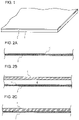
- FIG. 1 is a schematic perspective view of a substrate for a printed circuit board according to an embodiment of the present invention.
- FIG. 2A is a schematic partial sectional view illustrating a coupling agent application step in a method for producing the substrate for a printed circuit board in FIG. 1 .
- FIG. 2B is a schematic partial sectional view illustrating a step in the method for producing the substrate for a printed circuit board in FIG. 1 , the step being performed subsequent to the step illustrated in FIG. 2A .
- FIG. 2C is a schematic partial sectional view illustrating a step in the method for producing the substrate for a printed circuit board in FIG. 1 , the step being performed subsequent to the step illustrated in FIG. 2B .
- FIG. 3A is a schematic partial sectional view illustrating a resist coating step in a method for producing a printed circuit board using the substrate for a printed circuit board in FIG. 1 .
- FIG. 3B is a schematic partial sectional view illustrating a step in the method for producing a printed circuit board using the substrate for a printed circuit board in FIG. 1 , the step being performed subsequent to the step illustrated in FIG. 3A .
- FIG. 3C is a schematic partial sectional view illustrating a step in the method for producing a printed circuit board using the substrate for a printed circuit board in FIG. 1 , the step being performed subsequent to the step illustrated in FIG. 3B .
- FIG. 3D is a schematic partial sectional view illustrating a step in the method for producing a printed circuit board using the substrate for a printed circuit board in FIG. 1 , the step being performed subsequent to the step illustrated in FIG. 3C .
- the substrate for a printed circuit board that has been proposed in the above patent application publication satisfies the requirement for high-density printed circuits in that adhesion strength between the base film and each of the metal layers can be increased.
- the thin copper layers are formed by sputtering in order to make the metal layers closely adhere to the base film. Therefore, vacuum equipment is necessary, which may result in an increase in the costs of, for example, installation, maintenance, and operation of the equipment. As a result, the production cost of the substrate for a printed circuit board increases.
- An object of the present invention is to provide a substrate for a printed circuit board, a printed circuit board, and a method for producing a substrate for a printed circuit board that enable an improvement in adhesion strength between a metal layer and a base film at a low cost.
- the inventors found that the presence of nitrogen between a base film and a metal layer of a substrate for a printed circuit board improves adhesion strength therebetween and that an increase in the amount of this nitrogen present tends to increase the adhesion strength.
- the metal layer can be caused to closely adhere to the base film by controlling the amount of nitrogen present between the base film and the metal layer without using vacuum equipment.
- the substrate for a printed circuit board and the printed circuit board according to the present invention enable an improvement in adhesion strength between the metal layer and the base film at a low cost.
- the method for producing a substrate for a printed circuit board according to the present invention realizes production of a substrate for a printed circuit board at a low cost, the substrate having high adhesion strength between the metal layer and the base film.
- a substrate for a printed circuit board is a substrate for a printed circuit board, the substrate including a base film and a metal layer disposed on at least one of surfaces of the base film.
- an amount of nitrogen present per unit area is 1 atomic % or more and 10 atomic % or less.
- the substrate for a printed circuit board nitrogen is present between the base film and the metal layer. Accordingly, a resin constituting the base film is partially decomposed and turned into radicals by the heating temperature during hot pressing, thereby forming a C—N bond between carbon in the resin and nitrogen between the base film and the metal layer. That is, in the substrate for a printed circuit board, since the amount of nitrogen present on a surface of the base film exposed after removal of the metal layer by etching with an acidic solution is within the above range, such a C—N bond is formed on the surface of the base film in a predetermined amount or more, and high adhesion strength is achieved between the base film and the metal layer.
- the adhesion strength between the base film and the metal layer is reliably obtained as long as nitrogen is present at least between the base film and the metal layer. Therefore, expensive vacuum equipment used for physical vapor deposition such as sputtering is not necessary, and the production cost can be reduced.
- An amount of silicon present per unit area is preferably 1 atomic % or more and 10 atomic % or less. Since nitrogen in the C—N bond has a high bonding strength to silicon, and furthermore, this silicon easily bonds to the metal layer with oxygen therebetween. Therefore, silicon present in an amount within the above range enables the adhesion strength between the base film and the metal layer to further improve.
- the upper limit of a ratio of the amount of silicon present per unit area to the amount of nitrogen present per unit area of the exposed surface of the base film is preferably 4.
- the ratio of the amount of silicon present to the amount of nitrogen present is the upper limit or less, the adhesion strength due to the presence of nitrogen can be improved without making the amount of silicon added excessively large. Thus, the adhesion strength can be easily improved while suppressing an increase in the production cost.
- a coupling agent containing nitrogen or a group derived from the coupling agent is preferably present in the vicinity of an interface between the base film and the metal layer.
- a coupling agent containing nitrogen or a group derived from the coupling agent is present in the vicinity of the interface, the C—N bond can be easily formed to further improve the adhesion strength between the base film and the metal layer.
- the coupling agent is preferably a silane coupling agent.
- a silane coupling agent facilitates bonding between the metal layer and nitrogen in the C—N bond with silicon therebetween and thus improves the adhesion strength between the base film and the metal layer more easily.
- a surface of the metal layer, the surface being disposed on the base film side preferably has a ten-point average roughness Rz of 0.01 ⁇ m or more and 5.0 ⁇ m or less.
- Rz ten-point average roughness
- the base film preferably contains a fluororesin as a main component.
- Use of a base film containing a fluororesin as a main component easily decreases the dielectric constant of the base film. Accordingly, the transmission delay and transmission loss in the metal layer are easily reduced.
- a printed circuit board is a printed circuit board including a base film and a metal pattern disposed on at least one of surfaces of the base film.
- an amount of nitrogen present per unit area is 1 atomic % or more and 10 atomic % or less.
- the printed circuit board is obtained by using the above-described substrate for a printed circuit board, the printed circuit board has high adhesion strength between the base film and the metal pattern and can be produced at a low cost.
- a method for producing a substrate for a printed circuit board is a method for producing a substrate for a printed circuit board, the method including a step of applying a coupling agent containing nitrogen to one of surfaces of a metal layer, a step of stacking a base film on the surface of the metal layer, the surface having the coupling agent applied thereto, and a step of hot-pressing a stacked body of the metal layer and the base film.
- the method for producing a substrate for a printed circuit board includes hot-pressing a stacked body obtained by stacking a base film on a surface of a metal layer, the surface having a coupling agent applied thereto. Accordingly, a resin constituting the base film is partially decomposed and turned into radicals by the heating temperature during this hot pressing, thereby forming a C—N bond between carbon in the resin and nitrogen between the base film and the metal layer. Accordingly, use of the method for producing a substrate for a printed circuit board can provide a substrate for a printed circuit board, the substrate having a high adhesion strength between the base film and the metal layer.
- the method for producing a substrate for a printed circuit board can be performed by applying a coupling agent containing nitrogen, and subsequently performing hot-pressing. Therefore, expensive vacuum equipment used for physical vapor deposition such as sputtering is not necessary, and the production cost can be reduced.
- the term “vicinity of the interface” refers to a region near the interface between the base film and the metal layer and means, for example, a region extending to 500 nm or less from the interface between the base film and the metal layer.
- group derived from the coupling agent refers to a group formed by removing at least one organic functional group, hydrolyzable group, or the like from the coupling agent.
- ten-point average roughness (Rz)” refers to a value measured in accordance with JIS-B0601: 2013 where the evaluation length (l) is 3.2 mm and the cut-off value ( ⁇ c) is 0.8 mm.
- the term “main component” refers to a component that has the highest content and, for example, a component having a content of 50% by mass or more.
- a substrate for a printed circuit board, a printed circuit board, and a method for producing a substrate for a printed circuit board according to embodiments of the present invention will now be described with reference to the drawings.
- a substrate for a printed circuit board in FIG. 1 includes a base film 1 and a metal layer 2 disposed on one of surfaces of the base film 1 . Furthermore, nitrogen is present in the vicinity of the interface between the base film 1 and the metal layer 2 .
- the base film 1 included in the substrate for a printed circuit board has an insulating property.
- the material of the base film 1 include polyethylene terephthalate (PET), polyimides (PI), and fluororesins.
- PET polyethylene terephthalate
- PI polyimides
- fluororesin refers to a resin in which at least one hydrogen atom bonded to a carbon atom that forms a repeating unit of a polymer chain is substituted with a fluorine atom or an organic group having a fluorine atom (hereinafter, may be referred to as a “fluorine atom-containing group”).
- the fluorine atom-containing group is a group in which at least one hydrogen atom in a linear or branched organic group is substituted with a fluorine atom.
- fluorine atom-containing group examples include fluoroalkyl groups, fluoroalkoxy groups, and fluoropolyether groups.
- fluororesins include tetrafluoroethylene-hexafluoropropylene copolymers (FEP), polytetrafluoroethylene (PTFE), tetrafluoroethylene-perfluoroalkyl vinyl ether copolymers (PFA), ethylene-tetrafluoroethylene copolymers (ETFE), polyvinylidene fluoride (PVDF), polychlorotrifluoroethylene (PCTFE), ethylene-chlorotrifluoroethylene copolymers (ECTFE), polyvinyl fluoride (PVF), fluoroelastomers, and fluorothermoplastics (THV) obtained from three monomers of tetrafluoroethylene, hexafluoropropylene, and vinylidene fluoride.
- FEP tetrafluoroethylene-hex
- the thickness of the base film 1 is determined in accordance with a printed circuit board produced by using the substrate for a printed circuit board, and the thickness is not particularly limited.
- the lower limit of the average thickness of the base film 1 is preferably 5 ⁇ m and more preferably 12 ⁇ m.
- the upper limit of the average thickness of the base film 1 is preferably 2 mm and more preferably 1.6 mm.
- the base film 1 may have insufficient strength.
- the average thickness of the base film 1 exceeds the upper limit, a reduction in the thickness of the resulting printed circuit board may become difficult to achieve.
- the metal layer 2 is disposed on one of surfaces of the base film 1 as illustrated in FIG. 1 .
- a main component of the metal layer 2 is preferably a metal having high conductivity.
- the metal include copper, nickel, aluminum, gold, silver, and alloys thereof. Of these, copper or a copper alloy is preferred as a metal having good conductivity and having good adhesiveness to the base film 1 .
- the lower limit of the average thickness of the metal layer 2 is preferably 0.05 ⁇ m and more preferably 0.1 ⁇ m.
- the upper limit of the average thickness of the metal layer 2 is preferably 2 ⁇ m and more preferably 1.5 ⁇ M.
- the metal layer 2 may be easily damaged.
- the average thickness of the metal layer 2 exceeds the upper limit, a reduction in the thickness of the resulting printed circuit board may become difficult to achieve.
- the lower limit of the ten-point average roughness Rz of a surface of the metal layer 2 , the surface being disposed on the base film 1 side, is preferably 0.01 ⁇ m and more preferably 0.05 ⁇ m.
- the upper limit of the ten-point average roughness Rz is preferably 5.0 ⁇ m and more preferably 3.0 ⁇ m.
- the ten-point average roughness Rz is less than the lower limit, the production cost of the printed circuit board may be increased.
- the ten-point average roughness Rz exceeds the upper limit, a decrease in the transmission rate and an increase in the transmission loss may be caused by the skin effect.
- a rust-proofing layer may be formed on a surface of the metal layer 2 .
- the rust-proofing layer suppresses a decrease in the adhesion strength due to oxidation of the surface of the metal layer 2 .
- the rust-proofing layer preferably contains cobalt, chromium, or copper and more preferably contains cobalt or a cobalt alloy as a main component.
- the rust-proofing layer may be formed as a single layer or a plurality of layers.
- the rust-proofing layer may be formed as a plating layer. This plating layer is formed as a single-metal plating layer or an alloy plating layer.
- the metal constituting the single-metal plating layer is preferably cobalt. Examples of the alloy constituting the alloy plating layer include cobalt alloys such as cobalt-molybdenum, cobalt-nickel-tungsten, and cobalt-nickel-germanium.
- Nitrogen is present in the vicinity of the interface between the base film 1 and the metal layer 2 . Since this nitrogen forms a C—N bond with carbon in the resin constituting the base film 1 , the presence of this nitrogen provides high adhesion strength between the metal layer 2 and the base film 1 .
- the amount of nitrogen present in the vicinity of the interface can be determined by the amount of nitrogen present per unit area of a surface of the base film 1 exposed after removal of the metal layer 2 by etching with an acidic solution.
- the amount of nitrogen present per unit area can be determined on the basis of a peak area of a N1s spectrum by using an X-ray photoelectron spectrometer that irradiates a surface of the base film 1 with X-rays and analyzes kinetic energy of photoelectrons emitted from the surface of the base film.
- the lower limit of the amount of nitrogen present per unit area determined as described above is 1 atomic %, preferably 3 atomic %, and more preferably 5 atomic %.
- the upper limit of the amount of nitrogen present per unit area is 10 atomic %, preferably 9 atomic %, and more preferably 8 atomic %.
- the amount of nitrogen present per unit area is less than the lower limit, the number of C—N bonds formed on the surface of the base film 1 is small, and thus predetermined adhesion strength is not obtained between the base film 1 and the metal layer 2 , and the metal layer 2 may become easily separated.
- the amount of nitrogen present per unit area exceeds the upper limit, the production cost of the substrate for a printed circuit board may become excessively high in order to increase the amount of nitrogen present.
- silicon is preferably present in the vicinity of the interface between the base film 1 and the metal layer 2 .
- nitrogen that forms the C—N bond easily bonds to oxygen in the metal layer 2 with the silicon therebetween to enhance the effect of improving adhesion strength due to the presence of nitrogen.
- the amount of silicon present in the vicinity of the interface can be determined by the amount of silicon present per unit area of a surface of the base film 1 exposed after removal of the metal layer 2 by etching with an acidic solution.
- the amount of silicon present per unit area can be determined by a method similar to the above-described method for determining the amount of nitrogen present per unit area. Specifically, the amount of silicon present per unit area can be determined on the basis of a peak area of a Si2p spectrum by using an X-ray photoelectron spectrometer.
- the lower limit of the amount of silicon present per unit area determined as described above is preferably 1 atomic % and more preferably 3.5 atomic %.
- the upper limit of the amount of silicon present per unit area is preferably 10 atomic % and more preferably 5.5 atomic %.
- the lower limit of a ratio of the amount of silicon present per unit area to the amount of nitrogen present per unit area in the XPS analysis is preferably 0.1 and more preferably 0.3.
- the upper limit of the ratio is preferably 4 and more preferably 1.5.
- the ratio is less than the lower limit, the improvement effect due to silicon may not be sufficiently obtained relative to adhesion strength obtained by the presence of nitrogen.
- the ratio exceeds the upper limit, the amount of silicon added becomes excessive relative to the effect of improving the adhesion strength due to the presence of nitrogen. Therefore, the production cost of the substrate for a printed circuit board may be increased.
- An example of a method for causing nitrogen to be present in the vicinity of the interface of the substrate for a printed circuit board is a method in which the base film 1 and the metal layer 2 are laminated with a coupling agent containing nitrogen.
- a coupling agent is applied to a metal foil serving as the metal layer 2 , the base film 1 is then stacked on a surface of the metal foil, the surface having the coupling agent applied thereto, and the resulting stacked body is subjected to hot pressing.
- the substrate for a printed circuit board is prepared by using a coupling agent containing nitrogen in this manner, the coupling agent containing nitrogen or a group derived from the coupling agent is present in the vicinity of the interface between the base film 1 and the metal layer 2 .
- group derived from the coupling agent refers to a group formed by removing at least one organic functional group, hydrolyzable group, or the like from the coupling agent and is, for example, a group formed by removing an alkoxy group from a silane coupling agent having an alkoxy group as a hydrolyzable group.
- the coupling agent containing nitrogen is preferably a silane coupling agent.
- a silane coupling agent enables silicon to be present in the vicinity of the interface between the base film 1 and the metal layer 2 and enables a further improvement in adhesion strength between the base film 1 and the metal layer 2 .
- silane coupling agent examples include N-2-(aminoethyl)-3-aminopropylmethyldimethoxysilane, N-2-(aminoethyl)-3-aminopropyltrimethoxysilane, 3-aminopropyltrimethoxysilane, 3-aminopropyltriethoxysilane, 3-triethoxysilyl-N-(1,3-dimethyl-butylidene) propylamine, N-phenyl-3-aminopropyltrimethoxysilane, N-(vinylbenzyl)-2-aminoethyl-3-aminopropyltrimethoxysilane hydrochloride, and ⁇ -aminopropyltrimethoxysilane.
- the metal layer 2 to which the coupling agent is applied may be a commercially available metal foil or a metal layer prepared by separating a thin metal film formed on a substrate by a known method such as electroplating, electroless plating, sputtering, physical vapor deposition (PVD), or chemical vapor deposition (CVD).
- a known method such as electroplating, electroless plating, sputtering, physical vapor deposition (PVD), or chemical vapor deposition (CVD).
- an oxygen plasma treatment may be employed. Specifically, for example, a surface of the base film 1 is subjected to an oxygen plasma treatment to introduce oxygen element (carbonyl group), and a nucleophilic addition reaction is then caused to this carbonyl group with a primary amine to introduce nitrogen on the surface of the base film 1 . Subsequently, the base film 1 in which nitrogen is introduced and the metal layer 2 are stacked. Thus, nitrogen can be caused to be present in the vicinity of the interface of the substrate for a printed circuit board.
- oxygen element carbonyl group
- a nucleophilic addition reaction is then caused to this carbonyl group with a primary amine to introduce nitrogen on the surface of the base film 1 .
- the base film 1 in which nitrogen is introduced and the metal layer 2 are stacked.
- nitrogen can be caused to be present in the vicinity of the interface of the substrate for a printed circuit board.
- the lower limit of a peel strength between the metal layer 2 and the base film 1 is preferably 0.5 N/cm, more preferably 2 N/cm, and still more preferably 5 N/cm.
- peel strength refers to a value measured in accordance with JIS-K6854-2: 1999.
- a method for producing the substrate for a printed circuit board includes a step of applying a coupling agent containing nitrogen on one of surfaces of a metal layer (coupling agent application step), a step of stacking a base film on a surface of the metal layer, the surface having the coupling agent applied thereto (stacking step), and a step of hot-pressing a stacked body of the metal layer and the base film (hot-pressing step).
- a coupling agent S containing nitrogen is applied to one of surfaces of a metal layer 2 such as a copper foil and dried.
- the coupling agent S can be applied by using a known method such as spray coating, coater coating, dipping, or pouring.
- the lower limit of the amount of the coupling agent S applied is preferably 0.1 mg/m 2 and more preferably 1 mg/m 2 .
- the upper limit of the amount of the coupling agent S applied is preferably 30 mg/m 2 and more preferably 8 mg/m 2 .
- the amount of the coupling agent S applied is less than the lower limit, the effect of improving adhesion strength due to the coupling agent S may not be sufficiently obtained.
- the amount of the coupling agent S applied exceeds the upper limit, the cohesive force of the coupling agent S may decrease, and the resulting coating film may be easily separated.
- a base film 1 is stacked on the surface of the metal layer 2 , the surface having the coupling agent S applied thereto.
- the resulting stacked body of the metal layer 2 and the base film 1 is subjected to hot pressing to bond the metal layer 2 and the base film 1 to each other.
- a resin constituting the base film 1 is partially decomposed and turned into radicals by the heating temperature during this hot pressing, thereby forming a C—N bond between carbon in the resin and nitrogen contained in the coupling agent or a group derived from the coupling agent.
- the lower limit of the heating temperature during the hot pressing is preferably 150° C. and more preferably 160° C.
- the upper limit of the heating temperature is preferably 500° C. and more preferably 450° C.
- the heating temperature is less than the lower limit, the generation of the radicals becomes insufficient, and adhesion strength between the metal layer 2 and the base film 1 may decrease.
- the heating temperature exceeds the upper limit, the base film 1 may be degraded.
- the lower limit of the pressure during the hot pressing is preferably 0.8 MPa and more preferably 1.0 MPa.
- the upper limit of the pressure is preferably 8 MPa and more preferably 3 MPa.
- the pressure is less than the lower limit, the metal layer 2 and the base film 1 are not satisfactorily bonded to each other, and predetermined adhesion strength may not be obtained.
- the pressure exceeds the upper limit, the shear stress applied in the plane direction is increased at the interface between the base film 1 and the metal layer 2 , and thus it may become difficult to maintain a satisfactory bonding state during the pressing.
- the lower limit of the pressing time during the hot pressing is preferably 1 minute and more preferably 10 minutes.
- the upper limit of the pressing time is preferably 1.5 hours and more preferably 1 hour. When the pressing time is less than the lower limit, sufficient adhesion strength between the metal layer 2 and the base film 1 may not be obtained. On the other hand, when the pressing time exceeds the upper limit, the base film 1 may be degraded.
- the printed circuit board includes a base film 1 and a metal pattern 11 disposed on one of surfaces of the base film 1 , as illustrated in FIG. 3D . Since the printed circuit board is formed by using the substrate for a printed circuit board, the amount of nitrogen present per unit area determined on the basis a peak area of a N1s spectrum in XPS analysis of a surface of the base film 1 exposed after removal of the metal pattern 11 by etching with an acidic solution is 1 atomic % or more and 10 atomic % or less. Note that, regarding a polyimide, the amount of nitrogen present is assumed to be a value determined by subtracting an amount of nitrogen present per unit area determined on the basis of a peak area of a N1s spectrum in XPS analysis of the polyimide alone. When the value obtained by the subtraction is a negative value, the amount of nitrogen present is assumed to be 0%.
- a photosensitive resist 10 is formed so as to cover one of surfaces of the substrate for a printed circuit board prepared to have a predetermined size.
- the resist 10 is patterned so as to correspond to a metal pattern by, for example, exposure and development.
- portions of the metal layer 2 other than the metal pattern are removed by etching using the resist 10 as a mask.
- the remaining resist 10 is removed to provide a printed circuit board including the base film 1 having a metal pattern 11 thereon.
- the printed circuit board can be produced by forming a circuit by another known production method such as a semi-additive method. Since the printed circuit board is produced by using the above-described substrate for a printed circuit board, the printed circuit board has high adhesion strength between the base film 1 and the metal layer 2 , and thus the metal pattern 11 is unlikely to separate from the base film 1 .
- the substrate for a printed circuit board since nitrogen is present between a base film and a metal layer, a C—N bond is formed between the nitrogen and carbon in a resin constituting the base film. With this structure, the substrate for a printed circuit board has high adhesion strength between the base film and the metal layer.
- the substrate for a printed circuit board can be produced without using expensive vacuum equipment necessary for physical vapor deposition such as sputtering, the substrate for a printed circuit board can be produced at a low cost.
- the metal layer is disposed on one of surfaces of the base film.
- the substrate may be a double-sided substrate for a printed circuit board, the substrate having the metal layer on each of two surfaces of the base film.
- a metal layer may be formed on each of two surfaces by a formation method similar to that in the above embodiments.
- a metal layer may be formed on the other surface of the substrate for a printed circuit board by another method, the substrate being obtained in the above embodiments.
- a metal layer may be formed by electroplating on the other surface of the substrate for a printed circuit board.
- PI film (“APICAL” available from KANEKA CORPORATION) having an average thickness of 50 ⁇ m and serving as a base film and two copper foils, each of which was obtained by forming a rust-proofing layer on each of two surfaces of a copper foil having an average thickness of 17 ⁇ m, and applying, as a silane coupling agent, N-2-(aminoethyl)-3-aminopropylmethyldimethoxysilane to a surface of one of the rust-proofing layers, were prepared.
- one of the copper foils, the PI film, and the other copper foil were stacked in that order such that the surfaces to which the silane coupling agent was applied were located on the PI film side.
- the resulting stacked body was then subjected to hot pressing with a hot-pressing machine to obtain a substrate for a printed circuit board of No. 1 as an Example.
- the hot pressing was conducted under the conditions of a pressure of 6.0 MPa, a heating temperature of 320° C., and a pressing time of 40 minutes.
- the temperature profile during the hot pressing the temperature was increased from 25° C. to 320° C. over a period of about 90 minutes, maintained at 320° C. for 40 minutes, and then decreased from 320° C. to 25° C.
- a substrate for a printed circuit board of No. 2 was obtained as an Example by the same method as that used in the substrate for a printed circuit board of No. 1 except that a polyethylene terephthalate (PET) film (“G2” available from TEIJIN LIMITED) having an average thickness of 50 ⁇ m was used as a base film, and the heating temperature and the temperature profile during hot pressing were changed as described below.
- PET polyethylene terephthalate
- the heating temperature during hot pressing was 210° C.
- the temperature profile during hot pressing the temperature was increased from 25° C. to 210° C. over a period of about 90 minutes, maintained at 210° C. for 40 minutes, and then decreased from 210° C. to 25° C.
- a substrate for a printed circuit board of No. 3 was obtained as an Example by the same method as that used in the substrate for a printed circuit board of No. 1 except that a polytetrafluoroethylene (PTFE) film (available from CHUKOH CHEMICAL INDUSTRIES, LTD.) having an average thickness of 50 ⁇ m was used as a base film, 3-aminopropyltriethoxysilane was used as a silane coupling agent, and the heating temperature and the temperature profile during hot pressing were changed as described below.
- the heating temperature during hot pressing was 400° C.
- the temperature profile the temperature was increased from 25° C. to 400° C. over a period of about 90 minutes, maintained at 400° C. for 40 minutes, and then decreased from 400° C. to 25° C.
- a substrate for a printed circuit board of No. 4 was obtained as an Example by the same method as that used in the substrate for a printed circuit board of No. 3 except that a tetrafluoroethylene-perfluoroalkyl vinyl ether copolymer (PFA) film (“AF-0050” available from DAIKIN INDUSTRIES, LTD.) having an average thickness of 50 ⁇ m was used as a base film, and the heating temperature and the temperature profile during hot pressing were changed as described below.
- the heating temperature during hot pressing was 300° C.
- the temperature profile the temperature was increased from 25° C. to 300° C. over a period of about 90 minutes, maintained at 300° C. for 40 minutes, and then decreased from 300° C. to 25° C.
- a substrate for a printed circuit board of No. 5 was obtained as an Example by the same method as that used in the substrate for a printed circuit board of No. 3 except that a tetrafluoroethylene-hexafluoropropylene copolymer (FEP) film (“NF-0050” available from DAIKIN INDUSTRIES, LTD.) having an average thickness of 50 ⁇ m was used as a base film, and the heating temperature and the temperature profile during hot pressing were changed as described below.
- the heating temperature during hot pressing was 320° C.
- the temperature profile the temperature was increased from 25° C. to 320° C. over a period of about 90 minutes, maintained at 320° C. for 40 minutes, and then decreased from 320° C. to 25° C.
- a substrate for a printed circuit board of No. 6 was obtained as an Example by the same method as that used in the substrate for a printed circuit board of No. 1 except that the pressure during hot pressing was 1.2 MPa.
- a substrate for a printed circuit board of No. 7 was obtained as an Example by the same method as that used in the substrate for a printed circuit board of No. 2 except that the pressure during hot pressing was 1.2 MPa.
- a substrate for a printed circuit board of No. 8 was obtained as an Example by the same method as that used in the substrate for a printed circuit board of No. 3 except that the pressure during hot pressing was 1.2 MPa.
- a substrate for a printed circuit board of No. 9 was obtained as an Example by the same method as that used in the substrate for a printed circuit board of No. 4 except that the pressure during hot pressing was 1.2 MPa.
- a substrate for a printed circuit board of No. 10 was obtained as an Example by the same method as that used in the substrate for a printed circuit board of No. 5 except that the pressure during hot pressing was 1.2 MPa.
- a substrate for a printed circuit board of No. 11 was obtained as an Example by the same method as that used in the substrate for a printed circuit board of No. 1 except that the heating temperature during hot pressing was 280° C., and regarding the temperature profile, the temperature was increased from 25° C. to 280° C. over a period of about 90 minutes, maintained at 280° C. for 40 minutes, and then decreased from 280° C. to 25° C.
- a substrate for a printed circuit board of No. 12 was obtained as an Example by the same method as that used in the substrate for a printed circuit board of No. 2 except that the heating temperature during hot pressing was 170° C., and regarding the temperature profile, the temperature was increased from 25° C. to 170° C. over a period of about 90 minutes, maintained at 170° C. for 40 minutes, and then decreased from 170° C. to 25° C.
- a substrate for a printed circuit board of No. 13 was obtained as an Example by the same method as that used in the substrate for a printed circuit board of No. 3 except that the heating temperature during hot pressing was 360° C., and regarding the temperature profile, the temperature was increased from 25° C. to 360° C. over a period of about 90 minutes, maintained at 360° C. for 40 minutes, and then decreased from 360° C. to 25° C.
- a substrate for a printed circuit board of No. 14 was obtained as an Example by the same method as that used in the substrate for a printed circuit board of No. 4 except that the heating temperature during hot pressing was 260° C., and regarding the temperature profile, the temperature was increased from 25° C. to 260° C. over a period of about 90 minutes, maintained at 260° C. for 40 minutes, and then decreased from 260° C. to 25° C.
- a substrate for a printed circuit board of No. 15 was obtained as an Example by the same method as that used in the substrate for a printed circuit board of No. 5 except that the heating temperature during hot pressing was 280° C., and regarding the temperature profile, the temperature was increased from 25° C. to 280° C. over a period of about 90 minutes, maintained at 280° C. for 40 minutes, and then decreased from 280° C. to 25° C.
- one of the copper foils, the PI film, and the other copper foil were stacked in that order.
- the resulting stacked body was then subjected to hot pressing with a hot-pressing machine under the same hot-pressing conditions and the same temperature profile as those in No. 1 to obtain a substrate for a printed circuit board of No. 16 as an Example.
- a substrate for a printed circuit board of No. 17 was obtained as an Example by the same method as that used in the substrate for a printed circuit board of No. 16 except that a PET film which had an average thickness of 50 ⁇ m and in which nitrogen element was introduced on surfaces thereof by the same method as that used in No. 16 was used as a base film, and hot pressing was conducted under the same hot-pressing conditions and the same temperature profile as those in No. 2.
- a substrate for a printed circuit board of No. 18 was obtained as an Example by the same method as that used in the substrate for a printed circuit board of No. 16 except that a PTFE film which had an average thickness of 50 ⁇ m and in which nitrogen element was introduced on surfaces thereof by the same method as that used in No. 16 was used as a base film, and hot pressing was conducted under the same hot-pressing conditions and the same temperature profile as those in No. 3.
- a substrate for a printed circuit board of No. 19 was obtained as an Example by the same method as that used in the substrate for a printed circuit board of No. 16 except that a PFA film which had an average thickness of 50 ⁇ m and in which nitrogen element was introduced on surfaces thereof by the same method as that used in No. 16 was used as a base film, and hot pressing was conducted under the same hot-pressing conditions and the same temperature profile as those in No. 4.
- a substrate for a printed circuit board of No. 20 was obtained as an Example by the same method as that used in the substrate for a printed circuit board of No. 16 except that an FEP film which had an average thickness of 50 ⁇ m and in which nitrogen element was introduced on surfaces thereof by the same method as that used in No. 16 was used as a base film, and hot pressing was conducted under the same hot-pressing conditions and the same temperature profile as those in No. 5.
- a substrate for a printed circuit board of No. 21 was obtained as a Comparative Example by the same method as that used in the substrate for a printed circuit board of No. 1 except that 3-glycidoxypropyltriethoxysilane, which does not contain nitrogen, was used as a silane coupling agent applied to a surface of one of the rust-proofing layers of each of the copper foils.
- a substrate for a printed circuit board of No. 22 was obtained as a Comparative Example by the same method as that used in the substrate for a printed circuit board of No. 2 except that 3-glycidoxypropyltriethoxysilane, which does not contain nitrogen, was used as a silane coupling agent applied to a surface of one of the rust-proofing layers of each of the copper foils.
- a substrate for a printed circuit board of No. 23 was obtained as a Comparative Example by the same method as that used in the substrate for a printed circuit board of No. 3 except that 3-glycidoxypropyltriethoxysilane, which does not contain nitrogen, was used as a silane coupling agent applied to a surface of one of the rust-proofing layers of each of the copper foils.
- a substrate for a printed circuit board of No. 24 was obtained as a Comparative Example by the same method as that used in the substrate for a printed circuit board of No. 4 except that 3-glycidoxypropyltriethoxysilane, which does not contain nitrogen, was used as a silane coupling agent applied to a surface of one of the rust-proofing layers of each of the copper foils.
- a substrate for a printed circuit board of No. 25 was obtained as a Comparative Example by the same method as that used in the substrate for a printed circuit board of No. 5 except that 3-glycidoxypropyltriethoxysilane, which does not contain nitrogen, was used as a silane coupling agent applied to a surface of one of the rust-proofing layers of each of the copper foils.
- the copper foils of the substrates for printed circuit boards of Nos. 1 to 25 were removed with an etchant formed of an acidic solution.
- a surface of each of the base films after the removal of the copper foils was irradiated with X-rays, and the amounts of nitrogen and silicon present on the surface of the base film were measured on the basis of kinetic energy of photoelectrons emitted from the surface of the base film by using an X-ray photoelectron spectrometer (“Quantera SXM” available from ULVAC-PHI, INCORPORATED).
- the amount [atomic %] of nitrogen present per unit area was determined on the basis of the peak area of the N1s spectrum, and the amount [atomic %] of silicon present per unit area was determined on the basis of the peak area of the Si2p spectrum.
- Table 1 shows the measurement results of the amounts of nitrogen and silicon present.
- Table 1 also shows the ratio of the amount of silicon present to the amount of nitrogen present (amount of Si present/amount of N present) obtained from these measurements.
- Nos. 21 to 25 since the amount of nitrogen present was zero, the ratio of the amounts present is not calculated.
- the amount of nitrogen present is assumed to be a value determined by subtracting an amount of nitrogen present per unit area determined on the basis of the peak area of the N1s spectrum in XPS analysis of the polyimide alone.
- the amount of nitrogen present is assumed to be 0%.
- a peel strength (N/cm) between the base film and the copper foil was measured to evaluate the adhesion strength between the base film and the copper foil.
- the peel strength was measured by the method according to JIS-K6854-2: 1999 “Adhesives-Determination of peel strength of bonded assemblies-Part 2: 180° peel”. Table 1 shows the measurement results of the peel strength.
- Nos. 6 to 10 in which the pressure during hot pressing is 1.2 MPa, each have a larger amount of nitrogen present and a higher peel strength than Nos. 1 to 5, in which the pressure during hot pressing is 6.0 MPa.
- the reason for this is believed to be as follows. An increase in the pressure during hot pressing increases the shear stress applied in the plane direction at the interface between the base film and the copper foil, and therefore, in Nos. 1 to 5, a satisfactory bonding state between the base film and the copper foil could not be maintained during hot pressing.
- Nos. 1 to 5 Comparing Nos. 1 to 5 and Nos. 11 to 15, it is found that Nos. 1 to 5, in which the heating temperatures during hot pressing are 40° C. higher than those in Nos. 11 to 15, respectively, each have a larger amount of nitrogen present and a higher peel strength than Nos. 11 to 15. These results show that the amount of nitrogen present can be adjusted by controlling the temperature during hot pressing.
Landscapes
- Engineering & Computer Science (AREA)
- Microelectronics & Electronic Packaging (AREA)
- Manufacturing & Machinery (AREA)
- Manufacturing Of Printed Wiring (AREA)
- Laminated Bodies (AREA)
Abstract
Description
- PTL 1: Japanese Unexamined Patent Application Publication No. 9-136378
| TABLE 1 | |||||||||
| Amount of | |||||||||
| Heating | Pressing | Amount of | Amount of | Si present/ | Peel | ||||
| Base film | Pressure | temperature | time | N present | Si present | Amount of | strength | ||
| No. | material | Coupling agent | (MPa) | (° C.) | (min) | (atomic %) | (atomic %) | N present | (N/cm) |
| 1 | PI | N-2-(Aminoethyl)-3- | 6 | 320 | 40 | 4.3 | 4.3 | 1.00 | 8.1 |
| aminopropylmethyldimethoxysilane | |||||||||
| 2 | PET | N-2-(Aminoethyl)-3- | 6 | 210 | 40 | 4.6 | 4.9 | 1.07 | 11.3 |
| aminopropylmethyldimethoxysilane | |||||||||
| 3 | PTFE | 3-aminopropyltriethoxysilane | 6 | 400 | 40 | 4.2 | 4.0 | 0.95 | 13.0 |
| 4 | PFA | 3-aminopropyltriethoxysilane | 6 | 300 | 40 | 4.5 | 4.3 | 0.96 | 11.1 |
| 5 | FEP | 3-aminopropyltriethoxysilane | 6 | 320 | 40 | 4.3 | 4.5 | 1.05 | 12.2 |
| 6 | PI | N-2-(Aminoethyl)-3- | 1.2 | 320 | 40 | 9.4 | 4.7 | 0.50 | 9.1 |
| aminopropylmethyldimethoxysilane | |||||||||
| 7 | PET | N-2-(Aminoethyl)-3- | 1.2 | 210 | 40 | 9.5 | 4.6 | 0.48 | 15.2 |
| aminopropylmethyldimethoxysilane | |||||||||
| 8 | PTFE | 3-aminopropyltriethoxysilane | 1.2 | 400 | 40 | 9.6 | 4.6 | 0.48 | 17.3 |
| 9 | PFA | 3-aminopropyltriethoxysilane | 1.2 | 300 | 40 | 9.7 | 4.8 | 0.49 | 16.2 |
| 10 | FEP | 3-aminopropyltriethoxysilane | 1.2 | 320 | 40 | 9.6 | 4.8 | 0.50 | 18.4 |
| 11 | PI | N-2-(Aminoethyl)-3- | 6 | 280 | 40 | 1.3 | 4.7 | 3.62 | 5.1 |
| aminopropylmethyldimethoxysilane | |||||||||
| 12 | PET | N-2-(Aminoethyl)-3- | 6 | 170 | 40 | 1.6 | 4.6 | 2.88 | 6.3 |
| aminopropylmethyldimethoxysilane | |||||||||
| 13 | PTFE | 3-aminopropyltriethoxysilane | 6 | 360 | 40 | 1.8 | 4.6 | 2.56 | 7.1 |
| 14 | PFA | 3-aminopropyltriethoxysilane | 6 | 260 | 40 | 1.3 | 4.2 | 3.23 | 6.2 |
| 15 | FEP | 3-aminopropyltriethoxysilane | 6 | 280 | 40 | 1.2 | 4.1 | 3.42 | 7.2 |
| 16 | PI | 6 | 320 | 40 | 4.1 | 0 | 0 | 6.5 | |
| 17 | PET | 6 | 210 | 40 | 4.1 | 0 | 0 | 7.7 | |
| 18 | PTFE | 6 | 400 | 40 | 4.2 | 0 | 0 | 5.8 | |
| 19 | PFA | 6 | 300 | 40 | 4.3 | 0 | 0 | 6.2 | |
| 20 | FEP | 6 | 320 | 40 | 4.4 | 0 | 0 | 7.3 | |
| 21 | PI | 3-glycidoxypropyltriethoxysilane | 6 | 320 | 40 | 0 | 4.2 | — | 0.2 |
| 22 | PET | 3-glycidoxypropyltriethoxysilane | 6 | 210 | 40 | 0 | 4.3 | — | 0.3 |
| 23 | PTFE | 3-glycidoxypropyltriethoxysilane | 6 | 400 | 40 | 0 | 4.2 | — | 0.2 |
| 24 | PFA | 3-glycidoxypropyltriethoxysilane | 6 | 300 | 40 | 0 | 4.1 | — | 0.1 |
| 25 | FEP | 3-glycidoxypropyltriethoxysilane | 6 | 320 | 40 | 0 | 4.6 | — | 0.4 |
[Evaluation Results]
| 1 | |
2 | |
10 | resist |
| 11 | metal pattern | S | coupling agent | ||
Claims (7)
Applications Claiming Priority (4)
| Application Number | Priority Date | Filing Date | Title |
|---|---|---|---|
| JP2015164234 | 2015-08-21 | ||
| JP2015-164234 | 2015-08-21 | ||
| JPJP2015-164234 | 2015-08-21 | ||
| PCT/JP2016/073212 WO2017033713A1 (en) | 2015-08-21 | 2016-08-06 | Printed-wiring board substrate, printed-wiring board, and method for producing printed-wiring board substrate |
Publications (2)
| Publication Number | Publication Date |
|---|---|
| US20180242450A1 US20180242450A1 (en) | 2018-08-23 |
| US11375615B2 true US11375615B2 (en) | 2022-06-28 |
Family
ID=58099911
Family Applications (1)
| Application Number | Title | Priority Date | Filing Date |
|---|---|---|---|
| US15/753,017 Active 2037-11-05 US11375615B2 (en) | 2015-08-21 | 2016-08-06 | Substrate for printed circuit board, printed circuit board, and method for producing substrate for printed circuit board |
Country Status (5)
| Country | Link |
|---|---|
| US (1) | US11375615B2 (en) |
| EP (1) | EP3340755B1 (en) |
| JP (2) | JP6717835B2 (en) |
| CN (1) | CN107852828B (en) |
| WO (1) | WO2017033713A1 (en) |
Families Citing this family (4)
| Publication number | Priority date | Publication date | Assignee | Title |
|---|---|---|---|---|
| EP3340755B1 (en) * | 2015-08-21 | 2024-02-14 | Sumitomo Electric Industries, Ltd. | Printed-wiring board substrate, printed-wiring board, and method for producing printed-wiring board substrate |
| JP7531109B2 (en) * | 2018-10-05 | 2024-08-09 | パナソニックIpマネジメント株式会社 | Metal-clad laminates, wiring boards, and resin-coated metal foils |
| CN116829348A (en) * | 2021-02-19 | 2023-09-29 | 三井金属矿业株式会社 | Manufacturing method of laminated plate and heating element and defroster |
| JP7514808B2 (en) * | 2021-09-10 | 2024-07-11 | 信越化学工業株式会社 | Low dielectric substrate and its manufacturing method |
Citations (16)
| Publication number | Priority date | Publication date | Assignee | Title |
|---|---|---|---|---|
| JPH09136378A (en) | 1995-11-14 | 1997-05-27 | Mitsui Toatsu Chem Inc | Copper thin film substrate and printed wiring board |
| US20050121229A1 (en) * | 2002-03-05 | 2005-06-09 | Kenji Takai | Metal foil with resin and metal-clad laminate, and printed wiring board using the same and method for production thereof |
| US20050202261A1 (en) * | 2004-01-30 | 2005-09-15 | Kenji Takai | Adhesion assisting agent-bearing metal foil, printed wiring board, and production method of printed wiring board |
| US20070196675A1 (en) * | 2004-03-23 | 2007-08-23 | Ube Industries, Ltd. | Adhesion-Enhanced Polyimide Film, Process for Its Production, And Laminated Body |
| WO2008004520A1 (en) | 2006-07-04 | 2008-01-10 | Nippon Steel Chemical Co., Ltd. | Method of modifying surface of polyimide resin layer and process for producing metal-clad laminate |
| JP2008063560A (en) | 2006-07-04 | 2008-03-21 | Nippon Steel Chem Co Ltd | Method for modifying surface of polyimide resin layer and method for producing metal-clad laminate |
| US20100203324A1 (en) * | 2006-07-27 | 2010-08-12 | Ube Industries, Ltd. | Laminate of heat resistant film and metal foil, and method for production thereof |
| US20110189501A1 (en) * | 2008-07-22 | 2011-08-04 | Furukawa Electric Co., Ltd. | Flexible copper clad laminate |
| WO2011122645A1 (en) | 2010-03-30 | 2011-10-06 | Jx日鉱日石金属株式会社 | Copper foil for printed wiring board with excellent etching properties and layered body using same |
| JP2014111824A (en) | 2012-09-10 | 2014-06-19 | Jx Nippon Mining & Metals Corp | Surface-treated copper foil and laminate made therefrom |
| US20150079415A1 (en) * | 2012-03-29 | 2015-03-19 | Jx Nippon Mining & Metals Corporation | Surface-Treated Copper Foil |
| JP2015065388A (en) | 2013-09-26 | 2015-04-09 | 大日本印刷株式会社 | Collector sheet for solar cell module and manufacturing method therefor |
| CN104603333A (en) | 2012-09-10 | 2015-05-06 | Jx日矿日石金属株式会社 | Surface-treated copper foil and laminated board using same |
| JP2015097257A (en) | 2013-10-11 | 2015-05-21 | 住友電工プリントサーキット株式会社 | Fluorine resin base material, printed wiring board, and circuit module |
| JP2015115422A (en) | 2013-12-10 | 2015-06-22 | 住友電工プリントサーキット株式会社 | Printed wiring board |
| US20160250830A1 (en) | 2013-10-11 | 2016-09-01 | Sumitomo Electric Printed Circuits, Inc. | Fluororesin base material, printed wiring board, and circuit module |
Family Cites Families (3)
| Publication number | Priority date | Publication date | Assignee | Title |
|---|---|---|---|---|
| WO2014192718A1 (en) * | 2013-05-31 | 2014-12-04 | 住友電気工業株式会社 | Metal-resin composite body, wiring material, and method for producing metal-resin composite body |
| JP6256832B2 (en) * | 2013-12-27 | 2018-01-10 | 住友電工プリントサーキット株式会社 | Printed wiring board for strain gauge |
| EP3340755B1 (en) * | 2015-08-21 | 2024-02-14 | Sumitomo Electric Industries, Ltd. | Printed-wiring board substrate, printed-wiring board, and method for producing printed-wiring board substrate |
-
2016
- 2016-08-06 EP EP16839060.7A patent/EP3340755B1/en active Active
- 2016-08-06 CN CN201680041829.3A patent/CN107852828B/en active Active
- 2016-08-06 WO PCT/JP2016/073212 patent/WO2017033713A1/en not_active Ceased
- 2016-08-06 US US15/753,017 patent/US11375615B2/en active Active
- 2016-08-06 JP JP2017536723A patent/JP6717835B2/en active Active
-
2020
- 2020-04-13 JP JP2020071861A patent/JP6950036B2/en active Active
Patent Citations (16)
| Publication number | Priority date | Publication date | Assignee | Title |
|---|---|---|---|---|
| JPH09136378A (en) | 1995-11-14 | 1997-05-27 | Mitsui Toatsu Chem Inc | Copper thin film substrate and printed wiring board |
| US20050121229A1 (en) * | 2002-03-05 | 2005-06-09 | Kenji Takai | Metal foil with resin and metal-clad laminate, and printed wiring board using the same and method for production thereof |
| US20050202261A1 (en) * | 2004-01-30 | 2005-09-15 | Kenji Takai | Adhesion assisting agent-bearing metal foil, printed wiring board, and production method of printed wiring board |
| US20070196675A1 (en) * | 2004-03-23 | 2007-08-23 | Ube Industries, Ltd. | Adhesion-Enhanced Polyimide Film, Process for Its Production, And Laminated Body |
| WO2008004520A1 (en) | 2006-07-04 | 2008-01-10 | Nippon Steel Chemical Co., Ltd. | Method of modifying surface of polyimide resin layer and process for producing metal-clad laminate |
| JP2008063560A (en) | 2006-07-04 | 2008-03-21 | Nippon Steel Chem Co Ltd | Method for modifying surface of polyimide resin layer and method for producing metal-clad laminate |
| US20100203324A1 (en) * | 2006-07-27 | 2010-08-12 | Ube Industries, Ltd. | Laminate of heat resistant film and metal foil, and method for production thereof |
| US20110189501A1 (en) * | 2008-07-22 | 2011-08-04 | Furukawa Electric Co., Ltd. | Flexible copper clad laminate |
| WO2011122645A1 (en) | 2010-03-30 | 2011-10-06 | Jx日鉱日石金属株式会社 | Copper foil for printed wiring board with excellent etching properties and layered body using same |
| US20150079415A1 (en) * | 2012-03-29 | 2015-03-19 | Jx Nippon Mining & Metals Corporation | Surface-Treated Copper Foil |
| JP2014111824A (en) | 2012-09-10 | 2014-06-19 | Jx Nippon Mining & Metals Corp | Surface-treated copper foil and laminate made therefrom |
| CN104603333A (en) | 2012-09-10 | 2015-05-06 | Jx日矿日石金属株式会社 | Surface-treated copper foil and laminated board using same |
| JP2015065388A (en) | 2013-09-26 | 2015-04-09 | 大日本印刷株式会社 | Collector sheet for solar cell module and manufacturing method therefor |
| JP2015097257A (en) | 2013-10-11 | 2015-05-21 | 住友電工プリントサーキット株式会社 | Fluorine resin base material, printed wiring board, and circuit module |
| US20160250830A1 (en) | 2013-10-11 | 2016-09-01 | Sumitomo Electric Printed Circuits, Inc. | Fluororesin base material, printed wiring board, and circuit module |
| JP2015115422A (en) | 2013-12-10 | 2015-06-22 | 住友電工プリントサーキット株式会社 | Printed wiring board |
Also Published As
| Publication number | Publication date |
|---|---|
| CN107852828B (en) | 2020-03-17 |
| JP6950036B2 (en) | 2021-10-13 |
| EP3340755B1 (en) | 2024-02-14 |
| JPWO2017033713A1 (en) | 2018-06-07 |
| CN107852828A (en) | 2018-03-27 |
| JP2020120122A (en) | 2020-08-06 |
| US20180242450A1 (en) | 2018-08-23 |
| EP3340755A1 (en) | 2018-06-27 |
| WO2017033713A1 (en) | 2017-03-02 |
| JP6717835B2 (en) | 2020-07-08 |
| EP3340755A4 (en) | 2018-08-08 |
Similar Documents
| Publication | Publication Date | Title |
|---|---|---|
| CN107614760B (en) | Roughening treatment copper foil, copper-clad laminated board and printed circuit board | |
| JP6393619B2 (en) | Multilayer printed wiring board manufacturing method and base substrate | |
| JP6950036B2 (en) | Manufacturing method of printed wiring board board, printed wiring board and printed wiring board board | |
| JP6905157B2 (en) | Roughened copper foil, copper foil with carrier, copper-clad laminate and printed wiring board | |
| JP6687765B2 (en) | Metal foil with carrier | |
| JP2016079346A (en) | Resin film, coverlay for printed wiring board, substrate for printed wiring board and printed wiring board | |
| TWI619413B (en) | Method for manufacturing printed wiring board, surface-treated copper foil, laminated body, printed wiring board, semiconductor package, and electronic device | |
| JP7259093B2 (en) | Roughened copper foil, copper foil with carrier, copper clad laminate and printed wiring board | |
| JP6104260B2 (en) | Metal foil with carrier | |
| JP2010218905A (en) | Metal material for substrate, surface roughening treatment of metal material for substrate, and manufacturing method of metal material for substrate | |
| JP7834086B2 (en) | Roughened copper foil, copper-clad laminates, and printed circuit boards | |
| WO2022014647A1 (en) | Manufacturing methods for copper-clad laminate and printed wiring board | |
| JP7834085B2 (en) | Roughened copper foil, copper-clad laminates, and printed circuit boards | |
| KR20180111660A (en) | Copper foil with release layer, laminate, method of manufacturing printed wiring board and method of manufacturing electronic device | |
| WO2022014648A1 (en) | Copper-clad laminate plate and printed wiring board | |
| CN117441039A (en) | Roughening of copper foil, copper-clad laminates and printed circuit boards | |
| TW202248459A (en) | Roughened copper foil, copper-clad laminate board, and printed circuit board | |
| WO2021166513A1 (en) | Surface-treated metal foil and metal-clad laminate | |
| JP2013256053A (en) | Metal resin laminate and method of manufacturing the same |
Legal Events
| Date | Code | Title | Description |
|---|---|---|---|
| AS | Assignment |
Owner name: SUMITOMO ELECTRIC INDUSTRIES, LTD., JAPAN Free format text: ASSIGNMENT OF ASSIGNORS INTEREST;ASSIGNORS:YAMANAKA, YUICHIRO;OKA, YOSHIO;KIYA, SATOSHI;AND OTHERS;SIGNING DATES FROM 20171219 TO 20180110;REEL/FRAME:044943/0742 Owner name: SUMITOMO ELECTRIC FINE POLYMER, INC., JAPAN Free format text: ASSIGNMENT OF ASSIGNORS INTEREST;ASSIGNORS:YAMANAKA, YUICHIRO;OKA, YOSHIO;KIYA, SATOSHI;AND OTHERS;SIGNING DATES FROM 20171219 TO 20180110;REEL/FRAME:044943/0742 Owner name: SUMITOMO ELECTRIC PRINTED CIRCUITS, INC., JAPAN Free format text: ASSIGNMENT OF ASSIGNORS INTEREST;ASSIGNORS:YAMANAKA, YUICHIRO;OKA, YOSHIO;KIYA, SATOSHI;AND OTHERS;SIGNING DATES FROM 20171219 TO 20180110;REEL/FRAME:044943/0742 |
|
| FEPP | Fee payment procedure |
Free format text: ENTITY STATUS SET TO UNDISCOUNTED (ORIGINAL EVENT CODE: BIG.); ENTITY STATUS OF PATENT OWNER: LARGE ENTITY |
|
| STPP | Information on status: patent application and granting procedure in general |
Free format text: DOCKETED NEW CASE - READY FOR EXAMINATION |
|
| STPP | Information on status: patent application and granting procedure in general |
Free format text: NON FINAL ACTION MAILED |
|
| STPP | Information on status: patent application and granting procedure in general |
Free format text: RESPONSE TO NON-FINAL OFFICE ACTION ENTERED AND FORWARDED TO EXAMINER |
|
| STPP | Information on status: patent application and granting procedure in general |
Free format text: RESPONSE TO NON-FINAL OFFICE ACTION ENTERED AND FORWARDED TO EXAMINER |
|
| STPP | Information on status: patent application and granting procedure in general |
Free format text: NOTICE OF ALLOWANCE MAILED -- APPLICATION RECEIVED IN OFFICE OF PUBLICATIONS |
|
| STPP | Information on status: patent application and granting procedure in general |
Free format text: PUBLICATIONS -- ISSUE FEE PAYMENT RECEIVED |
|
| STPP | Information on status: patent application and granting procedure in general |
Free format text: PUBLICATIONS -- ISSUE FEE PAYMENT VERIFIED |
|
| STCF | Information on status: patent grant |
Free format text: PATENTED CASE |
|
| MAFP | Maintenance fee payment |
Free format text: PAYMENT OF MAINTENANCE FEE, 4TH YEAR, LARGE ENTITY (ORIGINAL EVENT CODE: M1551); ENTITY STATUS OF PATENT OWNER: LARGE ENTITY Year of fee payment: 4 |