US11366637B2 - Multiplexing between different processing channels - Google Patents
Multiplexing between different processing channels Download PDFInfo
- Publication number
- US11366637B2 US11366637B2 US17/351,449 US202117351449A US11366637B2 US 11366637 B2 US11366637 B2 US 11366637B2 US 202117351449 A US202117351449 A US 202117351449A US 11366637 B2 US11366637 B2 US 11366637B2
- Authority
- US
- United States
- Prior art keywords
- input
- logic unit
- output
- processing channel
- line
- Prior art date
- Legal status (The legal status is an assumption and is not a legal conclusion. Google has not performed a legal analysis and makes no representation as to the accuracy of the status listed.)
- Active
Links
- 238000012545 processing Methods 0.000 title claims abstract description 254
- 238000004519 manufacturing process Methods 0.000 claims description 58
- 238000000034 method Methods 0.000 claims description 37
- 230000004044 response Effects 0.000 claims description 23
- 239000012634 fragment Substances 0.000 description 28
- 230000008569 process Effects 0.000 description 10
- 238000013459 approach Methods 0.000 description 6
- 238000010586 diagram Methods 0.000 description 6
- 230000003068 static effect Effects 0.000 description 5
- 230000006872 improvement Effects 0.000 description 4
- 238000004590 computer program Methods 0.000 description 3
- 230000001960 triggered effect Effects 0.000 description 3
- XUIMIQQOPSSXEZ-UHFFFAOYSA-N Silicon Chemical compound [Si] XUIMIQQOPSSXEZ-UHFFFAOYSA-N 0.000 description 2
- 230000008901 benefit Effects 0.000 description 2
- 238000004422 calculation algorithm Methods 0.000 description 2
- 230000008878 coupling Effects 0.000 description 2
- 238000010168 coupling process Methods 0.000 description 2
- 238000005859 coupling reaction Methods 0.000 description 2
- 238000013461 design Methods 0.000 description 2
- 230000000694 effects Effects 0.000 description 2
- 230000006870 function Effects 0.000 description 2
- 238000012986 modification Methods 0.000 description 2
- 230000004048 modification Effects 0.000 description 2
- 230000003287 optical effect Effects 0.000 description 2
- 229910052710 silicon Inorganic materials 0.000 description 2
- 239000010703 silicon Substances 0.000 description 2
- 238000012360 testing method Methods 0.000 description 2
- 241000613118 Gryllus integer Species 0.000 description 1
- 238000013528 artificial neural network Methods 0.000 description 1
- 230000006399 behavior Effects 0.000 description 1
- 238000004364 calculation method Methods 0.000 description 1
- 238000012993 chemical processing Methods 0.000 description 1
- 238000004891 communication Methods 0.000 description 1
- 239000004020 conductor Substances 0.000 description 1
- 239000000470 constituent Substances 0.000 description 1
- 238000002955 isolation Methods 0.000 description 1
- 238000013507 mapping Methods 0.000 description 1
- 230000000630 rising effect Effects 0.000 description 1
- 239000004065 semiconductor Substances 0.000 description 1
- 238000005389 semiconductor device fabrication Methods 0.000 description 1
- 238000012546 transfer Methods 0.000 description 1
Images


Classifications
-
- G—PHYSICS
- G06—COMPUTING; CALCULATING OR COUNTING
- G06F—ELECTRIC DIGITAL DATA PROCESSING
- G06F7/00—Methods or arrangements for processing data by operating upon the order or content of the data handled
- G06F7/38—Methods or arrangements for performing computations using exclusively denominational number representation, e.g. using binary, ternary, decimal representation
- G06F7/48—Methods or arrangements for performing computations using exclusively denominational number representation, e.g. using binary, ternary, decimal representation using non-contact-making devices, e.g. tube, solid state device; using unspecified devices
- G06F7/544—Methods or arrangements for performing computations using exclusively denominational number representation, e.g. using binary, ternary, decimal representation using non-contact-making devices, e.g. tube, solid state device; using unspecified devices for evaluating functions by calculation
- G06F7/5443—Sum of products
-
- G—PHYSICS
- G06—COMPUTING; CALCULATING OR COUNTING
- G06F—ELECTRIC DIGITAL DATA PROCESSING
- G06F9/00—Arrangements for program control, e.g. control units
- G06F9/06—Arrangements for program control, e.g. control units using stored programs, i.e. using an internal store of processing equipment to receive or retain programs
- G06F9/30—Arrangements for executing machine instructions, e.g. instruction decode
- G06F9/38—Concurrent instruction execution, e.g. pipeline or look ahead
- G06F9/3802—Instruction prefetching
- G06F9/3808—Instruction prefetching for instruction reuse, e.g. trace cache, branch target cache
-
- G—PHYSICS
- G06—COMPUTING; CALCULATING OR COUNTING
- G06F—ELECTRIC DIGITAL DATA PROCESSING
- G06F9/00—Arrangements for program control, e.g. control units
- G06F9/06—Arrangements for program control, e.g. control units using stored programs, i.e. using an internal store of processing equipment to receive or retain programs
- G06F9/30—Arrangements for executing machine instructions, e.g. instruction decode
- G06F9/38—Concurrent instruction execution, e.g. pipeline or look ahead
- G06F9/3824—Operand accessing
-
- G—PHYSICS
- G06—COMPUTING; CALCULATING OR COUNTING
- G06T—IMAGE DATA PROCESSING OR GENERATION, IN GENERAL
- G06T1/00—General purpose image data processing
- G06T1/20—Processor architectures; Processor configuration, e.g. pipelining
-
- G—PHYSICS
- G06—COMPUTING; CALCULATING OR COUNTING
- G06F—ELECTRIC DIGITAL DATA PROCESSING
- G06F15/00—Digital computers in general; Data processing equipment in general
- G06F15/76—Architectures of general purpose stored program computers
- G06F15/80—Architectures of general purpose stored program computers comprising an array of processing units with common control, e.g. single instruction multiple data processors
-
- G—PHYSICS
- G06—COMPUTING; CALCULATING OR COUNTING
- G06F—ELECTRIC DIGITAL DATA PROCESSING
- G06F7/00—Methods or arrangements for processing data by operating upon the order or content of the data handled
- G06F7/38—Methods or arrangements for performing computations using exclusively denominational number representation, e.g. using binary, ternary, decimal representation
- G06F7/48—Methods or arrangements for performing computations using exclusively denominational number representation, e.g. using binary, ternary, decimal representation using non-contact-making devices, e.g. tube, solid state device; using unspecified devices
- G06F7/52—Multiplying; Dividing
- G06F7/523—Multiplying only
-
- G—PHYSICS
- G06—COMPUTING; CALCULATING OR COUNTING
- G06F—ELECTRIC DIGITAL DATA PROCESSING
- G06F9/00—Arrangements for program control, e.g. control units
- G06F9/06—Arrangements for program control, e.g. control units using stored programs, i.e. using an internal store of processing equipment to receive or retain programs
- G06F9/30—Arrangements for executing machine instructions, e.g. instruction decode
- G06F9/30003—Arrangements for executing specific machine instructions
- G06F9/30007—Arrangements for executing specific machine instructions to perform operations on data operands
- G06F9/3001—Arithmetic instructions
-
- G—PHYSICS
- G06—COMPUTING; CALCULATING OR COUNTING
- G06F—ELECTRIC DIGITAL DATA PROCESSING
- G06F9/00—Arrangements for program control, e.g. control units
- G06F9/06—Arrangements for program control, e.g. control units using stored programs, i.e. using an internal store of processing equipment to receive or retain programs
- G06F9/30—Arrangements for executing machine instructions, e.g. instruction decode
- G06F9/30003—Arrangements for executing specific machine instructions
- G06F9/30007—Arrangements for executing specific machine instructions to perform operations on data operands
- G06F9/30029—Logical and Boolean instructions, e.g. XOR, NOT
-
- G—PHYSICS
- G06—COMPUTING; CALCULATING OR COUNTING
- G06F—ELECTRIC DIGITAL DATA PROCESSING
- G06F9/00—Arrangements for program control, e.g. control units
- G06F9/06—Arrangements for program control, e.g. control units using stored programs, i.e. using an internal store of processing equipment to receive or retain programs
- G06F9/30—Arrangements for executing machine instructions, e.g. instruction decode
- G06F9/30145—Instruction analysis, e.g. decoding, instruction word fields
-
- G—PHYSICS
- G06—COMPUTING; CALCULATING OR COUNTING
- G06F—ELECTRIC DIGITAL DATA PROCESSING
- G06F9/00—Arrangements for program control, e.g. control units
- G06F9/06—Arrangements for program control, e.g. control units using stored programs, i.e. using an internal store of processing equipment to receive or retain programs
- G06F9/30—Arrangements for executing machine instructions, e.g. instruction decode
- G06F9/38—Concurrent instruction execution, e.g. pipeline or look ahead
- G06F9/3885—Concurrent instruction execution, e.g. pipeline or look ahead using a plurality of independent parallel functional units
- G06F9/3889—Concurrent instruction execution, e.g. pipeline or look ahead using a plurality of independent parallel functional units controlled by multiple instructions, e.g. MIMD, decoupled access or execute
-
- H—ELECTRICITY
- H03—ELECTRONIC CIRCUITRY
- H03K—PULSE TECHNIQUE
- H03K19/00—Logic circuits, i.e. having at least two inputs acting on one output; Inverting circuits
- H03K19/0008—Arrangements for reducing power consumption
-
- H—ELECTRICITY
- H03—ELECTRONIC CIRCUITRY
- H03K—PULSE TECHNIQUE
- H03K19/00—Logic circuits, i.e. having at least two inputs acting on one output; Inverting circuits
- H03K19/02—Logic circuits, i.e. having at least two inputs acting on one output; Inverting circuits using specified components
- H03K19/173—Logic circuits, i.e. having at least two inputs acting on one output; Inverting circuits using specified components using elementary logic circuits as components
- H03K19/1733—Controllable logic circuits
- H03K19/1737—Controllable logic circuits using multiplexers
Definitions
- a processor is a device for executing machine code instructions.
- a given processor is configured to recognize a certain predefined set of instruction types, referred to as the instruction set of the processor. Each instruction type is defined by a respective opcode and zero or more operand fields.
- the processor is configured to fetch instructions from memory for execution.
- the processor may comprise a number of different kinds of sub unit for preforming different categories of operations, depending on the type of the instruction being executed.
- the processor may comprise an integer arithmetic logic unit for performing integer arithmetic operations in response to arithmetic instruction types, a floating point arithmetic logic unit for performing floating point operations in response to floating point instruction types, and a load-store unit for performing memory access operations in response to load and store instruction types.
- a load instruction takes at least two operands: a source memory address and an identifier specifying a destination register in a register file of the processor.
- the load instruction acts on the load-store unit to load a value from the source address into the destination register.
- Logic instructions may take different numbers of operands depending on the type of instruction.
- a logic instruction such as an add or multiply instruction, etc., may take three operands: two specifying two respective source registers in the register file, and one specifying a destination register in the register file.
- the logic instruction When executed the logic instruction acts on the relevant logic unit, such as an integer or floating point arithmetic logic unit, in order to perform the relevant logic operation on the values in the specified source registers, and place the result in the specified destination register.
- the operation to be performed, and which logic unit is triggered to perform this operation, will depend on the opcode of the instruction in question.
- To store the result of a logic operation back to memory involves a store instruction.
- a store instruction takes at least two operands: one specifying a source register in the register file and one a destination address in memory. When executed the store instruction acts on the load-store unit to store the value in the specified source register to the destination memory address.
- an application-specific processor such as a graphics processing unit (GPU)
- GPU graphics processing unit
- Such an instruction type will perform a more complex operation than a simple load, store, add or multiply, etc., triggered in response to a single instance of a single machine code instruction of the type in question.
- this could be a particular mathematical operation, such as a multiply-accumulate (MAC), that comes up frequently in the application in question.
- MAC multiply-accumulate
- the same operation could be built from a combination of general purpose add and multiply instructions, or the like, but that would reduce the code density compared to using instructions of a more specialised instruction set.
- the processor comprises multiple parallel processing channels.
- Each of the parallel processing channels may comprise a respective instance of at least one of the same kind of logic unit.
- each channel may comprise a respective arithmetic logic unit (ALU) such as an integer arithmetic logic unit or floating point arithmetic logic unit.
- ALU arithmetic logic unit
- some or all of the logic units in the different parallel channels are triggered to perform the same operation on different data, e.g. on different elements of a vector in a vector register specified as the source of the operation.
- each ALU may be operable to perform a multiply-accumulate (MAC), also known as a multiply-add.
- MAC multiply-accumulate
- the MAC may be implemented as a fused-multiply add whereby the multiply-accumulate is performed in one fused step.
- the result of the MAC by each parallel logic unit may be placed in a respective element of a destination vector register.
- GB 2,553,010 discloses a processor with four parallel ALUs for performing different instances of the same operation for four adjacent pixels or image fragments in a 2 ⁇ 2 cluster.
- Each ALU can perform a respective multiply accumulate on its respective input value (e.g. pixel value) in parallel with the ALUs in response to the same instance of the same MAC instruction.
- Nield also discloses the inclusion of multiplexing circuity which enables the crossing over of an input value from the input line of one channel to the logic unit of another channel.
- This can be used to implement, for example, a gradient operation to be performed in response to a gradient instruction.
- a gradient operation to be performed in response to a gradient instruction.
- this may be a ds/dx operation to determine the gradient between adjacent pixels in the x direction, or a ds/dy operation to determine the gradient between adjacent pixels in the y direction.
- These operations may be performed in response to a dedicated DSDX or DSDY instruction in the processor's instruction set.
- Nield it is recognized herein that it would be desirable to provide an alternative design to Nield.
- the multiplexing circuitry disclosed by Nield is more complex than it could be, and there is also an opportunity to save on power consumption compared to the approach used in Nield.
- a circuit for use in a processor comprising a first processing channel, a second processing channel, multiplexing circuitry and control circuitry.
- the first processing channel comprises: a respective first input line, second input line and output line, and a first logic unit configured to perform an operation on a respective first input and second input of the first logic unit to produce a respective result at a respective output of the first logic unit, wherein the first input of the first logic unit is coupled to the first input line of the first processing channel.
- the second processing channel comprises: a respective first input line, second input line and output line, and a second logic unit configured to perform an operation on a respective first input and second input of the second logic unit to produce a respective result at a respective output of the second logic unit, wherein the first input of the second logic unit is coupled to the first input line of the second processing channel.
- the multiplexing circuitry comprises at least a first input multiplexer and a first output multiplexer. The first input multiplexer is arranged to switch between: a respective first state in which the second input of the first logic unit is coupled to the second input line of the first processing channel, and a respective second state in which the second input of the first logic unit is instead coupled to the first input line of the second processing channel.
- the first output multiplexer is arranged to switch between: a respective first state in which the output line of the second processing channel is coupled to the output of the second logic unit, and a respective second state in which the output line of the second processing channel is instead coupled to the output of the first logic unit.
- the circuit further comprises control circuitry arranged to control the multiplexing circuitry in response to instructions being executed.
- the disclosed circuit is based on the realization that, when performing a gradient operation in Nield, each of the ALUs always has to perform its own instance of the operation in question (e.g. gradient operation) in order to produce a respective value at its respective output, even though some of those operations are exactly the same as one another. I.e. the same operation is duplicated across two ALUs. For instance referring to FIGS.
- the top two ALUs both perform the same subtraction of pixel 0 form pixel 1
- both the bottom two ALUs perform the same subtraction of pixel 3 from pixel 2 (based on the approximation that the gradient from one pixel to the next in the x direction is approximately constant over a small distance).
- the presently disclosed circuit instead uses only one of a pair of logic units (e.g. ALUs) to perform a given operation, and uses multiplexing circuitry at the output to route the output of one logic unit to the output line of both respective processing channels.
- FIGS. 1 and 3 c - d as presented herein (corresponding to FIGS. 4 and 5 a - d of Nield) with FIGS. 4 and 5 a - b of the present disclosure (showing embodiments of the approach disclosed herein).
- the disclosed principle may be exploited in order to provide one or both of at least two possible advantages. Firstly, it can save on multiplexing circuitry because it is not necessary to route input signals to the inputs of logic units that would only perform duplicate computations anyway. Secondly, it can save power because one of the logic units in a pair does not need to perform the duplicate operation.
- control circuitry may be arranged to switch between a first mode in which the first input and output multiplexers are each set to the respective first state, and a second mode in which the first input and output multiplexers are each set to the respective second state, with the output line of the first processing channel being coupled to the output of the first processing channel in both the first and second modes.
- control circuitry may be configured to set the second processing unit to an idle, reduced-power state when in the second mode.
- the circuit may further comprise a third processing channel, and the multiplexing circuitry may comprise a second input multiplexer and a second output multiplexer.
- the third processing channel comprises: a respective first input line, second input line and output line, and a third logic unit configured to perform an operation on a respective first input and second input of the third logic unit to produce a respective result at a respective output of the third logic unit, wherein the first input of the third logic unit is coupled to the first input line of the third processing channel.
- the second input multiplexer is arranged to switch between: a respective first state in which the second input of the third logic unit is coupled to the second input line of the third processing channel, and a respective second state in which the second input of the third logic unit is instead coupled to the first input line of the first processing channel.
- the second output multiplexer is arranged to switch between: a respective first state in which the output line of the first processing channel is coupled to the output of the first logic unit, and a respective second state in which the output line of the first processing channel is instead coupled to the output of the third logic unit.
- control circuitry may be configured to switch between the first mode, the second mode and a third mode; wherein in the first mode the second input and output multiplexers are each set to the respective first state, in the second mode the second output multiplexer is set to the respective first state, and in the third mode the first output multiplexer is set to the respective first state and the second input and output multiplexers are each set to the respective second state.
- control circuitry may be configured to set the third logic unit to an idle, reduced-power state when in the second mode; and to set the first logic unit to an idle, reduced-power state when in the third mode.
- the circuit may comprise a fourth processing channel; and the multiplexing circuity may comprise a third input multiplexer, a fourth input multiplexer, a third output multiplexer, and a fourth output multiplexer.
- the fourth processing channel comprises: a respective first input line, second input line and output line, and a fourth logic unit configured to perform an operation on a respective first input and second input of the fourth logic unit to produce a respective result at a respective output of the fourth logic unit, wherein the first input of the fourth logic unit is coupled to the first input line of the fourth processing channel.
- the third input multiplexer is arranged to switch between: a respective first state in which the second input of the second logic unit is coupled to the second input line of the second processing channel, and a respective second state in which the second input of the second logic unit is instead coupled to the first input line of the fourth processing channel.
- the fourth input multiplexer is arranged to switch between: a respective first state in which the second input of the fourth logic unit is coupled to the second input line of the fourth processing channel, and a respective second state in which the second input of the fourth logic unit is instead coupled to the first input line of the third processing channel.
- the third output multiplexer is arranged to switch between: a respective first state in which the output line of the fourth processing channel is coupled to the output of the fourth logic unit, and a respective second state in which the output line of the fourth processing channel is instead coupled to the output of the second logic unit.
- the fourth output multiplexer is arranged to switch between: a respective first state in which the output line of the third processing channel is coupled to the output of the third logic unit, and a respective second state in which the output line of the third processing channel is instead coupled to the output of the fourth logic unit.
- the third and fourth input multiplexers and the third and fourth output multiplexers may each be set to the respective first state
- in the second mode the fourth input multiplexer and fourth output multiplexer are each set to the respective second state whilst the third output multiplexer is set to the respective first state
- in the third mode the third input multiplexer and third output multiplexer are each set to the respective second state whilst the fourth output multiplexer is set to the respective first state.
- control circuitry may be configured to set the fourth logic unit to an idle, reduced-power state in the third mode.
- the circuit may be embodied in hardware on an integrated circuit.
- a method of manufacturing the circuit at an integrated circuit manufacturing system There may be provided an integrated circuit definition dataset that, when processed in an integrated circuit manufacturing system, configures the system to manufacture the circuit. There may be provided a non-transitory computer readable storage medium having stored thereon a computer readable description of a circuit that, when processed in an integrated circuit manufacturing system, causes the integrated circuit manufacturing system to manufacture an integrated circuit embodying a circuit as disclosed herein.
- an integrated circuit manufacturing system comprising: a non-transitory computer readable storage medium having stored thereon a computer readable description of the circuit; a layout processing system configured to process the computer readable description so as to generate a circuit layout description of an integrated circuit embodying the circuit; and an integrated circuit generation system configured to manufacture the circuit according to the circuit layout description.
- FIG. 1 is a schematic block diagram of a known circuit for use in a processing block of a processor
- FIG. 2 schematically illustrates a cluster of four adjacent pixels
- FIG. 3 a schematically illustrates the operation of the circuit of FIG. 1 when executing a coarse gradient instruction for determining a gradient in the x direction
- FIG. 3 b schematically illustrates the operation of the circuit of FIG. 1 when executing a coarse gradient instruction for determining a gradient in the y direction
- FIG. 3 c schematically illustrates the operation of the circuit of FIG. 1 when executing a fine gradient instruction for determining a gradient in the x direction
- FIG. 3 d schematically illustrates the operation of the circuit of FIG. 1 when executing a fine gradient instruction for determining a gradient in the y direction
- FIG. 4 is a schematic block diagram of a circuit for use in the execution unit of a processor according to embodiments disclosed herein,
- FIG. 5 a schematically illustrates the operation of the circuit of FIG. 4 in a second mode of operation such as for executing a gradient instruction to determine a gradient in the x direction
- FIG. 5 b schematically illustrates the operation of the circuit of FIG. 4 in a third mode of operation such as for executing a gradient instruction to determine a gradient in the y direction
- FIG. 6 a schematically illustrates the operation of the circuit of FIG. 4 in a fourth mode of operation such as for executing a swap instruction to swap values in the x direction
- FIG. 6 b schematically illustrates the operation of the circuit of FIG. 4 in a fifth mode of operation such as for executing a swap instruction to swap values in the y direction
- FIG. 7 is a flow chart of an example method disclosed herein.
- FIG. 8 is a schematic block diagram of a computer system in which a graphics processing system is implemented
- FIG. 9 is a schematic block diagram of an integrated circuit manufacturing system for generating an integrated circuit embodying a graphics processing system
- FIG. 10 is a schematic block diagram of a circuit for use in the execution unit of a processor according to alternative embodiments disclosed herein,
- FIG. 11 is a schematic block diagram of a circuit for use in the execution unit of a processor according to further alternative embodiments disclosed herein,
- FIG. 12 is a high level schematic representation of the configuration of four logic units (e.g. ALUs) in accordance with embodiments disclosed herein.
- ALUs logic units
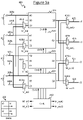
- FIG. 1 of the present document reproduces the schematic of an existing circuit 100 as disclosed previously in GB 2,553,010 (Nield et al). (This corresponds to FIG. 4 in Nield.)
- the circuit 100 is designed for use in a processing block of a processor such as a GPU (graphics processing unit).
- the circuit 100 of Nield comprises a plurality of parallel processing channels P, in this case four processing channels P 0 . . . P 3 .
- Each processing channel P 0 . . . P 3 comprises a respective logic unit, labelled 101 , 102 , 103 , 104 respectively.
- each of these may comprise a respective arithmetic logic unit (ALU).
- ALU arithmetic logic unit
- P 3 comprises a respective first input line and second input line: respective first and second input lines 105 a , 105 b of the first channel P 0 ; respective first and second input lines 106 a , 106 b of the second channel P 1 ; respective first and second input lines 107 a , 107 b of the third channel P 2 ; and respective first and second input lines 108 a , 108 b of the fourth channel P 3 .
- Each respective logic unit 101 . . . 104 also comprises at least a respective first and second input to the logic unit itself, and a respective output from the logic unit (i.e. the input and output terminals of the logic unit).
- the circuit 100 also comprises multiplexing circuitry 113 - 116 c .
- This comprises: a three-way multiplexer 113 of the first processing channel P 0 , a two-way multiplexer 114 a and three-way multiplexer 114 c of the second processing channel P 1 , a two-way multiplexer 115 a and three-way multiplexer 115 c of the third processing channel P 2 , and a four-way multiplexer 116 a and three-way multiplexer 116 c of the fourth processing channel P 3 .
- the first input line 105 a of the first processing channel P 0 is coupled to the first input of the first logic unit 101 .
- the three-way multiplexer 113 of the first processing channel P 0 is arranged to selectively couple the second input of the first logic unit 101 to any selected one of: the second input line 105 b of the first channel P 0 , the first input line 106 a of the second channel P 1 , or the first input line 107 a of the third channel P 2 .
- the two-way multiplexer 114 a of the second processing channel P 1 is arranged to selectively couple the first input of the second logic unit 102 to either selected one of: the first input line 106 a of the second channel P 1 , or the first input line 105 a of the first channel P 0 .
- the three-way multiplexer 114 c of the second processing channel P 1 is arranged to selectively couple the second input of the second logic unit 102 to any selected one of: the second input line 106 b of the second channel P 1 , the first input line 107 a of the third channel P 2 , or the first input line 108 a of the fourth channel P 3 .
- the two-way multiplexer 115 a of the third processing channel P 2 is arranged to selectively couple the first input of the third logic unit 103 to either selected one of: the first input line 107 a of the third channel P 2 , or the first input line 105 a of the first channel P 0 .
- the three-way multiplexer of the third processing channel P 2 is arranged to selectively couple the second input of the third logic unit 103 to any selected one of: the second input line 107 b of the third channel P 2 , the first input line 106 a of the second channel P 1 , or the first input line 108 a of the fourth channel P 3 .
- the four-way multiplexer 116 a of the fourth processing channel P 3 is arranged to selectively couple the first input of the fourth logic unit 104 to any selected one of: the first input line 108 a of the fourth channel P 3 , the first input line 105 a of the first channel P 0 , the first input line 106 a of the second channel P 1 , or the first input line 107 a of the third channel P 2 .
- the three-way multiplexer 116 c of the fourth processing channel P 3 is arranged to selectively couple the second input of the fourth logic unit 104 to any selected one of: the second input line 108 b of the fourth channel P 3 , the first input line 106 a of the second channel P 1 , or the first input line 107 a of the third channel P 2 .
- Each logic unit 101 . . . 104 is operable to perform one or more types of operation in response to one or more types of logic instruction being executed by the processor.
- the supported operations include at least a subtraction operation, and preferably also a multiply-accumulate (MAC) operation.
- MAC multiply-accumulate
- each logic unit 101 . . . 104 comprises at least three respective inputs: two respective multiplication inputs (multiplier and multiplicand inputs) and an addend input (also called the accumulator input).
- the first input of each logic unit as mentioned above is one of the respective multiplication inputs
- the second input mentioned above is the respective addend input.
- the two multiplication inputs of each logic unit are operable to receive two respective multiplication values, sometimes referred to as a multiplicand and multiplier.
- the addend input is operable to receive an addend value (the accumulator value).
- the logic unit determines a product of the two multiplication values and adds the addend to the product.
- Such a logic unit can also be used to perform a subtraction. Depending on implementation, this may be done for example by setting one of the multiplication inputs to ⁇ 1, or by switching the logic to an alternative mode in which it subtracts one of the multiplication inputs from the addend input (and ignores the other multiplication input) instead of performing the MAC.
- the multiplexers 113 - 116 c are simply set to couple the respective first and second input lines of their own respective processing channel P 0 . . . P 3 to the first and second inputs of the respective logic unit 101 . . . 104 of that channel. So the input lines 105 a , 105 b of the first channel P 0 are coupled to the inputs of the first logic unit 101 ; and the input lines 106 a , 106 b are coupled to the inputs of the second logic unit 102 ; etc.
- This mode may be used to enable each logic unit 101 . . .
- the multiplexers 113 - 116 c in the circuit 100 of FIG. 1 can be set to perform cross-over operations whereby the input line of one channel is routed to the logic unit of another. These operations comprise gradient operations for determining the difference between the values input on the input lines of different processing channels.
- FIG. 2 illustrates an example application of the circuit 100 of FIG. 1 (and of the circuit 400 of FIG. 4 , to be discussed in more detail shortly).
- FIG. 2 shows a 2 ⁇ 2 block of four adjacent pixels: a top-left pixel 201 TL, a top-right pixel 201 TR, a bottom-left pixel 201 BL and a bottom-right pixel 201 BR.
- Light here means a greater x coordinate and “left” a lesser x coordinate, whilst “top” means a lesser y coordinate and “bottom” means a greater y coordinate.
- the top pixels 201 TL & 201 TR are the top-most in the block, but not necessarily the top-most in the image or screen area as a whole; and similarly the right pixels 201 TR & 201 BR are the right-most in the block, but again not necessarily the right-most in the image or screen as a whole.
- the four pixels 201 TL, 201 TR, 201 BL, 201 BR are adjacent to one another, meaning having consecutive values of the x and/or y coordinates at whatever resolution pixels are being processed at in the operations in question.
- Each pixel 201 TL, 201 TR, 201 BL & 201 BR has a respective associated signal value s 0 , s 1 , s 2 , s 3 respectively.
- s 0 , s 1 , s 2 , s 3 respectively.
- each input signal could be an intensity of the pixel, or a value of a particular colour channel in a colour space such as RGB or YUV, or a shading or texture value, etc.
- the signals s 0 . . . s 3 typically all represent the same kind of quantity as one another (e.g. intensity or texture, etc.).
- the respective input signal s 0 . . . s 3 from each pixel 201 TL, 201 TR, 201 BL & 201 BR is associated with a different respective one of the parallel processing channels P 0 . . . P 3 .
- Each signal s 0 . . . s 3 may be input on one of the input lines (e.g. the respective first input line 105 a , 106 a , 107 a , 108 a ) of a different respective one of the processing channels P 0 . . . P 3 .
- each logic unit 101 . . . 104 operates on the input signal value s 0 . . .
- the input signals s 0 . . . s 3 could equally be signals representing image fragments.
- an application outputs a 3D model defined in terms of a plurality of facets, e.g. triangular facets. In successive pipeline stages, these may be translated, rotated, and have lighting effects applied. In another successive stage, the facets are projected from 3D space to the 2D space of the screen area, and some facets that fall outside the screen area may be culled. In a further pipeline stage, the 2D projections of the facets are rasterized, meaning to map them to onto a pixel grid.
- the points on the pixel grid may be referred to as image fragments.
- image fragments There is a one-to-one mapping between fragments and pixels in the x-y plane.
- some of the fragments of different facets may be behind one another in the z direction. Therefore another pipeline stage will perform a hidden surface removal (also referred to as a z test or depth test), to determine which fragments are behind others in order to cull these.
- the remaining points after the hidden surface removal are the actual pixels to be lit up on the screen.
- Other pipeline stages such as texturing and shading may also be performed on fragments or pixels, depending on the order of the pipeline stages.
- the graphics operations disclosed anywhere herein may be performed on fragments or pixels, depending on implementation, and the signals s 0 . . .
- s 3 described anywhere herein may represent pixel values or values associated with fragments.
- pixel values or values associated with fragments For convenience embodiments may be described in terms of pixels by way of example, but it will be appreciated that this is not limiting and any of the disclosed embodiments could equally be applied to fragments. Note also that the stages in a graphics pipeline can be implemented in different orders.
- FIG. 3 a shows how the circuit 100 of FIG. 1 can be used to perform a coarse gradient operation in the x direction, e.g. to execute a coarse ds/dx instruction from the processor's instruction set.
- This instruction may be referred to herein as DSX, but this is not intended to limit the scope of the disclosure to any particular instruction of any particular instruction set.
- the multiplexing circuitry 113 - 116 c is set so as to route s 0 to the first input of each of the logic units 101 . . . 104 , and to route s 1 to the second input of each logic unit 101 . . . 104 .
- each of the logic units 101 . . . 104 performs s 1 ⁇ s 0 and outputs the result of this as the gradient of the respective pixel (or fragment) 201 TL, 201 TR, 201 BL, 201 BR associated with the respective processing channel P 0 . . . P 3 .
- FIG. 3 b shows how the circuit 100 of FIG. 1 can be used to perform a coarse gradient operation in the y direction, e.g. to execute a coarse ds/dy instruction from the processor's instruction set.
- This instruction may be referred to herein as DSY, but this is not intended to limit the scope of the disclosure to any particular instruction of any particular instruction set.
- the multiplexing circuitry 113 - 116 c is set so as to route s 0 to the first input of each of the logic units 101 . . . 104 , and to route s 2 to the second input of each logic unit 101 . . . 104 .
- each of the logic units 101 . . . 104 performs s 2 ⁇ s 0 . This again makes the approximation that the gradient at each pixel is approximately the same.
- FIG. 3 c shows how the circuit 100 of FIG. 1 can be used to perform a fine gradient operation in the x direction, e.g. to execute a fine ds/dx instruction from the processor's instruction set.
- This instruction may be referred to herein as DSDX, but this is not intended to limit the scope of the disclosure to any particular instruction of any particular instruction set.
- the multiplexing circuitry 113 - 116 c is set so as to route s 0 to the first input of each of the first and second logic units 101 , 102 ; and to route s 2 to the first input of each of the third and fourth logic units 103 , 104 .
- the multiplexing circuitry 113 - 116 c also routes s 1 to the second input of each of the first and second logic units 101 , 102 ; and routes s 3 to the second input of each of the third and fourth logic units 103 , 104 .
- Each logic unit 101 . . . 104 is set to a state where it performs a subtraction of its respective first input from its second input (e.g. as above).
- each of the first and second logic units 101 , 102 performs s 1 ⁇ s 0 and outputs the result of this as the gradient of its respective pixel (or fragment) 201 TL, 201 TR respectively.
- each of the third and fourth logic units performs s 3 ⁇ s 2 and outputs the result of this as the gradient of its respective pixel (or fragment) 201 BL, 201 BR respectively.
- the gradient in the x direction is modelled as being pseudo-constant in the x direction, i.e. approximately the same over a small distance from one pixel (or fragment) to the next in the x direction.
- FIG. 3 d shows how the circuit 100 of FIG. 1 can be used to perform a fine gradient operation in the y direction, e.g. to execute a fine ds/dy instruction from the processor's instruction set.
- This instruction may be referred to herein as DSDY, but this is not intended to limit the scope of the disclosure to any particular instruction of any particular instruction set.
- the multiplexing circuitry 113 - 116 c is set so as to route s 0 to the first input of each of the first and third logic units 101 , 103 ; and to route s 1 to the first input of each of the second and fourth logic units 102 , 104 .
- the multiplexing circuitry 113 - 116 c also routes s 2 to the second input of each of the first and third logic units 101 , 103 ; and routes s 3 to the second input of each of the second and fourth logic units 102 , 104 .
- Each logic unit 101 . . . 104 is again set to a state where it performs a subtraction of its respective first input from its second input.
- each of the first and third logic units 101 , 103 performs s 2 ⁇ s 0 and outputs the result of this as the gradient of its respective pixel (or fragment) 201 TL, 201 BL respectively.
- each of the second and fourth logic units 102 , 104 performs s 3 ⁇ s 1 and outputs the result of this as the gradient of its respective pixel (or fragment) 201 TR, 201 BR respectively.
- a gradient value of each respective pixel is required to be output by each processing channel in association with the respective pixel.
- the gradient of, or associated with, a given pixel is a short-hand used herein to mean the gradient of the signal s at the x and y coordinates of the respective pixel. If the gradient is calculated over a step of 1 pixel in the x or y direction, then dx or dy is 1 in magnitude and determining the gradient amounts to determining the difference in the positive x or y direction.
- both of the first and second logic units 101 , 102 each perform a duplicate instance of the same operation s 1 ⁇ s 0 .
- both of the third and fourth logic units each perform a duplicate instance of the same operation s 3 ⁇ s 2 .
- a similar observation may be made in FIG. 3 d mutatis mutandis in the y direction.
- FIG. 4 discloses and example of a circuit 400 which avoids this duplication by applying some of the multiplexing on the output lines of the processing channels P 0 . . . P 3 rather than just on the input lines.
- the circuit 400 comprises a plurality of parallel processing channels P, in this example four processing channels P 0 . . . P 3 .
- Each processing channel P 0 . . . P 3 comprises a respective logic unit, again labelled 101 , 102 , 103 , 104 respectively.
- each of these may comprise a respective arithmetic logic unit (ALU), such as an integer arithmetic logic unit or a floating point arithmetic logic unit.
- ALU arithmetic logic unit
- P 3 comprises a respective first input line and second input line: respective first and second input lines 105 a , 105 b of the first channel P 0 ; respective first and second input lines 106 a , 106 b of the second channel P 1 ; respective first and second input lines 107 a , 107 b of the third channel P 2 ; and respective first and second input lines 108 a , 108 b of the fourth channel P 3 .
- Each processing channel P 0 . . . P 3 also comprises a respective output line 425 , 426 , 427 , 428 .
- Each respective logic unit 101 . . . 104 also comprises at least a respective first input A and second input C to the logic unit itself, and a respective output Q from the logic unit (i.e. the input and output terminals of the logic unit).
- the first input line of each processing channel P 0 . . . P 3 is coupled to the respective first input A 0 . . . A 3 of the respective logic unit 101 . . . 104 . That is, the first input line 105 a of the first processing channel P 0 is coupled to the first input A 0 of the first logic unit 101 .
- the first input line 106 a of the second processing channel P 1 is coupled to the first input A 1 of the second logic unit 102 .
- the first input line 107 a of the third processing channel P 2 is coupled to the first input A 2 of the third logic unit 103 .
- the first input line 108 a of the fourth processing channel P 3 is coupled to the first input A 3 of the fourth logic unit 104 .
- the circuit 400 further comprises multiplexing circuitry 410 i - iv , 420 i - iv for selectively coupling input lines to the inputs of the logic units 101 . . . 104 , and selectively output lines of the processing channels to the outputs of the logic units. This enables input lines of each processing channel P 0 . . . P 3 to be selectively routed to inputs of different ones of the logic units 101 , 102 , 103 , 104 in certain combinations.
- the input multiplexers comprise a first input multiplexer 410 i , a second input multiplexer 410 ii , a third input multiplexer 410 iii , and a fourth input multiplexer 410 iv .
- the output multiplexers comprise a first output multiplexer 420 i , a second output multiplexer 420 ii , a third output multiplexer 420 iii , and a fourth output multiplexer 420 iv .
- the circuit 400 further comprises control circuitry 450 , coupled to a respective control input of each of the logic units; and to a respective control inputs of each of the multiplexers 410 i - iv , 420 i - iv .
- the control circuitry 450 is arranged to supply a respective control signal M_in 0 . . . M_in 3 and M_out 0 . . . M_out 3 to each of the input and output multiplexers 410 i . . . 410 iv and 420 i . . . 420 iv respectively, in order to switch the multiplexers.
- the control circuitry 450 is also arranged to supply a respective control signal Ctrl 0 . . . Ctrl 3 to each of the logic units (e.g. ALUs) 101 . . . 104 respectively, in order to control the logic units 101 . . . 104 themselves such as to switch mode (e.g.
- each of Ctrl 0 . . . Ctrl 3 could represent a plurality of individual constituent signals for different control purposes, such as a respective mode signal for controlling the mode and a respective power state signal for switching the unit between the idle and operative state).
- the reduced-power state could be created, for example, by setting the data inputs A, B, C of the respective unit to a static value such as 0.
- the first input multiplexer 410 i is arranged to selectively couple the second input C 0 of the first logic unit 101 to either selected one of: the second input line 105 b of the first processing channel P 0 , or the first input line 106 a of the second processing channel P 1 .
- the selection is made via a respective control signal M_in 0 received from the control circuitry 450 .
- the second input multiplexer 410 ii is arranged to selectively couple the second input C 2 of the third logic unit 103 to either selected one of: the second input line 107 b of the third processing channel P 2 , or the first input line 105 a of the first processing channel P 0 .
- the selection is made via a respective control signal M_in 2 received from the control circuitry 450 .
- the third input multiplexer 410 iii is arranged to selectively couple the second input C 1 of the second logic unit 102 to either selected one of: the second input line 106 b of the second processing channel P 1 , or the first input line 108 a of the fourth processing channel P 3 .
- the selection is made under control of a respective control signal M_in 1 received from the control circuitry.
- the selection is made via a respective control signal M_in 1 received from the control circuitry 450 .
- the fourth input multiplexer 410 iv is arranged to selectively couple the second input C 3 of the fourth logic unit 104 to either selected one of: the second input line 108 b of the fourth processing channel P 3 , or the first input line 107 a of the third processing channel P 2 .
- the selection is made via a respective control signal M_in 3 received from the control circuitry 450 .
- the first output multiplexer 420 i is arranged to selectively couple the output line 426 of the second processing channel P 1 to either selected one of: the output Q 1 of the second processing unit 102 , or the output Q 0 of the first logic unit 101 .
- the selection is made via a respective control signal M_out 1 received from the control circuitry 450 .
- the second output multiplexer 420 ii is arranged to selectively couple the output line 425 of the first processing channel P 0 to either selected one of: the output Q 0 of the first logic unit 101 , or the output Q 2 of the third logic unit 103 .
- the selection is made by a respective control signal M_out 0 received from the control circuitry 450 .
- the third output multiplexer 420 iii is arranged to selectively couple the output line 428 of the fourth processing channel P 3 to either selected one of: the output Q 3 of the fourth logic unit 104 , or the output Q 1 of the second logic unit 102 .
- the selection is made by a respective control signal M_out 3 received from the control circuitry 450 .
- the fourth output multiplexer 420 iv is arranged to selectively couple the output line 427 of the third processing channel P 2 to either selected one of: the output Q 2 of the third logic unit 103 , or the output Q 3 of the fourth logic unit 104 .
- the selection is made by a respective control signal M_out 3 received from the control circuitry 450 .
- a multiplexer selectively couples one point in a circuit to either (or any) selected one of two (or more) other points in the circuit, this means it selects to couple to only one of those other points and not both (or not more than one).
- the term “coupled” herein means operatively coupled, which covers the possibility of being directly connected (with only a conductor in between) or coupling via one or more intermediate components. In embodiments the term “coupled” anywhere herein may be replaced with “connected” or “directly connected”.
- Each logic unit 101 . . . 104 is operable to perform one or more types of operation in response to one or more types of instruction being executed by the processor (e.g. integer or floating point instructions).
- the supported operations include at least a subtraction operation, and in embodiments also a multiply-accumulate (MAC) operation.
- MAC multiply-accumulate
- each logic unit 101 . . . 104 comprises at least three respective inputs: two respective multiplication inputs A, B (multiplier and multiplicand inputs); and an addend input C (also called the accumulator input).
- the “first” input of each logic unit is one of the respective multiplication inputs (A in the illustrated example, though it could be B in other implementations); and the “second” input is the respective addend input C.
- the two multiplication inputs A, B of each logic unit are operable to receive two respective multiplication values, sometimes referred to as a multiplicand and multiplier.
- the addend input C is operable to receive an addend value (the accumulator value).
- FMA fused-multiply add
- control circuitry 450 may be coupled to a respective control input of each logic unit 101 . . . 104 , arranged to receive a respective control signal Ctrl 0 . . . Ctrl 3 from the control circuitry 450 .
- This enables the control circuitry 450 to control the ALUs 101 . . . 104 themselves, in addition to being able to control the multiplexing circuitry 410 , 420 via signals M_in 0 . . . 3 and M_out 0 . . . 3 .
- this may be used for the control circuitry 450 to control the logic units 101 . . . 104 to switch between different types of logic operation, e.g. MAC and subtract; and/or to switch unused ones of the logic units 101 . . . 104 to a reduced power state.
- the first input line 105 a , 106 a , 107 a , 108 a of each processing channel P 0 . . . P 3 is arranged to receive a respective input signal s 0 . . . s 3 .
- each of these signals may be the signal associated with a different respective pixel or image fragment 201 TL, 201 TR, 201 BL, 201 BR in a 2 ⁇ 2 block of adjacent pixels or fragments, as discussed previously with respective to FIG. 2 .
- each signal may represent an intensity, colour channel value, texture or shading value of a different respective one of the pixels (or fragments) in the block 200 .
- the second input line 105 b , 106 b , 107 b , 108 b of each processing channel P 0 . . . P 3 may be arranged to receive another value associated with the respective signal, e.g. an accumulator.
- the output line 425 , 426 , 427 , 428 of each processing channel P 0 . . . P 3 is arranged to supply a respective result r 0 . . . r 3 as an output of the respective processing channel.
- the respective result r 0 . . . r 3 output by each channel P 0 . . . P 3 is associated with a different respective one of the pixels (or fragments) 201 TL, 201 TR, 201 BL, 201 BR in the block.
- the control circuitry 450 sets the input multiplexers 410 i - iv to couple the respective first and second input lines of each processing channel P 0 . . . P 3 to the respective first and second inputs A, C of the respective logic unit 101 . . . 104 of that same channel.
- the output multiplexers are simply set to couple the respective output line of each channel P 0 . . . P 3 to the output Q 0 . . . Q 3 of the respective logic unit 101 . . . 104 of that channel.
- the input lines 105 a , 105 b of the first channel P 0 are coupled to the inputs A 0 , C 0 of the first logic unit 101 ; and the input lines 106 a , 106 b are coupled to the inputs A 1 , C 1 of the second logic unit 102 ; the input lines 107 a , 107 b of the third channel P 2 are coupled to the inputs A 2 , C 2 of the third logic unit 103 ; and the input lines 108 a , 108 b are coupled to the inputs A 3 , C 3 of the fourth logic unit 104 .
- the output line 425 of the first channel P 0 is coupled to the output Q 0 of the first logic unit 101
- the output line 426 of the second channel P 1 is coupled to the output Q 1 of the second logic unit 102
- the output line 427 of the third channel P 2 is coupled to the output Q 2 of the third logic unit 103
- the output line 428 of the fourth channel is coupled to the output Q 3 of the fourth logic unit 104 .
- the multiplexers are set into this configuration by the control circuitry 450 , which sets the input and output multiplexers 410 i - iv , 420 i - iv to the relevant settings via their respective control inputs M_in 0 . . . M_in 3 , M_out 0 . . . M_out 3 .
- this mode may be used to enable each logic unit 101 . . . 104 to perform a multiply-accumulate (MAC) operation on the respective values received on the respective first and second inputs lines of its own respective channel P 0 . . . P 3 (also using the respective other multiplication input B to each logic unit).
- the control circuitry 450 may control each of the logic units 101 . . . 104 , via the control signal Ctrl 0 . . . 3 supplied to their respective control inputs, to enter a state in which they perform a MAC operation on their respective inputs A, B, C and output the result at their respective output Q.
- control circuitry 450 may be configured to operate the circuit 400 in the first mode responsive to the execution of an instance of a MAC instruction, being a dedicated machine code instruction of the processor instruction set.
- FIG. 5 a illustrates how the circuit of FIG. 4 can be operated in a second, alternative mode of operation to determine differences between the input signals s 0 . . . s 3 of different processing channels P 0 . . . P 3 . In embodiments, this may be used to perform a fine gradient operation in the x direction, such as to execute the DSDX instruction.
- the bold lines in FIG. 5 a show where the signals are routed by the multiplexers.
- the control circuitry 450 controls the first input multiplexer 410 i (via M_in 0 ) to couple the second input C 0 of the first logic unit 101 to the first input line 106 a of the second processing channel P 1 , in order to receive s 1 .
- the control circuitry 450 also controls the fourth input multiplexer 410 iv (via M_in 3 ) to couple the second input C 3 of the fourth logic unit 104 to the first input line 107 a of the third processing channel P 2 , in order to receive s 2 .
- the state of the second and third multiplexers 410 ii , 410 iii does not matter in this mode.
- the control circuitry 450 controls the first output multiplexer 420 i (via M_out 1 ) to couple the output line 426 of the second processing channel P 1 to the output Q 0 of the first logic unit 101 .
- the control circuitry 450 also controls the second output multiplexer 420 ii (via M_out 0 ) to couple the output line 425 of the first processing channel P 0 to the output Q 0 of the first logic unit 101 .
- the control circuitry 450 also controls the third output multiplexer 420 iii (via M_out 3 ) to couple the output line 428 of the fourth processing channel P 3 to the output Q 3 of the fourth logic unit 104 . It also controls the fourth output multiplexer 420 iv (via M_out 2 ) to couple the output line 427 of the third processing channel P 2 to the output Q 3 of the fourth logic unit 104 .
- the signal s 1 from the first input line 106 a of the second processing channel P 1 is routed to the logic unit 101 of the first processing channel P 0 ; and the signal s 2 from the first input line 107 a of the third processing channel P 2 is routed to the logic unit 104 of the fourth processing channel P 3 .
- the output Q 0 of the first logic unit 101 in the first processing channel P 0 is routed to the output lines 425 , 426 supplying the result r 0 , r 1 of both the first and second channels P 0 , P 1 (e.g. corresponding to both the top row pixels 201 TL, 201 TR).
- the output Q 3 of the fourth logic unit 104 in the fourth processing channel P 3 is routed to the output lines 427 , 428 supplying the results r 2 , r 3 of both the third and fourth channels P 2 , P 3 (e.g. corresponding to both the bottom row pixels 201 BL, 201 BR)
- the control circuitry 450 also controls the first logic unit 101 to switch to a state in which it performs a subtraction of its first input A 0 from its second input C 0 .
- This may be done by controlling the logic unit 101 , via the signal Ctrl 0 supplied to its respective control input, to switch to a mode in which it ignores the other multiplication input (e.g. multiplicand) B and negates the first input A in order to subtract A from C.
- the circuit 400 of FIG. 4 thus exploits the ability of the logic units to perform either C ⁇ A or A ⁇ C.
- the first logic unit 101 performs s 1 ⁇ s 0 , and the output multiplexing circuitry 420 i , 420 ii routes the output Q 0 to the output lines 425 , 426 of both the first and second processing channels P 0 , P 1 to deliver the respective results r 0 , r 1 of both channels.
- the fourth logic unit 104 performs s 3 ⁇ s 1 , and the output multiplexing circuitry 420 iii , 420 iv routes the output Q 3 to the output lines 427 , 428 of both the third and fourth processing channels P 2 , P 3 to deliver the respective results r 2 , r 3 of both these channels.
- the second and third logic units 102 , 103 are not used in the second mode.
- the circuit 400 of FIG. 4 only requires two two-way multiplexers per channel (one two-way input multiplexer per channel and one two-way output multiplexer per channel). This reduces the amount of circuitry compared to the circuit 100 of FIG. 1 , where each of the second to fourth channels P 1 . . . P 3 requires a two-way multiplexer on one input and at least a three-way multiplexer on the other. Note that a three-way multiplexer is basically just formed of two two-way multiplexers.
- control circuitry 450 is configured to control the second and third logic units 102 , 103 (e.g. via Ctrl 1 & Ctrl 2 respectively) to enter a low power state when the circuit 400 is in the second mode. In other words they are deactivated, into a state where they perform no logic operation, in order to consume less power than if performing a logic operation.
- circuit of FIG. 400 is not configured to be able to perform the coarse gradient operation DSX or DSY. This saves the need for the four-way multiplexer 116 c in the fourth channel P 3 .
- the second mode may be used to determine the gradient in the x direction associated with each of the pixels (or fragments) 201 . I.e. the approximate gradient of the signal s in the x direction at the point of each of the pixels (or fragments) in the 2 ⁇ 2 block 200 .
- control circuitry 450 may be configured to operate the circuit 400 in the second mode in order to execute an instance of an x-direction gradient instruction, being a dedicated machine code instruction of the processor instruction set. E.g. this may be the DSDX instruction.
- FIG. 5 b illustrates how the circuit of FIG. 4 can be operated in a third, further alternative mode operation. In embodiments, this may be used to perform a fine gradient operation in the y direction, such as to execute the DSDY instruction.
- the bold lines in FIG. 5 b again show where the signals are routed by the multiplexers in this particular mode.
- the control circuitry 450 controls the third input multiplexer 410 iii (via M_in 1 ) to couple the second input C 1 of the second logic unit 102 to the first input line 108 a of the fourth processing channel P 0 , in order to receive s 3 .
- the control circuitry 450 also controls the second input multiplexer 410 ii (via M_in 2 ) to couple the second input C 2 of the third logic unit 103 to the first input line 105 a of the first processing channel P 0 , in order to receive s 0 .
- the state of the first and fourth multiplexers 410 i , 410 iv does not matter in the third mode.
- the control circuitry 450 controls the first output multiplexer 420 i (via M_out 1 ) to couple the output line 426 of the second processing channel P 1 to the output Q 1 of the second logic unit 102 .
- the control circuitry 450 also controls the second output multiplexer 420 ii (via M_out 0 ) to couple the output line 425 of the first processing channel P 0 to the output Q 2 of the third logic unit 103 .
- the control circuitry 450 also controls the third output multiplexer 410 iii (via M_out 3 ) to couple the output line 428 of the fourth processing channel P 3 to the output Q 1 of the second logic unit 102 . It also controls the fourth output multiplexer 420 iv (via M_out 2 ) to couple the output line 427 of the third processing channel P 2 to the output Q 2 of the third logic unit 103 .
- the signal s 0 from the first input line 105 a of the first processing channel P 0 is routed to the logic unit 103 of the third processing channel P 2 ; and the signal s 3 from the first input line 108 a of the fourth processing channel P 3 is routed to the logic unit 102 of the second processing channel P 1 .
- the output Q 1 of the second logic unit 102 in the second processing channel P 1 is routed to the output lines 426 , 428 supplying the result r 1 , r 3 of both the second and fourth channels P 1 , P 3 (e.g. corresponding to both the right-hand pixels 201 TR, 201 BR).
- the output Q 2 of the third logic unit 103 in the third processing channel P 2 is routed to the output lines 425 , 427 supplying the results r 0 , r 2 of both the first and third channels P 0 , P 2 (e.g. corresponding to both left-hand pixels 201 TL, 201 BL).
- control circuitry 450 also controls the second logic unit 102 to switch to a state in which it performs a subtraction of its first input A from its second input C. This may be done by controlling the logic unit 102 , via the signal Ctrl 1 supplied its respective control input, to switch to a mode in which it ignores the other multiplication input (e.g. multiplicand) B and negates the first input A in order to subtract A form C. Alternatively for example, the same result could be achieved by setting B to ⁇ 1 and leaving the logic unit 102 in the MAC mode.
- multiplication input e.g. multiplicand
- the control circuitry 450 also controls the third logic unit 103 to switch to a state in which it performs a subtraction of its second input C 2 from its first input A 2 . This may be done by controlling the logic unit 103 (via Ctrl 2 ) to a mode in which it ignores the other multiplication input (e.g. multiplicand) B, and negates the second input C in order to subtract C from A. Alternatively the same result could be achieved by setting B to ⁇ 1, performing a MAC, and negating the output Q.
- the third logic unit 103 controls the third logic unit 103 to switch to a state in which it performs a subtraction of its second input C 2 from its first input A 2 . This may be done by controlling the logic unit 103 (via Ctrl 2 ) to a mode in which it ignores the other multiplication input (e.g. multiplicand) B, and negates the second input C in order to subtract C from A. Alternatively the same result could be achieved by setting B to ⁇ 1, performing a
- the second logic unit 102 performs s 3 ⁇ s 1 , and the output multiplexing circuitry 420 i , 420 iii routes the output Q 1 to the output lines 426 , 428 of both the second and fourth processing channels P 1 , P 3 to deliver the respective results r 1 , r 3 of both channels.
- the third logic unit 103 performs s 2 ⁇ s 0 , and the output multiplexing circuitry 420 ii , 420 iv routes the output Q 2 to the output lines 425 , 427 of both the first and third processing channels P 0 , P 2 to deliver the respective results r 0 , r 2 of both these channels.
- the first and fourth logic units 101 , 104 are not used in the third mode.
- control circuitry 450 is configured to control the first and fourth logic units 101 , 104 to enter a an idle, low-power state when the circuit 400 is in the third mode. I.e. they are set into a state where they perform no operation, in order to consume less power than if performing an operation. This could be done by completely removing power (i.e. voltage), but such an approach is not typically done at this scale because it requires a lot of logic to safely save the state and shut down. At the scale of circuitry in question, instead therefore clock-gating may be used, or another way of keeping the signals stable for one or more clock cycles. This saves power because it is changing signals that consume most of the power in a logic circuit such as this.
- the third mode may be used to determine the gradient in the y direction associated with each of the pixels (or fragments) 201 . I.e. the approximate gradient of the signal s in the y direction at the point of each of the pixels (or fragments) in the 2 ⁇ 2 block 200 .
- control circuitry 450 may be configured to operate the circuit 400 in the third mode in order to execute an instance of a y-direction gradient instruction, being a dedicated machine code instruction of the processor instruction set. E.g. this may be the DSDY instruction.
- FIG. 6 a illustrates how a variant of the circuit of FIG. 4 can be operated in a fourth mode of operation to perform a swap operation in the x direction, e.g. to execute a SWPX instruction.
- the input signal s 0 input on the first input line 105 a of the first processing channel P 0 is swapped over to the output line 426 of the second processing channel P 1
- the input signal s 1 input on the first input line 106 a of the second processing channel P 1 is swapped over to the output line 425 of the first processing channel P 0 ; and similarly for s 2 and s 3 .
- FIG. 6 b illustrates how a variant of the circuit of FIG. 4 can be operated in a fifth mode of operation to perform a swap operation in the y direction, e.g. to execute a SWPY instruction.
- the input signal s 0 input on the first input line 105 a of the first processing channel P 0 is swapped over to the output line 427 of the third processing channel P 2
- the input signal s 2 input on the first input line 107 a of the third processing channel P 2 is swapped over to the output line 425 of the first processing channel P 0 ; and similarly for s 2 and s 4 .
- the swap re-uses the multiplexers that are already available for the gradient instructions.
- the swap works by using a separate channel within one of the logic units.
- the additional output needed can be created cheaply almost completely out of the critical path making it virtually free (because it can be known very early which signals are going to be output output).
- the ability to perform a swap gives an additional advantage of structuring the logic units and associated multiplexing circuity in the manner disclosed.
- Swap x and swap y operations require moving two pieces of data through (some of) the logic units 101 . . . 104 .
- Swapping between two logic unit instances is achieved by sending a value from one instance to the other on the input side input, and the other instance sending its own input back to the one instance on the output side.
- each of the logic units 101 . . . 104 may comprise two independent output terminals, O 0 . . . O 3 and Q 0 . . . Q 3 , respectively.
- Implementing a gradient mode in this variant can be achieved by making Q and O hold the same value, in which case the circuit shown in FIGS. 6 a and 6 b reduces to that of FIG. 4 .
- reference to a given output Q may in fact, in some embodiments, refer to the logical output of the respective logic unit and not necessarily a single direct physical output connection.
- Q and O of a given logic unit are set independently of one another and can take different values.
- the multiplexors 420 select between Q of their own logic unit and O of the other instance.
- s 1 is sent from 102 to 101 , which then outputs s 0 via O 0 and s 1 via Q 0 .
- the multiplexer 420 ii sends Q 0 to r 0 .
- the multiplexer 420 i sends O 0 to r 1 .
- 102 can be switch off during this operation.
- the behaviour of 103 and 104 is similar and the SWPY operation is symmetrical.
- the multiplexing circuitry routes the signal s 0 input on the first input line 105 a of the first processing channel P 0 to the output line r 1 of the second processing channel P 1 via the first input A 0 and first independent output O 0 of the first logic unit 101 , and routes the signal s 1 input on the first input line 106 a of the second processing channel P 1 to the output line r 0 of the first processing channel P 0 via the second input C 0 and second independent output Q 0 of the first logic unit 101 .
- the multiplexing circuitry routes the signal s 2 input on the first input line 107 a of the third processing channel P 2 to the output line r 0 of the first processing channel P 0 via the first input A 2 and first independent output O 2 of the third logic unit 103 , and routes the signal s 0 input on the first input line 105 a of the first processing channel P 0 to the output line r 2 of the third processing channel P 3 via the second input C 2 and second independent output Q 2 of the third logic unit 103 .
- the first and fourth logic units 101 , 104 do not need to be used.
- the two respective independent outputs O, Q of each logic unit are simply held at the same value as one other, thereby in effect forming the same output as shown in FIGS. 4 and 5 a - b .
- O 0 and Q 0 are held at the same value as one another, whilst O 1 and Q 1 are held at the same value as one another, and O 2 and Q 2 are held at the same value as one another, and O 3 and Q 3 are held at the same value as one another.
- FIG. 7 illustrates an example method in accordance with embodiments disclosed herein.
- the processor fetches a machine code instruction from memory.
- the processor decodes the instruction to determine what type of instruction it is based on its opcode, and to supply the relevant input data specified by the instruction's operand(s) on the input lines of the circuit 400 in the execution stage. If the instruction is determined to be of a first type, e.g. a multiply-accumulate (MAC) instruction, the method branches to step S 715 where the control circuitry 450 sets the circuit 400 into the first mode. If the instruction is determined to be of a second type, e.g. a DSDX instruction, the method branches to step S 720 where the control circuitry 450 sets the circuit 400 to the second mode.
- MAC multiply-accumulate
- the method branches to step 725 where the control circuitry 450 sets the circuit 400 to the third mode.
- the instruction is determined to be of a fourth type, e.g. SWPX
- the method branches to step 730 where the control circuitry 450 sets the circuit 400 to the fourth mode.
- the instruction is determined to be of a fifth type, e.g. SWPY
- the method branches to step 735 where the control circuitry 450 sets the circuit to the fifth mode.
- step 740 the circuit 400 executes the instruction in the selected mode.
- FIG. 12 gives a high level schematic representation of the configuration of four logic units (e.g. ALUs) as shown in FIGS. 4, 5 a - b and 6 a - b .
- a different one of the logic units (e.g. ALUs) 101 . . . 104 lies in each corner of the illustration, with its inputs on the inside and its outputs on the outside.
- FIG. 12 A further possible mode of operation is revealed by studying FIG. 12 .
- the DSDX (or SWPX) instruction is computed by the top-left and bottom-right ALUs, while the DSDY (or SWPY) instruction is computed by the top-right and bottom-left ALUs.
- the DSDX and DSDY could be computed in parallel.
- a ds/dx gradient operation and a ds/dy gradient operation could be performed in parallel, i.e. at the same time.
- This configuration also enables 4-way clockwise or counter-clockwise swaps.
- the illustrated configuration cannot simultaneously swap top-left with top-right, bottom-left with bottom-right, top-left with bottom-left, and top-right with bottom right (i.e. both swap x and swap y simultaneously). In fact it can swap them, but as it has only a single output line per channel, it can only output one of the swaps at a time.
- the circuit could be extended again with an additional output line to enable a swap x and swap y to be performed on parallel (as opposed to just x direction swaps or y-direction swaps, or just clockwise or counter clockwise swaps).
- the logic units 101 . . . 104 are ALUs or floating point units capable of performing MAC operations in the first mode.
- the principles of crossing over the data lines of the channels at the input and output of the logic units could also be employed in other arrangements where the processing channels comprise other types of logic unit.
- the logic units could perform different types of operation in the first mode than in the second mode (as described above); or alternatively they could perform the same type of operation in the first and second modes, but on different combinations of input data. For instance in the first mode a given processing channel may determine the difference between its own two respective inputs; whereas in the second mode it may determine the difference between the crossed-over input lines.
- FIG. 10 shows the simplest case of a circuit 400 ′ with only the first and second channels P 0 , P 1 ; e.g. for processing a 2 ⁇ 1 block of pixels 200 ′.
- the circuit 400 ′ can be used to perform parallel operations (e.g. parallel MACs) using the respective logic unit 101 , 102 of each channel P 0 , P 1 to operate on only the signals received on its own respective input lines.
- the logic unit 101 in the first channel P 0 is used to compute s 1 ⁇ s 0 and output the result for both channels P 0 , P 1 .
- the logic unit 102 in the second channel P 1 may be set to an idle, low-power state when the circuit is in the second mode (e.g. by powering down, or more preferably by clock-gating or setting inputs to a static value, as discussed previously).
- FIG. 11 shows another variant 400 ′′ of the circuit, this time having with three channels: P 0 , P 1 , P 2 .
- This can be used either to perform three parallel operations in the first mode (e.g. three parallel MACs), or to perform ds/dx between s 1 and s 0 in a first mode, or ds/dy between s 2 and s 0 in the third mode. For instance this could be used to process an L-shaped block of three pixels 200 ′′.
- circuits of the present disclosure could be used in any application that involves processing signals in parallel where, at some times, it desired to have each processing channel operate only on its own respective inputs, and at other times it is desired to determine a gradient or difference between the signals associated with different channels, or even more generally to operate on inputs of different channels.
- FIG. 8 shows a computer system in which any of the circuits described herein may be implemented.
- the computer system comprises a central processing unit (CPU) 802 , a graphics processing unit (GPU) 804 , a memory 806 , and one or more other devices 814 such as a display 816 , speakers 818 and/or a camera 819 .
- the GPU 804 may be arranged as an accelerator processor and the CPU 802 may be arranged as a host of the GPU.
- the memory 806 comprises one or more memory units employing one or more volatile and/or non-volatile memory media, e.g. a magnetic medium such as a hard disk; or an electronic medium such as a ROM, EEPROM, flash memory, (SSD), etc.
- a processing block 810 which comprises the above-described circuit 400 is implemented in the GPU 804 .
- the processing block 810 may be implemented in the CPU 802 or another form processor (not shown) such as a digital signal processor, neural network accelerator processor, crypto processor, etc., or any other form of application specific or general purpose processor.
- a host (CPU) and accelerator processor e.g. GPU
- the processor in which the processing block 810 is implemented may be arranged in a stand-alone processor, or in another relationship within a multi-processor system.
- the components of the computer system are arranged to be able to communicate with each other via a communications bus 820 or other such interconnect.
- the processor in which the processing block 810 is implemented e.g. the GPU 804 , is arranged to fetch instructions from memory 806 and pass them to the processing block 810 to be decoded and executed.
- the processing block 810 comprises one or more of types of logic unit for performing logical operations specified by the fetched instructions.
- This processing block 810 includes the circuit 400 described above, including the processing channels comprising the logic units (e.g. ALUs) 101 - 104 , arranged to execute logic instructions (e.g. arithmetic or floating point instructions such as MACs, gradient instructions and swap instructions).
- the operations may be performed on values held in registers of a register file (not shown) implemented on the same processor as the processing block 810 , in which case the processing block 810 further comprises a load-store unit for loading values from memory 806 into the register file and storing values from the register file back to memory in response to load and sore instructions respectively.
- the data may be stored in the same memory unit as the instructions or a different memory unit of the overall memory 806 of the processor.
- the logic unit(s) and load-store unit may be pipelined with respect to one another.
- FIGS. 4-6 are shown as comprising a number of functional blocks. This is schematic only and is not intended to define a strict division between different logic elements of such entities. Each functional block may be provided in any suitable manner.
- the circuits described herein may be embodied in hardware on an integrated circuit.
- the circuits described herein may be configured to perform any of the methods described herein.
- any of the functions, methods, techniques or components described above can be implemented in software, firmware, hardware (e.g., fixed logic circuitry), or any combination thereof.
- the terms “module,” “functionality,” “component”, “element”, “unit”, “block” and “logic” may be used herein to generally represent software, firmware, hardware, or any combination thereof.
- the module, functionality, component, element, unit, block or logic represents program code that performs the specified tasks when executed on a processor.
- a computer-readable storage medium examples include a random-access memory (RAM), read-only memory (ROM), an optical disc, flash memory, hard disk memory, and other memory devices that may use magnetic, optical, and other techniques to store instructions or other data and that can be accessed by a machine.
- RAM random-access memory
- ROM read-only memory
- optical disc optical disc
- flash memory hard disk memory
- hard disk memory and other memory devices that may use magnetic, optical, and other techniques to store instructions or other data and that can be accessed by a machine.
- Computer program code and computer readable instructions refer to any kind of executable code for processors, including code expressed in a machine language, an interpreted language or a scripting language.
- Executable code includes binary code, machine code, bytecode, code defining an integrated circuit (such as a hardware description language or netlist), and code expressed in a programming language code such as C, Java or OpenCL.
- Executable code may be, for example, any kind of software, firmware, script, module or library which, when suitably executed, processed, interpreted, compiled, executed at a virtual machine or other software environment, cause a processor of the computer system at which the executable code is supported to perform the tasks specified by the code.
- a processor, computer, or computer system may be any kind of device, machine or dedicated circuit, or collection or portion thereof, with processing capability such that it can execute instructions.
- a processor may be any kind of general purpose or dedicated processor, such as a CPU, GPU, system-on-chip, state machine, media processor, an application-specific integrated circuit (ASIC), a programmable logic array, a field-programmable gate array (FPGA), or the like.
- a computer or computer system may comprise one or more processors.
- HDL hardware description language
- An integrated circuit definition dataset may be, for example, an integrated circuit description.
- a method of manufacturing at an integrated circuit manufacturing system, a circuit or processor as described herein. Furthermore, there may be provided an integrated circuit definition dataset that, when processed in an integrated circuit manufacturing system, causes the method of manufacturing a circuit or processor to be performed.
- An integrated circuit definition dataset may be in the form of computer code, for example as a netlist, code for configuring a programmable chip, as a hardware description language defining hardware suitable for manufacture in an integrated circuit at any level, including as register transfer level (RTL) code, as high-level circuit representations such as Verilog or VHDL, and as low-level circuit representations such as OASIS® and GDSII.
- RTL register transfer level
- Higher level representations which logically define hardware suitable for manufacture in an integrated circuit (such as RTL) may be processed at a computer system configured for generating a manufacturing definition of an integrated circuit in the context of a software environment comprising definitions of circuit elements and rules for combining those elements in order to generate the manufacturing definition of an integrated circuit so defined by the representation.
- one or more intermediate user steps may be required in order for a computer system configured for generating a manufacturing definition of an integrated circuit to execute code defining an integrated circuit so as to generate the manufacturing definition of that integrated circuit.
- FIG. 9 shows an example of an integrated circuit (IC) manufacturing system 902 which is configured to manufacture a circuit or processor as described in any of the examples herein.
- the IC manufacturing system 902 comprises a layout processing system 904 and an integrated circuit generation system 906 .
- the IC manufacturing system 902 is configured to receive an IC definition dataset 901 (e.g. defining a circuit or processor as described in any of the examples herein), process the IC definition dataset, and generate an IC 905 according to the IC definition dataset (e.g. which embodies a circuit or processor as described in any of the examples herein).
- the processing of the IC definition dataset configures the IC manufacturing system 902 to manufacture an integrated circuit embodying a circuit or processor as described in any of the examples herein.
- the layout processing system 904 is configured to receive and process the IC definition dataset 901 to determine a circuit layout.
- Methods of determining a circuit layout from an IC definition dataset are known in the art, and for example may involve synthesising RTL code to determine a gate level representation of a circuit to be generated, e.g. in terms of logical components (e.g. NAND, NOR, AND, OR, MUX and FLIP-FLOP components).
- a circuit layout can be determined from the gate level representation of the circuit by determining positional information for the logical components. This may be done automatically or with user involvement in order to optimise the circuit layout.
- the layout processing system 904 When the layout processing system 904 has determined the circuit layout it may output a circuit layout definition 903 to the IC generation system 906 .
- a circuit layout definition may be, for example, a circuit layout description.
- the IC generation system 906 generates an IC 905 according to the circuit layout definition 903 , as is known in the art.
- the IC generation system 906 may implement a semiconductor device fabrication process to generate the IC, which may involve a multiple-step sequence of photo lithographic and chemical processing steps during which electronic circuits are gradually created on a wafer made of semiconducting material.
- the circuit layout definition may be in the form of a mask which can be used in a lithographic process for generating an IC according to the circuit definition.
- the circuit layout definition provided to the IC generation system 906 may be in the form of computer-readable code which the IC generation system 906 can use to form a suitable mask for use in generating an IC.
- the layout processing system may be configured to determine positional information for logical components of a circuit derived from the integrated circuit description so as to generate a circuit layout description of an integrated circuit embodying the graphics processing system.
- the different processes performed by the IC manufacturing system 902 may be implemented all in one location, e.g. by one party.
- the IC manufacturing system 902 may be a distributed system such that some of the processes may be performed at different locations, and may be performed by different parties.
- some of the stages of: (i) synthesising RTL code representing the IC definition dataset to form a gate level representation of a circuit to be generated, (ii) generating a circuit layout based on the gate level representation, (iii) forming a mask in accordance with the circuit layout, and (iv) fabricating an integrated circuit using the mask may be performed in different locations and/or by different parties.
- processing of the integrated circuit definition dataset at an integrated circuit manufacturing system may configure the system to manufacture a circuit or processor without the IC definition dataset being processed so as to determine a circuit layout.
- an integrated circuit definition dataset may define the configuration of a reconfigurable processor, such as an FPGA, and the processing of that dataset may configure an IC manufacturing system to generate a reconfigurable processor having that defined configuration (e.g. by loading configuration data to the FPGA).
- an integrated circuit manufacturing definition dataset when processed in an integrated circuit manufacturing system, may cause an integrated circuit manufacturing system to generate a device as described herein.
- the configuration of an integrated circuit manufacturing system in the manner described above with respect to FIG. 9 by an integrated circuit manufacturing definition dataset may cause a device as described herein to be manufactured.
- an integrated circuit definition dataset could include software which runs on hardware defined at the dataset or in combination with hardware defined at the dataset.
- the IC generation system may further be configured by an integrated circuit definition dataset to, on manufacturing an integrated circuit, load firmware onto that integrated circuit in accordance with program code defined at the integrated circuit definition dataset or otherwise provide program code with the integrated circuit for use with the integrated circuit.
- the concepts set forth in this application when implemented in devices, apparatus, modules, and/or systems (as well as in methods implemented herein), give performance improvements when compared with known implementations, such as one or more of increased computational performance, reduced latency, increased throughput, and/or reduced power consumption. For example, a performance improvement may be traded against layout area, thereby matching the computational performance of a known implementation but using less silicon and/or using less power. Conversely, concepts set forth in this application that give rise to improvements in the physical implementation of the devices, apparatus, modules, and systems (such as reduced silicon area and/or power consumption) may be traded for improved computational performance. Furthermore, for the manufacture of such devices, apparatus, modules, and systems (e.g. in integrated circuits) performance improvements can be tailored towards the physical implementation, thereby improving the method of manufacture.
- control circuitry may be further operable to operate the circuit in the second and third modes simultaneously.
- each of the logic units may comprise an arithmetic logic unit, the operation which each logic unit is configured to perform being an arithmetic operation.
- the operation which each of the logic units is configured to perform may comprise, in the second mode, a difference operation to determine a difference between the respective first and second inputs, the difference being the respective result.
- control circuitry may be configured to trigger each logic unit to perform the operation in the second mode in response to executing an instance of a first type of gradient instruction, being a single machine code instruction of an instruction set of the processor.
- the operation in the third mode may also comprise the difference operation.
- the circuit may be configured to trigger each logic unit to perform the operation in the third mode in response to executing an instance of a second type of gradient instruction, being a single machine code instruction of an instruction set of the processor.
- the first input of each of said logic units may be one of a pair of respective multiplication inputs
- the second input of each of said logic units may be a respective addend input
- the operation which each of the logic units is configured to perform may comprise, in the first mode, a multiply-accumulate operation to determine a sum of: the respective addend input, and a product of the respective multiplication inputs; the sum being the respective result.
- the circuit may be configured to trigger each logic unit to perform the operation in the first mode in response to executing an instance of a multiply-accumulate instruction, being a single machine code instruction of an instruction set of the processor.
- control circuitry may be configured so as in a swap mode, to control the multiplexing circuitry to place a value of the first input line onto the second output line, and a value of the second input line on the first output line.
- the circuit may be configured to trigger each logic unit to trigger operation in said swap mode in response to executing an instance of a first swap instruction, being a single machine code instruction of an instruction set of the processor.
- control circuitry may be configured so as in a further swap mode, to control the multiplexing circuitry to place a value of the third input line onto the fourth output line, and a value of the fourth input line on the third output line.
- the circuit may be configured to trigger each logic unit to trigger operation in said further swap mode in response to executing an instance of a second swap instruction, being a single machine code instruction of an instruction set of the processor.
- the processor may be programmed to supply a value of a different pixel or image fragment on the respective first input line of a different respective ones of said processing channels, and to use at least one of the second and third modes to perform gradient calculations to determine a gradient between pixels or fragments.
- the processor may be programmed to supply a value of a different pixel or image fragment on the respective first input line of a different respective ones of said channels, and to use at least one of the swap modes of operation to swap positions of pixel or fragment values.
- the respective output of each processing channel may comprise two individual output terminals.
- the two respective output terminals may be held at the same value (thus forming a single logical output).
- the two respective output terminals of each logic unit may be allowed to differ.
- the swap may be performed by operating the multiplexing circuitry to route one of the input lines of the logic unit of one of the processing channels to one of the two respective output terminals, and connecting that output terminal to the output line of said one of the processing channels; whilst routing one of the input lines of another of the processing channels to the other of the two output terminals of the logic unit of said one of the processing channels, and connecting this output terminal to the output line of said other processing channel.
- a corresponding method of operating the circuit and a corresponding computer program configured to operate the circuit.
- a corresponding method of manufacturing the circuit a corresponding manufacturing facility arranged to manufacture the circuit, and a corresponding circuit design data set embodied on computer-readable storage.
- a non-transitory computer readable storage medium having stored thereon a computer readable description of the circuit of any embodiment herein which, when processed in an integrated circuit manufacturing system, causes the integrated circuit manufacturing system to: process, using a layout processing system, the computer readable description of the circuit so as to generate a circuit layout description of an integrated circuit embodying said circuit; and manufacture, using an integrated circuit generation system, the graphics processing system according to the circuit layout description.
- an integrated circuit manufacturing system comprising: a non-transitory computer readable storage medium having stored thereon a computer readable description of the circuit of any embodiment disclosed herein; a layout processing system configured to process the computer readable description so as to generate a circuit layout description of an integrated circuit embodying said circuit; and an integrated circuit generation system configured to manufacture the circuit according to the circuit layout description.
- a method of manufacturing, using an integrated circuit manufacturing system, a circuit of any embodiment disclosed herein comprising: processing, using a layout processing system, a computer readable description of said circuit so as to generate a circuit layout description of an integrated circuit embodying the circuit; and manufacturing, using an integrated circuit generation system, the circuit according to the circuit layout description.
Landscapes
- Engineering & Computer Science (AREA)
- Theoretical Computer Science (AREA)
- Physics & Mathematics (AREA)
- General Physics & Mathematics (AREA)
- Software Systems (AREA)
- General Engineering & Computer Science (AREA)
- Mathematical Analysis (AREA)
- Mathematical Optimization (AREA)
- Pure & Applied Mathematics (AREA)
- Computational Mathematics (AREA)
- Computing Systems (AREA)
- Computer Hardware Design (AREA)
- Mathematical Physics (AREA)
- Image Processing (AREA)
Priority Applications (1)
| Application Number | Priority Date | Filing Date | Title |
|---|---|---|---|
| US17/844,169 US11782679B2 (en) | 2020-06-18 | 2022-06-20 | Multiplexing between different processing channels |
Applications Claiming Priority (3)
| Application Number | Priority Date | Filing Date | Title |
|---|---|---|---|
| GB2009274.8 | 2020-06-18 | ||
| GB2009274 | 2020-06-18 | ||
| GB2009274.8A GB2590521B (en) | 2020-06-18 | 2020-06-18 | Multiplexing between different processing channels |
Related Child Applications (1)
| Application Number | Title | Priority Date | Filing Date |
|---|---|---|---|
| US17/844,169 Continuation US11782679B2 (en) | 2020-06-18 | 2022-06-20 | Multiplexing between different processing channels |
Publications (2)
| Publication Number | Publication Date |
|---|---|
| US20220012014A1 US20220012014A1 (en) | 2022-01-13 |
| US11366637B2 true US11366637B2 (en) | 2022-06-21 |
Family
ID=71838347
Family Applications (2)
| Application Number | Title | Priority Date | Filing Date |
|---|---|---|---|
| US17/351,449 Active US11366637B2 (en) | 2020-06-18 | 2021-06-18 | Multiplexing between different processing channels |
| US17/844,169 Active US11782679B2 (en) | 2020-06-18 | 2022-06-20 | Multiplexing between different processing channels |
Family Applications After (1)
| Application Number | Title | Priority Date | Filing Date |
|---|---|---|---|
| US17/844,169 Active US11782679B2 (en) | 2020-06-18 | 2022-06-20 | Multiplexing between different processing channels |
Country Status (4)
| Country | Link |
|---|---|
| US (2) | US11366637B2 (de) |
| EP (1) | EP3929862B1 (de) |
| CN (1) | CN113821260B (de) |
| GB (1) | GB2590521B (de) |
Citations (13)
| Publication number | Priority date | Publication date | Assignee | Title |
|---|---|---|---|---|
| US6119141A (en) * | 1998-05-06 | 2000-09-12 | Integrated Device Technology, Inc. | Resistive decoupling of function selection signals from input multiplexers in arithmetic logical units ALU |
| US6577317B1 (en) | 1998-08-20 | 2003-06-10 | Apple Computer, Inc. | Apparatus and method for geometry operations in a 3D-graphics pipeline |
| US6883084B1 (en) * | 2001-07-25 | 2005-04-19 | University Of New Mexico | Reconfigurable data path processor |
| US7242216B1 (en) * | 2004-11-08 | 2007-07-10 | Herman Schmit | Embedding memory between tile arrangement of a configurable IC |
| US7636835B1 (en) | 2006-04-14 | 2009-12-22 | Tilera Corporation | Coupling data in a parallel processing environment |
| US7694112B2 (en) * | 2008-01-31 | 2010-04-06 | International Business Machines Corporation | Multiplexing output from second execution unit add/saturation processing portion of wider width intermediate result of first primitive execution unit for compound computation |
| US20150324949A1 (en) * | 2014-05-09 | 2015-11-12 | Samsung Electronics Co., Ltd. | Micro-coded transcendental instruction execution |
| GB2553010A (en) | 2017-01-16 | 2018-02-21 | Imagination Tech Ltd | Efficient data selection for a processor |
| US9959247B1 (en) * | 2017-02-17 | 2018-05-01 | Google Llc | Permuting in a matrix-vector processor |
| US9966960B2 (en) * | 2014-12-17 | 2018-05-08 | Silicon Laboratories Inc. | Configurable logic circuit including dynamic lookup table |
| US20190004853A1 (en) * | 2017-06-29 | 2019-01-03 | Texas Instruments Incorporated | Streaming engine with short cut start instructions |
| US10521226B2 (en) * | 2018-03-30 | 2019-12-31 | Intel Corporation | Efficient implementation of complex vector fused multiply add and complex vector multiply |
| US10942985B2 (en) * | 2018-12-29 | 2021-03-09 | Intel Corporation | Apparatuses, methods, and systems for fast fourier transform configuration and computation instructions |
Family Cites Families (7)
| Publication number | Priority date | Publication date | Assignee | Title |
|---|---|---|---|---|
| US7526632B1 (en) * | 2003-10-22 | 2009-04-28 | Stretch, Inc. | System, apparatus and method for implementing multifunctional memory in reconfigurable data path processing |
| US9098932B2 (en) * | 2004-08-11 | 2015-08-04 | Ati Technologies Ulc | Graphics processing logic with variable arithmetic logic unit control and method therefor |
| JP4619252B2 (ja) * | 2005-09-29 | 2011-01-26 | 富士通セミコンダクター株式会社 | リコンフィグ可能な集積回路装置 |
| US8521800B1 (en) * | 2007-08-15 | 2013-08-27 | Nvidia Corporation | Interconnected arithmetic logic units |
| JP5599987B2 (ja) * | 2009-06-12 | 2014-10-01 | スパンション エルエルシー | 多重化用補助peおよび半導体集積回路 |
| US9772852B2 (en) * | 2015-04-23 | 2017-09-26 | Google Inc. | Energy efficient processor core architecture for image processor |
| US10481870B2 (en) * | 2017-05-12 | 2019-11-19 | Google Llc | Circuit to perform dual input value absolute value and sum operation |
-
2020
- 2020-06-18 GB GB2009274.8A patent/GB2590521B/en active Active
-
2021
- 2021-05-17 EP EP21174049.3A patent/EP3929862B1/de active Active
- 2021-06-11 CN CN202110655648.2A patent/CN113821260B/zh active Active
- 2021-06-18 US US17/351,449 patent/US11366637B2/en active Active
-
2022
- 2022-06-20 US US17/844,169 patent/US11782679B2/en active Active
Patent Citations (13)
| Publication number | Priority date | Publication date | Assignee | Title |
|---|---|---|---|---|
| US6119141A (en) * | 1998-05-06 | 2000-09-12 | Integrated Device Technology, Inc. | Resistive decoupling of function selection signals from input multiplexers in arithmetic logical units ALU |
| US6577317B1 (en) | 1998-08-20 | 2003-06-10 | Apple Computer, Inc. | Apparatus and method for geometry operations in a 3D-graphics pipeline |
| US6883084B1 (en) * | 2001-07-25 | 2005-04-19 | University Of New Mexico | Reconfigurable data path processor |
| US7242216B1 (en) * | 2004-11-08 | 2007-07-10 | Herman Schmit | Embedding memory between tile arrangement of a configurable IC |
| US7636835B1 (en) | 2006-04-14 | 2009-12-22 | Tilera Corporation | Coupling data in a parallel processing environment |
| US7694112B2 (en) * | 2008-01-31 | 2010-04-06 | International Business Machines Corporation | Multiplexing output from second execution unit add/saturation processing portion of wider width intermediate result of first primitive execution unit for compound computation |
| US20150324949A1 (en) * | 2014-05-09 | 2015-11-12 | Samsung Electronics Co., Ltd. | Micro-coded transcendental instruction execution |
| US9966960B2 (en) * | 2014-12-17 | 2018-05-08 | Silicon Laboratories Inc. | Configurable logic circuit including dynamic lookup table |
| GB2553010A (en) | 2017-01-16 | 2018-02-21 | Imagination Tech Ltd | Efficient data selection for a processor |
| US9959247B1 (en) * | 2017-02-17 | 2018-05-01 | Google Llc | Permuting in a matrix-vector processor |
| US20190004853A1 (en) * | 2017-06-29 | 2019-01-03 | Texas Instruments Incorporated | Streaming engine with short cut start instructions |
| US10521226B2 (en) * | 2018-03-30 | 2019-12-31 | Intel Corporation | Efficient implementation of complex vector fused multiply add and complex vector multiply |
| US10942985B2 (en) * | 2018-12-29 | 2021-03-09 | Intel Corporation | Apparatuses, methods, and systems for fast fourier transform configuration and computation instructions |
Non-Patent Citations (5)
| Title |
|---|
| Beauchamp, M.J., et al., Architectural Modifications to Enhance the Floating-Point Performance of FPGAs, 2008, IEEE, IEEE transactions on Very large scale integration, vol. 16, No. 2, pp. 177-187. (Year: 2008). * |
| Bi, G. et al., Pipelined Structure Based on Radix-22 FFT Algorithm, 2011, IEEE, 2015, 6th Conf. on Industrial Electronics and Applications, pp. 2530-2533. (Year: 2015). * |
| Jain, J. et al., Design and Development of Efficient Reversible Floating Point Arithmetic unit, 2015, IEEE, pp. 811-815. (Year: 2015). * |
| Manuel B. R. et al., An area efficient high speed optimized FFT algorithm, 2017 IEEE, 5 pages. (Year: 2017). * |
| Rakosi,Z.E et al., Hot-Swapping Architecture Extension for Mitigation of Permanent Functional Unit Faults, 2009, IEEE, pp. 578-581. (Year: 2009). * |
Also Published As
| Publication number | Publication date |
|---|---|
| CN113821260B (zh) | 2023-01-10 |
| US11782679B2 (en) | 2023-10-10 |
| EP3929862A1 (de) | 2021-12-29 |
| CN113821260A (zh) | 2021-12-21 |
| EP3929862B1 (de) | 2023-03-08 |
| GB2590521A (en) | 2021-06-30 |
| GB2590521B (en) | 2022-02-23 |
| US20220317974A1 (en) | 2022-10-06 |
| GB202009274D0 (en) | 2020-08-05 |
| US20220012014A1 (en) | 2022-01-13 |
Similar Documents
| Publication | Publication Date | Title |
|---|---|---|
| Lee et al. | Design and implementation of the MorphoSys reconfigurable computing processor | |
| US11429389B2 (en) | Data selection for a processor pipeline using multiple supply lines | |
| CN107341283B (zh) | 用于图块的控制流的生成 | |
| US20230401779A1 (en) | Edge test and depth calculation in graphics processing hardware | |
| KR102000894B1 (ko) | 이미지 프로세서용 다기능 실행 레인 | |
| GB2572605A (en) | High accuracy texture filtering | |
| KR20220074969A (ko) | 다수의 레지스터들 중에서의 선택을 이용한 simd 피연산자 순열 | |
| US11366637B2 (en) | Multiplexing between different processing channels | |
| Gierenz et al. | Parameterized MAC unit generation for a scalable embedded DSP core | |
| US11967012B2 (en) | Efficient convolution operations | |
| Munshi et al. | A parameterizable SIMD stream processor | |
| GB2606101A (en) | Edge and depth processing hardware | |
| Karthigaikumar | A novel FPGA architecture for a reconfigurable Alu | |
| Sathiya et al. | Low Power Compressed Context Architecture Based Processor Design. |
Legal Events
| Date | Code | Title | Description |
|---|---|---|---|
| FEPP | Fee payment procedure |
Free format text: ENTITY STATUS SET TO UNDISCOUNTED (ORIGINAL EVENT CODE: BIG.); ENTITY STATUS OF PATENT OWNER: LARGE ENTITY |
|
| AS | Assignment |
Owner name: IMAGINATION TECHNOLOGIES LIMITED, UNITED KINGDOM Free format text: ASSIGNMENT OF ASSIGNORS INTEREST;ASSIGNOR:ROVERS, KENNETH C.;REEL/FRAME:057049/0071 Effective date: 20210611 Owner name: IMAGINATION TECHNOLOGIES LIMITED, UNITED STATES Free format text: ASSIGNMENT OF ASSIGNORS INTEREST;ASSIGNOR:ROVERS, KENNETH C.;REEL/FRAME:057048/0370 Effective date: 20210611 |
|
| STPP | Information on status: patent application and granting procedure in general |
Free format text: NOTICE OF ALLOWANCE MAILED -- APPLICATION RECEIVED IN OFFICE OF PUBLICATIONS |
|
| STPP | Information on status: patent application and granting procedure in general |
Free format text: PUBLICATIONS -- ISSUE FEE PAYMENT VERIFIED |
|
| STCF | Information on status: patent grant |
Free format text: PATENTED CASE |