US11329068B2 - Display device - Google Patents
Display device Download PDFInfo
- Publication number
- US11329068B2 US11329068B2 US16/193,001 US201816193001A US11329068B2 US 11329068 B2 US11329068 B2 US 11329068B2 US 201816193001 A US201816193001 A US 201816193001A US 11329068 B2 US11329068 B2 US 11329068B2
- Authority
- US
- United States
- Prior art keywords
- connection pad
- display substrate
- flat portion
- display
- pad
- Prior art date
- Legal status (The legal status is an assumption and is not a legal conclusion. Google has not performed a legal analysis and makes no representation as to the accuracy of the status listed.)
- Active, expires
Links
Images


Classifications
-
- H—ELECTRICITY
- H10—SEMICONDUCTOR DEVICES; ELECTRIC SOLID-STATE DEVICES NOT OTHERWISE PROVIDED FOR
- H10K—ORGANIC ELECTRIC SOLID-STATE DEVICES
- H10K50/00—Organic light-emitting devices
- H10K50/80—Constructional details
- H10K50/84—Passivation; Containers; Encapsulations
-
- H01L27/124—
-
- G—PHYSICS
- G06—COMPUTING OR CALCULATING; COUNTING
- G06F—ELECTRIC DIGITAL DATA PROCESSING
- G06F3/00—Input arrangements for transferring data to be processed into a form capable of being handled by the computer; Output arrangements for transferring data from processing unit to output unit, e.g. interface arrangements
- G06F3/01—Input arrangements or combined input and output arrangements for interaction between user and computer
- G06F3/03—Arrangements for converting the position or the displacement of a member into a coded form
- G06F3/041—Digitisers, e.g. for touch screens or touch pads, characterised by the transducing means
- G06F3/0412—Digitisers structurally integrated in a display
-
- G—PHYSICS
- G06—COMPUTING OR CALCULATING; COUNTING
- G06F—ELECTRIC DIGITAL DATA PROCESSING
- G06F3/00—Input arrangements for transferring data to be processed into a form capable of being handled by the computer; Output arrangements for transferring data from processing unit to output unit, e.g. interface arrangements
- G06F3/01—Input arrangements or combined input and output arrangements for interaction between user and computer
- G06F3/03—Arrangements for converting the position or the displacement of a member into a coded form
- G06F3/041—Digitisers, e.g. for touch screens or touch pads, characterised by the transducing means
- G06F3/0416—Control or interface arrangements specially adapted for digitisers
- G06F3/04164—Connections between sensors and controllers, e.g. routing lines between electrodes and connection pads
-
- H—ELECTRICITY
- H10—SEMICONDUCTOR DEVICES; ELECTRIC SOLID-STATE DEVICES NOT OTHERWISE PROVIDED FOR
- H10D—INORGANIC ELECTRIC SEMICONDUCTOR DEVICES
- H10D86/00—Integrated devices formed in or on insulating or conducting substrates, e.g. formed in silicon-on-insulator [SOI] substrates or on stainless steel or glass substrates
- H10D86/40—Integrated devices formed in or on insulating or conducting substrates, e.g. formed in silicon-on-insulator [SOI] substrates or on stainless steel or glass substrates characterised by multiple TFTs
- H10D86/411—Integrated devices formed in or on insulating or conducting substrates, e.g. formed in silicon-on-insulator [SOI] substrates or on stainless steel or glass substrates characterised by multiple TFTs characterised by materials, geometry or structure of the substrates
-
- H—ELECTRICITY
- H10—SEMICONDUCTOR DEVICES; ELECTRIC SOLID-STATE DEVICES NOT OTHERWISE PROVIDED FOR
- H10D—INORGANIC ELECTRIC SEMICONDUCTOR DEVICES
- H10D86/00—Integrated devices formed in or on insulating or conducting substrates, e.g. formed in silicon-on-insulator [SOI] substrates or on stainless steel or glass substrates
- H10D86/40—Integrated devices formed in or on insulating or conducting substrates, e.g. formed in silicon-on-insulator [SOI] substrates or on stainless steel or glass substrates characterised by multiple TFTs
- H10D86/441—Interconnections, e.g. scanning lines
-
- H—ELECTRICITY
- H10—SEMICONDUCTOR DEVICES; ELECTRIC SOLID-STATE DEVICES NOT OTHERWISE PROVIDED FOR
- H10D—INORGANIC ELECTRIC SEMICONDUCTOR DEVICES
- H10D86/00—Integrated devices formed in or on insulating or conducting substrates, e.g. formed in silicon-on-insulator [SOI] substrates or on stainless steel or glass substrates
- H10D86/40—Integrated devices formed in or on insulating or conducting substrates, e.g. formed in silicon-on-insulator [SOI] substrates or on stainless steel or glass substrates characterised by multiple TFTs
- H10D86/60—Integrated devices formed in or on insulating or conducting substrates, e.g. formed in silicon-on-insulator [SOI] substrates or on stainless steel or glass substrates characterised by multiple TFTs wherein the TFTs are in active matrices
-
- H—ELECTRICITY
- H10—SEMICONDUCTOR DEVICES; ELECTRIC SOLID-STATE DEVICES NOT OTHERWISE PROVIDED FOR
- H10K—ORGANIC ELECTRIC SOLID-STATE DEVICES
- H10K59/00—Integrated devices, or assemblies of multiple devices, comprising at least one organic light-emitting element covered by group H10K50/00
- H10K59/10—OLED displays
- H10K59/12—Active-matrix OLED [AMOLED] displays
- H10K59/131—Interconnections, e.g. wiring lines or terminals
-
- H—ELECTRICITY
- H10—SEMICONDUCTOR DEVICES; ELECTRIC SOLID-STATE DEVICES NOT OTHERWISE PROVIDED FOR
- H10K—ORGANIC ELECTRIC SOLID-STATE DEVICES
- H10K59/00—Integrated devices, or assemblies of multiple devices, comprising at least one organic light-emitting element covered by group H10K50/00
- H10K59/40—OLEDs integrated with touch screens
-
- H—ELECTRICITY
- H10—SEMICONDUCTOR DEVICES; ELECTRIC SOLID-STATE DEVICES NOT OTHERWISE PROVIDED FOR
- H10K—ORGANIC ELECTRIC SOLID-STATE DEVICES
- H10K71/00—Manufacture or treatment specially adapted for the organic devices covered by this subclass
-
- H—ELECTRICITY
- H10—SEMICONDUCTOR DEVICES; ELECTRIC SOLID-STATE DEVICES NOT OTHERWISE PROVIDED FOR
- H10K—ORGANIC ELECTRIC SOLID-STATE DEVICES
- H10K77/00—Constructional details of devices covered by this subclass and not covered by groups H10K10/80, H10K30/80, H10K50/80 or H10K59/80
- H10K77/10—Substrates, e.g. flexible substrates
- H10K77/111—Flexible substrates
-
- G—PHYSICS
- G06—COMPUTING OR CALCULATING; COUNTING
- G06F—ELECTRIC DIGITAL DATA PROCESSING
- G06F3/00—Input arrangements for transferring data to be processed into a form capable of being handled by the computer; Output arrangements for transferring data from processing unit to output unit, e.g. interface arrangements
- G06F3/01—Input arrangements or combined input and output arrangements for interaction between user and computer
- G06F3/03—Arrangements for converting the position or the displacement of a member into a coded form
- G06F3/041—Digitisers, e.g. for touch screens or touch pads, characterised by the transducing means
- G06F3/044—Digitisers, e.g. for touch screens or touch pads, characterised by the transducing means by capacitive means
-
- G—PHYSICS
- G06—COMPUTING OR CALCULATING; COUNTING
- G06F—ELECTRIC DIGITAL DATA PROCESSING
- G06F3/00—Input arrangements for transferring data to be processed into a form capable of being handled by the computer; Output arrangements for transferring data from processing unit to output unit, e.g. interface arrangements
- G06F3/01—Input arrangements or combined input and output arrangements for interaction between user and computer
- G06F3/03—Arrangements for converting the position or the displacement of a member into a coded form
- G06F3/041—Digitisers, e.g. for touch screens or touch pads, characterised by the transducing means
- G06F3/045—Digitisers, e.g. for touch screens or touch pads, characterised by the transducing means using resistive elements, e.g. a single continuous surface or two parallel surfaces put in contact
-
- Y—GENERAL TAGGING OF NEW TECHNOLOGICAL DEVELOPMENTS; GENERAL TAGGING OF CROSS-SECTIONAL TECHNOLOGIES SPANNING OVER SEVERAL SECTIONS OF THE IPC; TECHNICAL SUBJECTS COVERED BY FORMER USPC CROSS-REFERENCE ART COLLECTIONS [XRACs] AND DIGESTS
- Y02—TECHNOLOGIES OR APPLICATIONS FOR MITIGATION OR ADAPTATION AGAINST CLIMATE CHANGE
- Y02E—REDUCTION OF GREENHOUSE GAS [GHG] EMISSIONS, RELATED TO ENERGY GENERATION, TRANSMISSION OR DISTRIBUTION
- Y02E10/00—Energy generation through renewable energy sources
- Y02E10/50—Photovoltaic [PV] energy
- Y02E10/549—Organic PV cells
Definitions
- Embodiments of the present disclosure are directed to a display device, and more particularly, to a display device in which a connection pad is attached to a side surface of the display device to connect substrates without exposing wirings
- Display devices may be classified into liquid crystal display (“LCD”) devices, organic light emitting diode (“OLED”) display devices, plasma display panel (“PDP”) devices, electrophoretic display devices, etc., based on a light emitting scheme thereof.
- a display device includes a display area and a non-display area in which an image is not displayed. In such a non-display area are disposed wirings that are connected to a driving substrate for the display area, which is located therebelow. However, the wirings may be curved or bent to be connected to the lower display substrate, which can damage the wirings and affect the display image quality.
- Embodiments of the present disclosure are directed to a display device in which a connection pad is attached to a side surface of the display device to substantially prevent damages to wirings.
- a display device includes: a display substrate that includes a bent portion; a driving chip; and a first connection pad disposed on one side surface of the display substrate that connects the display substrate and the driving chip and that includes an upper pad area and a lower pad area
- the upper pad area of the first connection pad may be connected to the display substrate, and the lower pad area of the first connection pad may be connected to the driving chip.
- the display device may further include a printed circuit board connected to the driving chip.
- the first connection pad may include silver.
- the first connection pad may be disposed on another side surface of the display substrate.
- the display device may further include: a touch layer disposed on the display substrate; and a second connection pad disposed on one side surface of the display substrate and that includes an upper pad area and a lower pad area, where the upper pad area of the second connection pad is connected to the touch layer, and the lower pad area of the second connection pad is connected to the display substrate.
- the display device may further include a touch layer driving unit connected to the display substrate by the lower pad area of the second connection pad.
- the first connection pad may overlap the second connection pad.
- a display device includes: a display substrate that includes a bent portion; a touch layer disposed on the display substrate; a first connection pad disposed on at least one side surface of the display substrate and that includes an upper pad area and a lower pad area, where the upper pad area of the first connection pad is connected to the touch layer, and the lower pad area of the first connection pad is connected to the display substrate; and a touch layer driving unit connected to the display substrate.
- the first connection pad may be include silver.
- the upper pad area of the first connection pad may be connected to the display substrate and the lower pad area of the first connection pad is connected to the touch layer driving unit.
- the display device may further include a printed circuit board connected to the touch layer driving chip.
- the first connection pad may be disposed on another side surface of the display substrate.
- the touch layer driving unit may be connected to the display substrate by the lower pad area of the first connection pad.
- a display device includes: a display substrate that includes a bent portion; a touch layer disposed on an upper portion of the display substrate; a touch layer driving unit on a lower portion of the display substrate; and a first connection pad disposed on at least one side surface of the display substrate and that includes an upper pad area and a lower pad area, wherein the upper pad area is connected to the touch layer, and the lower pad area is connected to the touch layer driving unit.
- the first connection pad may be include silver.
- the first connection pad may be disposed on another side surface of the display substrate.
- the display device may further include a second connection pad disposed on one side surface of the display substrate and that includes an upper pad area and a lower pad area, where the upper pad area is connected to the touch layer, and the lower pad area is connected to the display substrate.
- a display device includes: a display substrate that includes a bent portion; and a first connection pad disposed on a side surface of the display substrate and that includes an upper pad area and a lower pad area.
- the upper pad area includes a terminal that includes a first layer and a second layer, and the terminal transmits signals received from a touch layer.
- the first connection pad may be disposed on another side surface of the display substrate.
- a display device can prevent detachment defects of a circuit board.
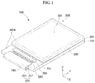
- FIG. 1 is a plan view of an organic light emitting diode (“OLED”) display device according to an embodiment of the present disclosure.
- FIG. 2 is a cross-sectional view of an OLED display device of FIG. 1 .
- FIG. 3 illustrates a side surface portion of an OLED display device according to an embodiment of the present disclosure.
- FIG. 4 illustrates a side surface portion of an OLED display device according to an embodiment of the present disclosure
- FIG. 5 illustrates a side surface portion of an OLED display device according to an embodiment of the present disclosure.
- FIG. 6 illustrates a side surface portion of an OLED display device according to an embodiment of the present disclosure.
- thicknesses of a plurality of layers and areas may be enlarged for clarity and ease of description thereof.
- a layer, area, or plate is referred to as being “on” another layer, area, or plate, it may be directly on the other layer, area, or plate, or intervening layers, areas, or plates may be present therebetween.
- a display device according to an exemplary embodiment will be described in detail with reference to FIGS. 1 through 6 .
- a display device will be described with respect to an organic light emitting diode (“OLED”) display device for ease of description.
- OLED organic light emitting diode
- FIG. 1 is a plan view of an organic light emitting diode (“OLED”) display device 100
- FIG. 2 is a cross-sectional view of the OLED display device 100 .
- the OLED display device 100 includes a display panel 200 , a connection unit 240 , a printed circuit board 270 , a driving chip 250 , a window 400 , and a black matrix 410 .
- the display panel 200 is for displaying images, and may be one of a liquid crystal display (“LCD”) panel, an electrophoretic display panel (“EDP”), an OLED display panel, a light emitting diode (“LED”) display panel, an inorganic electro luminescent (“EL”) display panel, a field emission display (“FED”) panel, a surface conduction electron-emitter display (“SED”) panel, a plasma display panel (“PDP”), or a cathode ray tube (“CRT”) panel.
- LCD liquid crystal display
- EDP electrophoretic display panel
- OLED light emitting diode
- EL inorganic electro luminescent
- FED field emission display
- SED surface conduction electron-emitter display
- PDP plasma display panel
- CRT cathode ray tube
- the display panel 200 includes a first substrate 101 , a second substrate 201 that opposes the first substrate 101 , a display unit 150 , a sealing member 300 , a touch unit 210 , and a polarizer 220 .
- the first substrate 101 includes a display area DA that displays images by emitting light, and a non-display area NDA located outside the display area DA. A plurality of pixels are formed in the display area DA of the first substrate 101 to display images.
- the display unit 150 is disposed in the display area DA.
- the non-display area NDA includes a pad area PA in which a plurality of pad electrodes 280 are formed and that receive external signals and transmit the signals to the OED to control light emission.
- At least one driving chip 250 is formed on the pad area PA.
- the first substrate 101 includes a transparent glass material that includes, for example, silicon oxide (SiO 2 ) as a main component.
- a transparent glass material that includes, for example, silicon oxide (SiO 2 ) as a main component.
- SiO 2 silicon oxide
- exemplary embodiments are not limited thereto, and the first substrate 101 may include a transparent plastic material.
- the driving chip 250 includes a scan driver and a data driver for driving the pixels.
- the first substrate 101 further includes pad electrodes disposed in the pad area PA.
- the driving chip 250 is mounted in the pad area PA of the first substrate 101 as a chip on glass (COG) and is electrically connected to the pad electrodes 280 .
- the driving chip 250 generates scan signals and data signals in response to driving power and signals received from the printed circuit board 270 .
- the scan signals and the data signals are transmitted to gate lines and data lines of the display area DA through the pad electrodes 280 .
- the driving chip 250 is not formed in the non-display area NDA and may be omitted.
- the driving chip 250 may be mounted on a flexible printed circuit board as a chip on film (“COF”). That is, a tape carrier package (“TCP”) scheme in which the driving chip 250 is mounted on the film in the form of a chip can be incorporated into the OLED display device 100 .
- COF chip on film
- TCP tape carrier package
- a pad that protects the driving chip 250 against external impacts is further disposed in the pad area PA.
- the driving chip 250 is an integrated circuit (“IC”) chip such as a driving IC.
- the display unit 150 is formed on the first substrate 101 , and is connected to the driving chip 250 .
- the display unit 150 includes an OLED, and a thin film transistor and wirings that drive the OLED. Those elements other than the OLED that serve the function of the display device are considered part of the display unit 150 .
- the second substrate 201 is disposed opposite from the first substrate 101 , and is attached to the first substrate 101 by the sealing member 300 .
- the second substrate 201 may include a glass substrate, or may include a transparent synthetic resin film, such as an acrylic film.
- the second substrate 201 includes a metal plate.
- the second substrate 201 includes one of a polyethylene (PET) film, a polypropylene (PP) film, a polyamide (PA) film, a polyacetal (POM) film, a poly methyl methacrylate (PMMA) film, a polybutylene terephthalate (PBT) film, a polycarbonate (PC) film, a cellulose film, or a moisture-resistant cellophane.
- the second substrate 201 has a planar area less than a planar area of the first substrate 101 . Accordingly, the pad area PA of the first substrate 101 is exposed by the second substrate 201 .
- the sealing member 300 includes a commonly used material, such as a sealing glass frit.
- the touch unit 210 is disposed on the second substrate 201 in an area that corresponds to the display area DA of the first substrate 101 .
- the touch unit 210 includes first and second electrodes that cross each other.
- the first and second electrodes each have a plurality of columns that together form a matrix and are directly patterned on the second substrate 201 as an on-cell type.
- the first and second electrodes correspond to a touch sensor pattern.
- the touch unit 210 may be disposed on the second substrate 201 as a separately manufactured touch panel.
- the touch unit 210 can detect a touch input by a touch means, such as a pen or a user's finger, and transmits a signal that corresponds to a touched location to a touch driving unit.
- the touch unit 210 is used as an input means for the OLED display device 100 and may be a resistive type or a capacitive type.
- the window 400 includes a transparent material, such as glass or a resin.
- the window 400 protects the display panel 200 from being broken by external impacts.
- the window 400 is disposed on the touch unit 210 and covers the display area DA and the pad area PA.
- the window 400 is attached to the second substrate 201 by an adhesive layer 230 .
- the window 400 is larger in size than the display panel 200 .
- exemplary embodiments are not limited thereto, and the window 400 may be substantially the same size as the display panel 200 .
- the black matrix 410 is disposed in an area of the window 400 that corresponds to the pad area PA.
- the black matrix 410 includes a printing material that substantially prevents a pattern below the window 400 from being visible.
- the printing material includes a black printing material, but the color of the printing material may vary depending on the design of a device to be realized.
- the black matrix 410 includes a light absorbing material such as chromium (Cr).
- the polarizer 220 is disposed between the window 400 and the touch unit 210 .
- the polarizer 220 substantially prevents reflection of external light.
- the adhesive layer 230 is disposed between the window 400 and the touch unit 210 , and improves the luminance, transmittance, reflectance, and visibility of the OLED display device 100 .
- the adhesive layer 230 substantially prevents formation of an air gap between the window 400 and the second substrate 201 , and substantially prevents penetration of foreign substances, such as dust.
- the adhesive layer 230 is a resin.
- the resin is a photo-curable resin.
- the printed circuit board 270 transmits driving signals to the display panel 200 .
- the printed circuit board 270 includes, inter alia, a timing controller that generates control signals that drive the display panel 200 and a power voltage generator that generates a power voltage.
- the printed circuit board 270 is disposed on one surface of the display panel 200 . More specifically, the printed circuit board 270 is disposed on a back surface of the display panel 200 .
- the display panel 200 displays images on an upper surface of the display panel 200 , and the back surface of the display panel 200 is unseen by a user. Accordingly, the printed circuit board 270 can be disposed on the back surface of the display panel 200 to maximize space efficiency and to hide a configuration that a user does not need to see.
- exemplary embodiments are not limited thereto, and the printed circuit board 270 may be disposed on a side surface of the display panel 200 , or the printed circuit board and the flexible printed circuit board may be formed into a unitary structure.
- the printed circuit board 270 since the printed circuit board 270 transmits driving signals to the display panel 200 , the printed circuit board 270 is electrically connected to the display panel 200 . Accordingly, the connection unit 240 electrically connects the display panel 200 and the printed circuit board 270 .
- connection unit 240 is connected to the pad area PA of the display panel 200 .
- the connection unit 240 provides an electrical connection between the display panel 200 and the printed circuit board 270 .
- the connection unit 240 is a flexible printed circuit board (“FPCB”).
- the connection unit 240 may be a tape carrier package or a chip on film that includes an integrated circuit (“IC”) chip.
- connection unit 240 includes an overlap portion 241 that contacts the pad area PA of the display panel 200 , and a curved surface portion 242 that is curved along the side surface of the display panel 200 .
- the connection unit 240 includes the overlap portion 241 that contacts the pad area PA of the first substrate 101 , and the curved surface portion 242 that is curved along the side surface of the first substrate 101 .
- connection unit 240 one end portion of the connection unit 240 is electrically connected to the display panel 200 , and another end portion of the connection unit 240 is electrically connected to the printed circuit board 270 . Accordingly, the display panel 200 and the printed circuit board 270 are electrically connected to each other by the connection unit 240 .
- connection unit 240 includes a base film and a wiring pattern on the base film, and further includes a cover film on the wiring pattern.
- the wiring pattern is disposed between the base film and the cover film.
- the wiring pattern transmits electrical signals and includes a metal such as copper (Cu).
- a metal such as copper (Cu).
- tin, silver, nickel, etc. may be plated on the copper surface.
- Wiring patterns may be formed through various methods, such as casting, laminating, electroplating, etc.
- connection unit 240 is electrically connected to the display panel 200
- another end portion of the connection unit 240 is electrically connected to the printed circuit board 270 .
- the one end portion and the other end portion of the connection unit 240 correspond to the overlap portion 241 .
- the curved surface portion 242 is formed along the side surface of the display panel 200 between the one end portion and the other end portion of the connection unit 240 .
- the curved surface portion 242 surrounds the side surface of the display panel 200 .
- the radius of curvature of the curved surface portion 242 becomes smaller, which increases stress, and a phenomenon in which the overlap portion 241 of the connection unit 240 detaches from the display panel 200 can occur.
- the OLED display device 100 includes a filler 260 disposed between the side surface of the display panel 200 and the connection unit 240 .
- the filler 260 is disposed between the curved surface portion 242 of the connection unit 240 and the side surface of the display panel 200 .
- the filler 260 is disposed between the side surface of the first substrate 101 and the curved surface portion 242 , as illustrated in FIG. 2 .
- the filler 260 includes a resin 261 and a heat dissipating material 262 dispersed in the resin 261 .
- the resin 261 is a sticky material that can be rapidly cured by ultraviolet light (UV).
- UV ultraviolet light
- As the resin 261 is disposed on the curved surface portion 242 of the connection unit 240 an air gap which was present between the display panel 200 and the connection unit 240 is removed. Accordingly, attachment of the connection unit 240 to the display panel 200 is improved by the resin 261 of the filler 260 , and the mechanical strength of the OLED display device 100 is improved.
- a heat dissipation material 262 dissipates heat generated in the driving chip 250 and the connection unit 240 .
- the heat dissipation material 262 includes at least one of gold, silver, copper, tungsten, carbon nanotube (CNT), graphite, or a mixture thereof.
- the heat dissipation material 262 includes small particles of a material such as copper or graphite, etc.
- the heat dissipation material 262 can include a metal having high thermal conductivity.
- connection unit 240 that are connected to the pad electrode 280 are bent and connected to the printed circuit board 270 therebelow, in which case the wiring can be damaged.
- FIG. 3 illustrates a side surface portion of an OLED display device according to an embodiment of the present disclosure.
- an OLED display device includes a flexible display substrate 610 , a touch layer 600 , a polarizer 590 , a first adhesive layer 620 , a second adhesive layer 640 , a connection pad 550 , a driving chip 561 mounted as a chip on film (“COF”), a printed circuit board 580 , and a filler layer 630 .
- COF chip on film
- the touch layer 600 is disposed on the flexible display substrate 610 , and the polarizer 590 is disposed on the touch layer 600 .
- the flexible substrate 610 includes a bent portion 510 where the substrate is bent, and the bent portion 510 includes an upper bent portion 530 and a lower bent portion 540 .
- a lower surface of the flexible substrate 610 is attached to the first adhesive layer 620 and the second adhesive layer 640 , and the filler layer 630 is disposed between the first adhesive layer 620 and the second adhesive layer 640 .
- a film 560 on which the driving chip 561 is mounted is attached to the second adhesive layer 640 , and an upper portion of the printed circuit board 580 and a lower portion of the film 560 are electrically connected to each other at one end portion of the printed circuit board 580 .
- the connection pad 550 includes an upper pad area 521 connected to the flexible display substrate 610 and a lower pad area 522 connected to the film 560 that connects the flexible display substrate 610 and the driving chip 561 .
- the upper pad area 521 includes a pad terminal, etc., and electrically connects the flexible display substrate 610 and the connection pad 550 .
- the lower pad area 522 includes a pad terminal, etc., and electrically connects the film 560 and the flexible display substrate 610 .
- the connection pad 550 is disposed on side surfaces of the flexible display substrate 610 and on opposite sides of the flexible display substrate 610 .
- the connection pad 550 includes silver.
- a display device further includes a connection pad disposed on one side surface of the display substrate 610 and that includes an upper pad area and a lower pad area, is connected to the touch layer 600 by the upper pad area 521 , the display substrate 610 by the lower pad area 522 , and overlaps the connection pad 550 .
- FIG. 4 illustrates a side surface portion of an OLED display device according to an embodiment of the present disclosure.
- an OLED display device 500 includes a flexible display substrate 610 , a touch layer 600 , a polarizer 590 , a first adhesive layer 620 , a second adhesive layer 640 , a connection pad 550 , a filler layer 630 , and a film 560 that includes a driving chip that drives the touch layer 600 .
- the touch layer 600 is disposed on the flexible display substrate 610
- the polarizer 590 is disposed on the touch layer 600 .
- the flexible substrate 610 includes a bent portion 510 where the substrate is bent, and the bent portion 510 includes an upper bent portion 530 and a lower bent portion 540 .
- a lower portion of the flexible substrate 610 is attached to the first adhesive layer 620 and the second adhesive layer 640
- the filler layer 630 is disposed between the first adhesive layer 620 and the second adhesive layer 640 .
- One end portion of the film 560 that includes a driving chip for driving the touch layer 600 is attached to the second adhesive layer 640 , and another end portion thereof is attached to the flexible display substrate 610 .
- the connection pad 550 includes an upper pad area 521 connected to the flexible display substrate 610 , and a lower pad area 522 connected to the film 560 .
- the upper pad area 521 includes a pad terminal, etc., and electrically connects the touch layer 600 and the connection pad 550 .
- the lower pad area 522 includes a pad terminal, etc., and is electrically connected to the display substrate 610 at a lower portion of the substrate 610 .
- the connection pad 550 is disposed on side surfaces of the flexible display substrate 610 and is disposed on opposite sides of the flexible display substrate 610 .
- connection pad 550 includes silver.
- the connection pad 550 connects the wiring of the touch layer 600 to the flexible display substrate 610 . Accordingly, damage to wirings connected to the touch layer 600 at the substrate bent portion 510 can be substantially prevented.
- connection pad 570 overlaps the connection pad 550 .
- the connection pad 570 is connected to the flexible display substrate 610 at an upper end 581 and a lower end 582 of the connection pad 570 .
- an insulating layer is disposed between the connection pad 550 and the connection pad 570 .
- connection pads 570 are disposed adjacent to one side surface of the flexible display substrate 610 and does not overlap the connection pad 550 .
- FIG. 5 illustrates a side surface portion of an OLED display device according to an embodiment of the present disclosure.
- an OLED display device 500 includes a flexible display substrate 610 , a touch layer 600 , a polarizer 590 , a first adhesive layer 620 , a second adhesive layer 640 , a connection pad 550 , a touch layer driving unit 650 mounted as a chip on pad (“COP”), and a filler layer 630 .
- COP chip on pad
- the touch layer 600 is disposed on the flexible display substrate 610
- the polarizer 590 is disposed on the touch layer 600 .
- the flexible display substrate 610 includes a substrate bent portion 510
- the substrate bent portion 510 includes an upper substrate bent portion 530 and a lower substrate bent portion 540 .
- a lower portion of the flexible substrate 610 is attached to the first adhesive layer 620 and the second adhesive layer 640
- the filler layer 630 is disposed between the first adhesive layer 620 and the second adhesive layer 640 .
- the touch layer driving unit 650 includes a driving chip 660 that drives the touch layer 600 and is attached to a lower portion of the flexible display substrate 610 .
- the connection pad 550 includes an upper pad area 521 connected to the touch layer 600 and a lower pad area 522 connected to a pad on which the driving chip 660 is mounted.
- the upper pad area 521 includes a pad terminal, etc., that electrically connects the touch layer 600 and the connection pad 550 .
- the lower pad area 522 includes a pad terminal, etc., and is electrically connected to the touch layer driving unit 650 .
- the touch layer driving unit 650 is attached to a lower portion of the display substrate 610 , and is vertically connected to the connection pad 550 .
- the touch layer driving unit 650 includes the driving chip 660 that drives the touch layer 600 , and includes a contact portion 670 that is vertically connected to the connection pad 550 .
- connection pad 550 is disposed on side surfaces of the flexible display substrate 610 , and the connection pad 550 is disposed on opposite side surfaces of the flexible display substrate 610 .
- connection pad 550 includes silver.
- connection pad 550 connects the wiring of the touch layer 600 to the flexible display substrate 610 on the side surface thereof. Accordingly, wiring connected to the touch layer 600 can be removed from the substrate bent portion 510 , and damage to the wiring connected to the touch layer 600 at the substrate bent portion 510 can be substantially prevented.
- another connection pad 570 is attached inside the connection pad 550 .
- the connection pad 570 is connected to the flexible display substrate 610 at an upper end 581 and a lower end 582 .
- an insulating layer is disposed between the connection pad 550 and the connection pad 570 .
- the connection pad 570 overlaps the connection pad 550 .
- a printed circuit board connected to the touch layer driving unit 650 is further included.
- FIG. 6 illustrates a side surface portion of an OLED display device according to an embodiment of the present disclosure.
- an OLED display device 500 includes a flexible display substrate 610 , a touch layer 600 , a polarizer 590 , a first adhesive layer 620 , a second adhesive layer 640 , a connection pad 550 , and a filler layer 630 .
- the touch layer 600 is disposed on the flexible display substrate 610
- the polarizer 590 is disposed on the touch layer 600 .
- the flexible substrate 610 includes a substrate bent portion 510
- the substrate bent portion 510 includes an upper substrate bent portion 530 and a lower substrate bent portion 540 .
- a lower portion of the flexible substrate 610 is attached to the first adhesive layer 620 and the second adhesive layer 640
- the filler layer 630 is disposed between the first adhesive layer 620 and the second adhesive layer 640 .
- the connection pad 550 includes an upper pad area 521 connected to the flexible display substrate 610 , and a lower pad area 522 connected to the flexible display substrate 610 .
- the upper pad area 521 and the lower pad area 522 include a pad terminal that electrically connects the touch layer 600 and the connection pad 550 .
- the upper pad area 521 includes a two-layer terminal which contacts the touch layer 600 and transmits signals of the touch layer 600 .
- the lower pad area 522 includes a pad terminal, etc., and is electrically connected to the flexible display substrate 610 .
- the connection pad 550 are disposed on side surfaces of the flexible display substrate 610 , and the connection pad 550 are disposed on opposite side surfaces of the flexible display substrate 610 .
- the connection pad 550 includes silver.
- connection pad 550 connects the wiring of the touch layer 600 to the flexible display substrate 610 on the side surface thereof. Accordingly, wiring connected to the touch layer 600 can be removed from the substrate bent portion 510 , and thus damage to the wirings connected to the touch layer 600 at the substrate bent portion 510 can be substantially prevented.
- another connection pad 570 is attached inside the connection pad 550 .
- the connection pad 570 is connected to the flexible display substrate 610 at an upper end 581 and a lower end 582 .
- an insulating layer is disposed between the connection pad 550 and the connection pad 570 .
- the connection pad 570 overlaps the connection pad 550 .
- a connection pad on a side surface of a display device to connect substrates.
Landscapes
- Engineering & Computer Science (AREA)
- General Engineering & Computer Science (AREA)
- Theoretical Computer Science (AREA)
- Physics & Mathematics (AREA)
- Human Computer Interaction (AREA)
- General Physics & Mathematics (AREA)
- Computer Networks & Wireless Communication (AREA)
- Optics & Photonics (AREA)
- Manufacturing & Machinery (AREA)
- Microelectronics & Electronic Packaging (AREA)
- Electroluminescent Light Sources (AREA)
- Devices For Indicating Variable Information By Combining Individual Elements (AREA)
Abstract
Description
Claims (20)
Applications Claiming Priority (2)
| Application Number | Priority Date | Filing Date | Title |
|---|---|---|---|
| KR10-2017-0183275 | 2017-12-29 | ||
| KR1020170183275A KR102457907B1 (en) | 2017-12-29 | 2017-12-29 | Display device |
Publications (2)
| Publication Number | Publication Date |
|---|---|
| US20190206898A1 US20190206898A1 (en) | 2019-07-04 |
| US11329068B2 true US11329068B2 (en) | 2022-05-10 |
Family
ID=67058483
Family Applications (1)
| Application Number | Title | Priority Date | Filing Date |
|---|---|---|---|
| US16/193,001 Active 2038-12-17 US11329068B2 (en) | 2017-12-29 | 2018-11-16 | Display device |
Country Status (2)
| Country | Link |
|---|---|
| US (1) | US11329068B2 (en) |
| KR (1) | KR102457907B1 (en) |
Cited By (1)
| Publication number | Priority date | Publication date | Assignee | Title |
|---|---|---|---|---|
| US11468832B2 (en) * | 2019-11-08 | 2022-10-11 | Beijing Boe Technology Development Co., Ltd. | Array substrate and method for manufacturing same, display panel, and display device |
Families Citing this family (11)
| Publication number | Priority date | Publication date | Assignee | Title |
|---|---|---|---|---|
| TWI682221B (en) * | 2018-05-22 | 2020-01-11 | 鴻海精密工業股份有限公司 | Electronic device and method for making electronic device |
| US10950670B2 (en) * | 2018-12-17 | 2021-03-16 | Wuhan China Star Optoelectronics Semiconductor Display Technology Co., Ltd. | Display panel |
| CN111489634A (en) * | 2019-01-25 | 2020-08-04 | 格科微电子(上海)有限公司 | Display panel of portable electronic device and design method thereof |
| CN209216555U (en) * | 2019-01-29 | 2019-08-06 | 合肥京东方显示技术有限公司 | A kind of flip chip and display device |
| KR20200136548A (en) * | 2019-05-27 | 2020-12-08 | 삼성디스플레이 주식회사 | Display device |
| CN110515501B (en) * | 2019-09-02 | 2021-09-14 | 京东方科技集团股份有限公司 | Display device and method for manufacturing the same |
| KR102787589B1 (en) | 2020-02-18 | 2025-03-28 | 삼성디스플레이 주식회사 | Display device |
| CN113823654B (en) * | 2020-06-19 | 2024-03-15 | 京东方科技集团股份有限公司 | A driving substrate, a light-emitting device and a manufacturing method thereof |
| KR102873685B1 (en) * | 2021-11-15 | 2025-10-17 | 엘지디스플레이 주식회사 | Display apparatus |
| KR20230097264A (en) | 2021-12-23 | 2023-07-03 | 삼성디스플레이 주식회사 | Electronic device |
| KR20230115381A (en) * | 2022-01-26 | 2023-08-03 | 삼성디스플레이 주식회사 | Display device and tile-type display device including same |
Citations (11)
| Publication number | Priority date | Publication date | Assignee | Title |
|---|---|---|---|---|
| KR20130078143A (en) | 2011-12-30 | 2013-07-10 | 엘지디스플레이 주식회사 | Organic light emitting display device |
| US20140042406A1 (en) | 2012-08-07 | 2014-02-13 | Apple Inc. | Flexible Displays |
| US20140085585A1 (en) | 2012-09-21 | 2014-03-27 | Samsung Display Co., Ltd. | Display panel having larger display area and method of manufacturing the same |
| KR20140136233A (en) | 2013-05-20 | 2014-11-28 | 엘지전자 주식회사 | Display Panel and Display Apparatus |
| KR20140136237A (en) | 2013-05-20 | 2014-11-28 | 엘지전자 주식회사 | Display Panel and Display Apparatus |
| KR20140136238A (en) | 2013-05-20 | 2014-11-28 | 엘지전자 주식회사 | Display Panel and Display Apparatus |
| US9123593B2 (en) | 2013-05-20 | 2015-09-01 | Lg Electronics Inc. | Display panel and display device |
| US20160093685A1 (en) * | 2014-09-30 | 2016-03-31 | Lg Display Co., Ltd. | Flexible display device with bend stress reduction member and manufacturing method for the same |
| KR20170034040A (en) | 2015-09-18 | 2017-03-28 | 엘지디스플레이 주식회사 | Display device |
| US20170207276A1 (en) * | 2016-01-15 | 2017-07-20 | Japan Display Inc. | Display device |
| US20180164913A1 (en) * | 2015-08-10 | 2018-06-14 | Dongwoo Fine-Chem Co., Ltd. | Electrode connection and electric device comprising the same |
-
2017
- 2017-12-29 KR KR1020170183275A patent/KR102457907B1/en active Active
-
2018
- 2018-11-16 US US16/193,001 patent/US11329068B2/en active Active
Patent Citations (14)
| Publication number | Priority date | Publication date | Assignee | Title |
|---|---|---|---|---|
| KR20130078143A (en) | 2011-12-30 | 2013-07-10 | 엘지디스플레이 주식회사 | Organic light emitting display device |
| US20140042406A1 (en) | 2012-08-07 | 2014-02-13 | Apple Inc. | Flexible Displays |
| US20140085585A1 (en) | 2012-09-21 | 2014-03-27 | Samsung Display Co., Ltd. | Display panel having larger display area and method of manufacturing the same |
| KR20140038823A (en) | 2012-09-21 | 2014-03-31 | 삼성디스플레이 주식회사 | Display panel and method of fabricating the same |
| KR20140136238A (en) | 2013-05-20 | 2014-11-28 | 엘지전자 주식회사 | Display Panel and Display Apparatus |
| KR20140136237A (en) | 2013-05-20 | 2014-11-28 | 엘지전자 주식회사 | Display Panel and Display Apparatus |
| KR20140136233A (en) | 2013-05-20 | 2014-11-28 | 엘지전자 주식회사 | Display Panel and Display Apparatus |
| US9123593B2 (en) | 2013-05-20 | 2015-09-01 | Lg Electronics Inc. | Display panel and display device |
| US9366929B2 (en) | 2013-05-20 | 2016-06-14 | Lg Electronics, Inc. | Display panel and display device |
| US9632381B2 (en) | 2013-05-20 | 2017-04-25 | Lg Electronics Inc. | Display panel and display device |
| US20160093685A1 (en) * | 2014-09-30 | 2016-03-31 | Lg Display Co., Ltd. | Flexible display device with bend stress reduction member and manufacturing method for the same |
| US20180164913A1 (en) * | 2015-08-10 | 2018-06-14 | Dongwoo Fine-Chem Co., Ltd. | Electrode connection and electric device comprising the same |
| KR20170034040A (en) | 2015-09-18 | 2017-03-28 | 엘지디스플레이 주식회사 | Display device |
| US20170207276A1 (en) * | 2016-01-15 | 2017-07-20 | Japan Display Inc. | Display device |
Cited By (2)
| Publication number | Priority date | Publication date | Assignee | Title |
|---|---|---|---|---|
| US11468832B2 (en) * | 2019-11-08 | 2022-10-11 | Beijing Boe Technology Development Co., Ltd. | Array substrate and method for manufacturing same, display panel, and display device |
| US11893930B2 (en) | 2019-11-08 | 2024-02-06 | Boe Technology Group Co., Ltd. | Array substrate, display panel, and display device |
Also Published As
| Publication number | Publication date |
|---|---|
| KR20190082338A (en) | 2019-07-10 |
| KR102457907B1 (en) | 2022-10-25 |
| US20190206898A1 (en) | 2019-07-04 |
Similar Documents
| Publication | Publication Date | Title |
|---|---|---|
| US11329068B2 (en) | Display device | |
| CN109597516B (en) | display screen | |
| US9661744B2 (en) | Touch panel having a sensing electrode and a printing electrode | |
| EP3026536A1 (en) | Touch window comprising mesh electrode | |
| US10347864B2 (en) | Display device | |
| US20120127095A1 (en) | Flat panel display with an integrated touch screen panel | |
| US20150234503A1 (en) | Touch sensing apparatus and method for manufacturing the same | |
| CN111354765A (en) | Flexible display device | |
| KR20080091609A (en) | Touch screen display | |
| CN104423715A (en) | Touch window and display including the same | |
| US20200026391A1 (en) | Touchscreen panel and display device including the same | |
| US12089381B2 (en) | Display device | |
| KR20190120849A (en) | Display device | |
| US10908733B2 (en) | Display device and method of manufacturing the same | |
| CN108647586A (en) | Display device | |
| KR102794200B1 (en) | Electronic apparatus | |
| US11553604B2 (en) | Display apparatus | |
| CN110571321B (en) | electronic device | |
| KR102029710B1 (en) | Touch panel | |
| US20210343824A1 (en) | Display device | |
| KR20160000242A (en) | Touch window | |
| KR102861443B1 (en) | Display device | |
| KR102262549B1 (en) | Touch panel | |
| KR20160070537A (en) | Touch window | |
| CN120103990A (en) | Display device |
Legal Events
| Date | Code | Title | Description |
|---|---|---|---|
| AS | Assignment |
Owner name: SAMSUNG DISPLAY CO., LTD., KOREA, REPUBLIC OF Free format text: ASSIGNMENT OF ASSIGNORS INTEREST;ASSIGNOR:BAEK, SEUNGHO;REEL/FRAME:047522/0815 Effective date: 20181030 |
|
| FEPP | Fee payment procedure |
Free format text: ENTITY STATUS SET TO UNDISCOUNTED (ORIGINAL EVENT CODE: BIG.); ENTITY STATUS OF PATENT OWNER: LARGE ENTITY |
|
| STPP | Information on status: patent application and granting procedure in general |
Free format text: NON FINAL ACTION MAILED |
|
| STPP | Information on status: patent application and granting procedure in general |
Free format text: RESPONSE AFTER FINAL ACTION FORWARDED TO EXAMINER |
|
| STPP | Information on status: patent application and granting procedure in general |
Free format text: NON FINAL ACTION MAILED |
|
| STPP | Information on status: patent application and granting procedure in general |
Free format text: RESPONSE TO NON-FINAL OFFICE ACTION ENTERED AND FORWARDED TO EXAMINER |
|
| STPP | Information on status: patent application and granting procedure in general |
Free format text: FINAL REJECTION MAILED |
|
| STPP | Information on status: patent application and granting procedure in general |
Free format text: RESPONSE AFTER FINAL ACTION FORWARDED TO EXAMINER |
|
| STPP | Information on status: patent application and granting procedure in general |
Free format text: ADVISORY ACTION MAILED |
|
| STPP | Information on status: patent application and granting procedure in general |
Free format text: DOCKETED NEW CASE - READY FOR EXAMINATION |
|
| STPP | Information on status: patent application and granting procedure in general |
Free format text: NON FINAL ACTION MAILED |
|
| STPP | Information on status: patent application and granting procedure in general |
Free format text: RESPONSE TO NON-FINAL OFFICE ACTION ENTERED AND FORWARDED TO EXAMINER |
|
| STPP | Information on status: patent application and granting procedure in general |
Free format text: NOTICE OF ALLOWANCE MAILED -- APPLICATION RECEIVED IN OFFICE OF PUBLICATIONS |
|
| STPP | Information on status: patent application and granting procedure in general |
Free format text: AWAITING TC RESP., ISSUE FEE NOT PAID |
|
| STPP | Information on status: patent application and granting procedure in general |
Free format text: AWAITING TC RESP, ISSUE FEE PAYMENT VERIFIED |
|
| STPP | Information on status: patent application and granting procedure in general |
Free format text: PUBLICATIONS -- ISSUE FEE PAYMENT VERIFIED |
|
| STCF | Information on status: patent grant |
Free format text: PATENTED CASE |
|
| MAFP | Maintenance fee payment |
Free format text: PAYMENT OF MAINTENANCE FEE, 4TH YEAR, LARGE ENTITY (ORIGINAL EVENT CODE: M1551); ENTITY STATUS OF PATENT OWNER: LARGE ENTITY Year of fee payment: 4 |