US11327770B2 - Data storage devices, access device and data processing methods - Google Patents
Data storage devices, access device and data processing methods Download PDFInfo
- Publication number
- US11327770B2 US11327770B2 US16/721,887 US201916721887A US11327770B2 US 11327770 B2 US11327770 B2 US 11327770B2 US 201916721887 A US201916721887 A US 201916721887A US 11327770 B2 US11327770 B2 US 11327770B2
- Authority
- US
- United States
- Prior art keywords
- system data
- memory device
- memory
- predetermined
- data
- Prior art date
- Legal status (The legal status is an assumption and is not a legal conclusion. Google has not performed a legal analysis and makes no representation as to the accuracy of the status listed.)
- Active, expires
Links
Images


Classifications
-
- G—PHYSICS
- G06—COMPUTING OR CALCULATING; COUNTING
- G06F—ELECTRIC DIGITAL DATA PROCESSING
- G06F3/00—Input arrangements for transferring data to be processed into a form capable of being handled by the computer; Output arrangements for transferring data from processing unit to output unit, e.g. interface arrangements
- G06F3/06—Digital input from, or digital output to, record carriers, e.g. RAID, emulated record carriers or networked record carriers
- G06F3/0601—Interfaces specially adapted for storage systems
- G06F3/0602—Interfaces specially adapted for storage systems specifically adapted to achieve a particular effect
- G06F3/061—Improving I/O performance
-
- G—PHYSICS
- G11—INFORMATION STORAGE
- G11C—STATIC STORES
- G11C29/00—Checking stores for correct operation ; Subsequent repair; Testing stores during standby or offline operation
- G11C29/04—Detection or location of defective memory elements, e.g. cell constructio details, timing of test signals
- G11C29/08—Functional testing, e.g. testing during refresh, power-on self testing [POST] or distributed testing
- G11C29/12—Built-in arrangements for testing, e.g. built-in self testing [BIST] or interconnection details
- G11C29/38—Response verification devices
-
- G—PHYSICS
- G06—COMPUTING OR CALCULATING; COUNTING
- G06F—ELECTRIC DIGITAL DATA PROCESSING
- G06F11/00—Error detection; Error correction; Monitoring
- G06F11/07—Responding to the occurrence of a fault, e.g. fault tolerance
- G06F11/08—Error detection or correction by redundancy in data representation, e.g. by using checking codes
- G06F11/10—Adding special bits or symbols to the coded information, e.g. parity check, casting out 9's or 11's
- G06F11/1008—Adding special bits or symbols to the coded information, e.g. parity check, casting out 9's or 11's in individual solid state devices
- G06F11/1044—Adding special bits or symbols to the coded information, e.g. parity check, casting out 9's or 11's in individual solid state devices with specific ECC/EDC distribution
-
- G—PHYSICS
- G06—COMPUTING OR CALCULATING; COUNTING
- G06F—ELECTRIC DIGITAL DATA PROCESSING
- G06F11/00—Error detection; Error correction; Monitoring
- G06F11/07—Responding to the occurrence of a fault, e.g. fault tolerance
- G06F11/14—Error detection or correction of the data by redundancy in operations
- G06F11/1402—Saving, restoring, recovering or retrying
- G06F11/1415—Saving, restoring, recovering or retrying at system level
- G06F11/1417—Boot up procedures
-
- G—PHYSICS
- G06—COMPUTING OR CALCULATING; COUNTING
- G06F—ELECTRIC DIGITAL DATA PROCESSING
- G06F3/00—Input arrangements for transferring data to be processed into a form capable of being handled by the computer; Output arrangements for transferring data from processing unit to output unit, e.g. interface arrangements
- G06F3/06—Digital input from, or digital output to, record carriers, e.g. RAID, emulated record carriers or networked record carriers
- G06F3/0601—Interfaces specially adapted for storage systems
- G06F3/0628—Interfaces specially adapted for storage systems making use of a particular technique
- G06F3/0646—Horizontal data movement in storage systems, i.e. moving data in between storage devices or systems
- G06F3/065—Replication mechanisms
-
- G—PHYSICS
- G06—COMPUTING OR CALCULATING; COUNTING
- G06F—ELECTRIC DIGITAL DATA PROCESSING
- G06F3/00—Input arrangements for transferring data to be processed into a form capable of being handled by the computer; Output arrangements for transferring data from processing unit to output unit, e.g. interface arrangements
- G06F3/06—Digital input from, or digital output to, record carriers, e.g. RAID, emulated record carriers or networked record carriers
- G06F3/0601—Interfaces specially adapted for storage systems
- G06F3/0628—Interfaces specially adapted for storage systems making use of a particular technique
- G06F3/0655—Vertical data movement, i.e. input-output transfer; data movement between one or more hosts and one or more storage devices
- G06F3/0658—Controller construction arrangements
-
- G—PHYSICS
- G06—COMPUTING OR CALCULATING; COUNTING
- G06F—ELECTRIC DIGITAL DATA PROCESSING
- G06F3/00—Input arrangements for transferring data to be processed into a form capable of being handled by the computer; Output arrangements for transferring data from processing unit to output unit, e.g. interface arrangements
- G06F3/06—Digital input from, or digital output to, record carriers, e.g. RAID, emulated record carriers or networked record carriers
- G06F3/0601—Interfaces specially adapted for storage systems
- G06F3/0668—Interfaces specially adapted for storage systems adopting a particular infrastructure
- G06F3/0671—In-line storage system
- G06F3/0673—Single storage device
- G06F3/0679—Non-volatile semiconductor memory device, e.g. flash memory, one time programmable memory [OTP]
-
- G—PHYSICS
- G06—COMPUTING OR CALCULATING; COUNTING
- G06F—ELECTRIC DIGITAL DATA PROCESSING
- G06F3/00—Input arrangements for transferring data to be processed into a form capable of being handled by the computer; Output arrangements for transferring data from processing unit to output unit, e.g. interface arrangements
- G06F3/06—Digital input from, or digital output to, record carriers, e.g. RAID, emulated record carriers or networked record carriers
- G06F3/0601—Interfaces specially adapted for storage systems
- G06F3/0668—Interfaces specially adapted for storage systems adopting a particular infrastructure
- G06F3/0671—In-line storage system
- G06F3/0683—Plurality of storage devices
- G06F3/0688—Non-volatile semiconductor memory arrays
-
- G—PHYSICS
- G06—COMPUTING OR CALCULATING; COUNTING
- G06F—ELECTRIC DIGITAL DATA PROCESSING
- G06F9/00—Arrangements for program control, e.g. control units
- G06F9/06—Arrangements for program control, e.g. control units using stored programs, i.e. using an internal store of processing equipment to receive or retain programs
- G06F9/44—Arrangements for executing specific programs
- G06F9/4401—Bootstrapping
- G06F9/4403—Processor initialisation
-
- G—PHYSICS
- G11—INFORMATION STORAGE
- G11C—STATIC STORES
- G11C29/00—Checking stores for correct operation ; Subsequent repair; Testing stores during standby or offline operation
- G11C29/04—Detection or location of defective memory elements, e.g. cell constructio details, timing of test signals
- G11C29/08—Functional testing, e.g. testing during refresh, power-on self testing [POST] or distributed testing
- G11C29/12—Built-in arrangements for testing, e.g. built-in self testing [BIST] or interconnection details
- G11C29/44—Indication or identification of errors, e.g. for repair
Definitions
- the invention relates to a data processing method for a memory device, which is capable of solving the problem with the conventional design wherein system data stored in the memory device cannot be successfully accessed after the memory device has undergone a high-temperature bonding procedure.
- a data storage device, an access device and a data processing method are provided.
- An exemplary embodiment of a data storage device comprises a memory device and a memory controller.
- the memory device comprises a plurality of memory blocks.
- the memory controller is coupled to the memory device and configured to access the memory device.
- the memory controller is configured to perform an initialization procedure to initialize the memory device. In the initialization procedure, the memory controller is configured to read a boot code index stored in the memory device and to try to read predetermined system data from a predetermined address indicated by the boot code index.
- the memory controller is further configured to perform a duplicate obtaining procedure to obtain system data that is complete and correct from one or more duplicates of the predetermined system data.
- the boot code index is further utilized to indicate a copy rule.
- the memory controller is further configured to determine addresses of the memory device for storing the duplicates of the predetermined system data according to the copy rule and/or the predetermined address, and read the duplicates of the predetermined system data to obtain the system data that is complete and correct.
- An exemplary embodiment of an access device comprises a memory controller coupled to a memory device and configured to access the memory device.
- the memory controller is configured to perform a test procedure on the memory device to obtain a test result, and configured to write a boot code index, which indicates a predetermined address for storing predetermined system data of the memory device and a copy rule adopted for generating one or more duplicates of the predetermined system data, in the memory device.
- the memory controller is further configured to establish system data of the memory device according to the test result, write the system data into the predetermined address as the predetermined system data, and store the system data in one or more memory blocks of the memory device as duplicates of the predetermined system data according to the copy rule.
- An exemplary embodiment of a data processing method for processing data of a memory device comprises the following steps performed by a first memory controller: performing a test procedure on the memory device to obtain a test result; writing a boot code index in the memory device, wherein the boot code index indicates a predetermined address for storing predetermined system data of the memory device and a copy rule adopted for generating one or more duplicates of the predetermined system data; establishing system data of the memory device according to the test result; writing the system data into the predetermined address as the predetermined system data; and storing the system data in one or more memory blocks of the memory device as duplicates of the predetermined system data according to the copy rule.
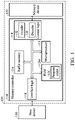
- FIG. 1 shows an exemplary block diagram of a data storage device according to an embodiment of the invention
- FIG. 2 is a schematic diagram showing the three stages for manufacturing a memory product according to an embodiment of the invention.
- FIG. 3 is a flow chart of a data processing method according to an embodiment of the invention.
- FIG. 4 is a flow chart of a data processing method according to an embodiment of the invention.
- FIG. 1 shows an exemplary block diagram of a data storage device according to an embodiment of the invention.
- the data storage device 100 may comprise a memory device 120 , such as a flash memory module, and a memory controller 110 .
- the memory controller 110 is configured to access the memory device 120 .
- the memory controller 110 may comprise a microprocessor 112 , a Read Only Memory (ROM) 112 M, a control logic 114 , a buffer memory 116 and an interface logic 118 .
- the ROM 112 M is configured to store program codes 112 C.
- the microprocessor 112 is configured to execute the program codes 112 C, thereby controlling access to the memory device 120 .
- the control logic 114 may comprise an encoder 132 and a decoder 134 .
- the encoder 132 is configured to encode the data to be written into the memory device 120 so as to generate corresponding correcting/checking code (also called error correction code (ECC)).
- ECC error correction code
- the decoder 134 is
- the memory device 120 may comprise a plurality of flash memory chips, and each flash memory chip may comprise a plurality of memory blocks.
- the access unit of an erase operation performed by the controller (e.g., the memory controller 110 , through the execution of the program codes 112 C by the microprocessor 112 ) on the memory device 120 may be one memory block.
- a memory block may record (comprise) a predetermined number of pages, that is, the physical pages, and the access unit of a write operation performed by the controller (e.g., the memory controller 110 , through the execution of the program codes 112 C by the microprocessor 112 ) on the memory device 120 may be one page.
- the memory controller 110 may perform various control operations by using its own internal components through the execution of the program codes 112 C by the microprocessor 112 .
- the memory controller 110 may use the control logic 114 to control the access operations (especially the access operation for at least a memory block or at least a page) of the memory device 120 , use the buffer memory 116 to perform necessary data buffer operations, and use the interface logic 118 to communicate with a host device 130 .
- the buffer memory 116 may be implemented by a Random Access Memory (RAM).
- the buffer memory 116 may be an SRAM, but the invention should not be limited thereto.
- the data storage device 100 may be a portable storage device (for example, the memory card in compliance with the SD/MMC, CF, MS and/or XD standard), and the host device 130 may be an electronic device, such as a mobile phone, a notebook computer, a desktop computer . . . etc., capable of connecting to the data storage device.
- the data storage device 100 may be a solid state hard disk or an embedded storage device in compliance with the Universal Flash Storage (UFS) or the Embedded Multi Media Card (EMMC) standards, and may be equipped in an electronic device such as a mobile phone, a notebook computer, or a desktop computer.
- the host device 130 may be a processor of the electronic device.
- the data storage device 100 may be a specialized access device comprising a memory controller and one or more sockets (not shown in the figure).
- the memory device 120 can be installed in the data storage device 110 in a removable manner
- the host device 130 may be an electronic device, such as a mobile phone, a notebook computer, a desktop computer . . . etc., capable of connecting to the data storage device.
- the specialized access device may be utilized to perform product test on one or more memory devices at the same time. Via the product test, information regarding the number of good and bad memory blocks of each memory device can be obtained and the quality of the memory device can be determined. The memory devices can be classified and configured according to the corresponding quality.
- the host device 130 may issue commands, such as the read command or the write command, to the data storage device 100 , so as to access the data stored in the memory device 120 , or the host device 130 may issue commands to further control or manage the data storage device 100 .
- the memory blocks comprised in the memory device 120 may be configured as the Single-Level Cell (SLC) memory blocks, the Multiple-Level Cell (MLC) memory blocks and/or the Triple-Level Cell (TLC) memory blocks.
- the memory cell of the SLC memory block is configured to store one bit data
- the memory cell of the MLC memory block is configured to store two bits data
- the memory cell of the TLC memory block is configured to store three bits data.
- the memory device 120 when making a memory device (e.g. the memory device 120 ) into a specific memory product, the memory device 120 may undergo three stages, comprising a test and classification stage, a bonding stage and an initialization stage.
- FIG. 2 is a schematic diagram showing the three stages for manufacturing a memory product according to an embodiment of the invention.
- the memory device 120 may be coupled to different memory controller in the test and classification stage and the initialization stage.
- the memory controller 120 may be coupled to a first memory controller.
- the first memory controller may be the memory controller comprised in the afore-mentioned specialized access device, and at this time, the first memory controller and the memory device 120 coupled to the first memory controller may be as a whole regarded as a data storage device, such as the afore-mentioned data storage device 100 .
- the memory device 120 may be removed from the specialized access device.
- Another memory device may then be coupled to the first memory controller when needed, so as to perform the test and classification on the next memory device via the first memory controller. Testing and classification can be repeatedly performed on different memory devices.
- the first memory controller may perform the read/write test multiple times on the memory device 120 coupled thereto, so as to determine which memory blocks are damaged, which memory blocks are good and available, calculate the actual usable capability of the memory device 120 as the size of the memory device 120 , determine the quality of the memory device 120 according to the damage rate of the memory blocks and classify the memory device 120 according to the quality of the memory device 120 (for example, determining whether the memory device 120 will be manufactured as a USB 2.0 product, a USB 3.0 product, an SSD product, or others), and set the corresponding memory configuration for the memory device 120 according to the quality thereof (for example, which kind of operation should be adopted (such as the one-plane operation, two-plane operation, four-plane operation, etc.), whether the memory device 120 should be operated in a reliable mode or an unreliable mode, which memory blocks should be configured as the memory blocks for storing system data, which memory blocks should be configured as the memory blocks for storing system data, etc.).
- the quality of the memory device 120 for example, determining whether the memory
- the afore-mentioned configuration and information regarding the settings of the memory device are the essential information required for accessing the memory device 120 subsequently. Therefore, in the test and classification stage, the first memory controller may obtain the information regarding the size of the memory device 120 and essential information required for accessing the memory device 120 , record the information as the system data of the memory device 120 , and write the system data into the memory device 120 .
- the memory device 120 can be removed from the access device and then the memory device 120 may be coupled to a corresponding second memory device based on the classification result. For example, when the memory device 120 is determined to be manufactured as a USB 3.0 product in the test and classification stage, the memory device 120 may then be coupled to a USB 3.0 memory controller. In the bonding stage, the memory device 120 and the second memory controller are bonded to the printed circuit board (PCB). For example, being bonded to the PCB by using surface mounting technology (SMT). The second memory controller and the memory device 120 coupled thereto may be as a whole regarded as another data storage device, for example, another data storage device 100 . Next, an initialization stage of the memory device 120 can be entered.
- PCB printed circuit board
- SMT surface mounting technology
- an initialization procedure is performed.
- the second memory controller has to read the afore-mentioned system data, so as to obtain the information regarding the size of the memory device 120 and essential information required for accessing the memory device 120 , and the second memory controller can perform some other necessary initialization operations on the memory device 120 according to the obtained information. Note that the necessary initialization operations may be different for different types of memory products.
- the second memory controller has to convert the data format of the obtained system data. After the data format conversion, the content of the system data can be recognized.
- the first memory controller and the second memory controller may have substantially the same design, or have similar design, and the difference is only in the content of the program codes 112 C, the interface logic to communicate with the memory device, the corresponding In-System Programming (ISP) codes, etc. Therefore, the structure of the first memory controller and the second memory controller (and the corresponding access device or data storage device) may refer to the block diagram shown in FIG. 1 . However, it is to be understood that those who are skilled in this technology can still make various alterations and modifications on the hardware design of the memory controller shown in FIG. 1 . Therefore, the structure and components comprised in the first memory controller and the second memory controller in practice should not be limited to what is shown in FIG. 1 .
- the system data stored in the memory device 120 may be damaged or lost, which may further cause the problem that the second memory controller is unable to obtain the system data.
- a data processing method and the corresponding data storage device and access device implementing the data processing method are provided. Via the special data processing performed by the first memory controller in the test and classification stage, it can ensure that the second memory controller is able to obtain system data that is complete and correct in the initialization stage.
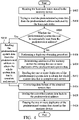
- FIG. 3 is a flow chart of a data processing method according to an embodiment of the invention.
- the memory device is first coupled to the first memory controller and the test and classification stage is entered.
- the first memory controller is configured to perform a test procedure on the memory device to obtain a test result (Step S 302 ).
- the first memory controller is configured to write a boot code index in the memory device (Step S 304 ).
- the boot code index may be limited only to be stored in a specific memory area of the memory device.
- the first memory controller may determine to store the system data in which position (address) as the predetermined system data and determine to adopt which copy rule for copying the system data as one or more duplicates of the predetermined system data.
- the content of the boot code index indicates a predetermined address for storing the predetermined system data and the copy rule adopted for generating duplicates of the predetermined system data.
- the first memory controller is configured to establish the system data of the memory device according to the test result (Step S 306 ), and write the system data into the predetermined address as the predetermined system data (Step S 308 ).
- the system data comprises information regarding the size of the memory device and essential information required for accessing the memory device.
- the first memory controller is further configured to write (or, store) the system data in one or more memory blocks of the memory device as duplicates of the predetermined system data according to the copy rule (Step S 310 ).
- FIG. 4 is a flow chart of a data processing method according to an embodiment of the invention.
- the second portion of the proposed data processing method is shown. That is, the flow chart of the proposed data processing method in the initialization stage subsequent to the test and classification stage.
- the first memory controller is de-coupled from the memory device, and the second memory controller is coupled to the memory device.
- the second memory controller is the corresponding controller of the final memory product that will comprise the memory device.
- the second memory controller is configured to read the boot code index stored in the memory device (Step S 402 ).
- the boot code index may be limited to only be stored in a specific memory area.
- the second memory controller may try to find out where the boot code index is in this specific memory area, so as to obtain the information regarding the predetermined address for storing predetermined system data of the memory device and the copy rule adopted for generating one or more duplicates of the predetermined system data.
- the second memory controller is configured to try to read the predetermined system data from the predetermined address indicated by the boot code index to obtain system data that is complete and correct (Step S 404 ).
- the second memory controller may further determine whether the predetermined system data can be successfully read from the predetermined address (Step S 406 ). For example, the second memory controller may determine whether the predetermined system data can be successfully read from the predetermined address based on whether the content of the header of the data stored in the predetermined address can be read successfully. When the second memory controller cannot successfully read the content of the header, it is determined that the second memory controller is also unable to successfully read the content of the predetermined system data from the predetermined address.
- the second memory controller may read the predetermined system data from the predetermined address to obtain system data that is complete and correct (Step S 414 ).
- the second memory controller may perform a duplicate obtaining procedure (Step S 408 ) to obtain system data that is complete and correct from one or more duplicates of the predetermined system data.
- the second memory controller may determine addresses of the memory device for storing the duplicates of the predetermined system data (Step S 410 ) according to the copy rule and/or the predetermined address indicated by the boot code index.
- the second memory controller may read the duplicates of the predetermined system data to obtain system data that is complete and correct (Step S 412 ).
- the second memory controller may convert the data format of the obtained system data (Step S 416 ), store the converted system data back in the predetermined address (Step S 418 ) and erase the duplicates of the predetermined system data stored in the memory device (Step S 420 ). That is, in the embodiment of the invention, only the system data stored in the predetermined address is preserved, and the duplicates or copies of the system data will be erased.
- the format conversion step (step S 416 ) is an optional choice. When the data format required by the final product that is to be made up of the memory device 120 will be the same as the one used in the test and classification stage, the step can be skipped.
- the first memory controller is not limited to only store the duplicates of the predetermined system data in the memory blocks that are configured for storing system data.
- the first memory controller may also store the duplicates of the predetermined system data in the memory blocks that are configured for storing user data. Since the duplicates of the predetermined system data will finally be deleted (for example, being erased in step S 420 ), in the embodiments of the invention, the first memory controller may store the duplicates of the predetermined system data in the memory blocks that are configured for storing user data, and this will not cause the user problems with insufficient available memory space.
- the first memory controller may select a proper copy rule from a group of predefined copy rules for generating duplicates of the predetermined system data.
- the way to copy the system data may be mainly divided into two types, including a first type: to store or copy all of the system data in one memory block and a second type: to store or copy only one page of the system data in one memory block.
- the first memory controller may select M memory blocks and store the N pages of complete system data in each selected memory block, wherein N and M are positive integers.
- one memory block may be utilized to store the content of one predetermined page of the system data, and a plurality of pages comprised in this memory block will all be written with the same content of the predetermined page.
- the system data comprises N pages of data, wherein N is a positive integer
- the first memory controller may select M memory blocks, and different memory blocks may be utilized to store different pages of the system data, wherein M is a positive integer greater than or equal to N.
- some or all of the pages comprised in a first memory block may be utilized to store the content of the first page of the system data
- a plurality of pages or all pages comprised in a second memory block may be utilized to store the content of the second page of the system data, and so on.
- the first memory controller may also select the memory blocks utilized to store the duplicates according to a variety of different rules. For example, the first memory controller may select the memory blocks determined as having good quality to store the duplicates. In addition, for example, since the memory blocks determined as having good quality are usually configured as the memory blocks for storing the system data, the first memory controller may select the memory blocks utilized configured for storing the system data to store the duplicates of the system data.
- the first memory controller may set a cardinal number n, where n is a positive integer, and the first memory controller may select the memory blocks having a corresponding memory block number (or, index) as a multiple of n as the memory blocks for storing the duplicates of the system data.
- the duplicates of the system data may be stored in the memory device based on a fixed data density.
- the duplicates of the system data may also be in the memory device according to different data densities.
- the first memory controller may select more memory blocks in the memory area having good quality, and select fewer memory blocks in the memory area having poor quality to store the duplicates of the system data.
- the memory area having good quality may be utilized to store the duplicates of the system data with higher data density
- the memory area having poor quality may be utilized to store the duplicates of the system data with lower data density.
- the quality of the memory area may be determined in the aforementioned test stage or may be pre-determined according to the previous experimental results.
- the first memory controller may select a proper copy rule from a group of predefined copy rules for generating duplicates of the predetermined system data.
- the predefined copy rules may comprise each combination of a way to copy the system data discussed above (for example, the first type, the second type, and a hybrid of the first type and the second type) and a way to select the memory blocks for storing the duplicates of the system data.
- each combination of the way to copy the system data and the way to select the memory block may be assigned with a corresponding number (that is, the number of the copy rule). After determining to use which way to copy the system data and use which way to select the memory block, the number of the corresponding copy rule may be recorded in one or more bytes of the boot code index.
- the boot code index may comprise the information regarding the predetermined address of the predetermined system data and the number of the copy rule.
- the predetermined address may be the physical address of the memory device.
- ALE address latch enable
- the number of the copy rule may be a serial number.
- the second memory controller may determine addresses of the memory device for storing the duplicates of the predetermined system data according to the copy rule and/or the predetermined address indicated by the boot code index, so as to read the duplicates of the predetermined system data to obtain system data that is complete and correct. For example, when the way to select the memory blocks of the adopted copy rule is related to the predetermined address, the second memory controller may determine the locations of the memory blocks utilized to store the duplicates of the system dada according to the copy rule and the predetermined address indicated by the boot code index. When the way to select the memory blocks of the adopted copy rule and the predetermined address are unrelated, the second memory controller may directly determine the locations of the memory blocks utilized to store the duplicates of the system dada according to the copy rule indicated by the boot code index.
- the second memory controller is configured to read the duplicates of the predetermined system data according to the copy rule indicated by the boot code index to obtain system data that is complete and correct.
- the second memory controller may use a variety of different ways to obtain system data that is complete and correct.
- the second memory device may collect the correct pages of the system data page by page, and store the content of the obtained correct pages in the buffer memory 116 . The operations can be repeated until all the correct pages of the system data have been collected.
- the source for providing the correct page of the system data may also be the predetermined system data. That is, one or more correct pages of the system data may be collected from the predetermined system data.
- the second memory controller may try to find the whole system data that is complete and correct from one memory block. If there is any page that is incorrect, the second memory controller may discard this memory block and try another memory block storing the duplicates. In another example, the second memory controller may first try to find the whole system data that is complete and correct from one memory block. If the second memory controller is unable to collect the whole system data that is complete and correct within one memory block, the second memory controller may change the way to collect the system data by collecting the correct pages of the system data page by page.
- the first memory controller may select a proper copy rule for generating one or more duplicates of the predetermined system data and select one or more proper memory blocks for storing the duplicates according to the copy rule, so as to ensure that the second memory controller is able to obtain the whole system data that is complete and correct in the initialization stage.
- the second memory controller may try to read the original system data, that is, the aforementioned predetermined system data, according to the predetermined address indicated by the boot code index.
- a duplicate obtaining procedure When the second memory controller is unable to successfully read the predetermined system data, a duplicate obtaining procedure will be triggered.
- the second memory controller obtains the way to copy the system data and the addresses of the memory blocks storing the duplicates of the system data according to the copy rule (or further according to the predetermined address) indicated by the boot code index.
- the duplicates stored in one or more memory blocks By reading the duplicates stored in one or more memory blocks, the whole system data that is complete and correct can be obtained.
- the (converted) system data is stored back in the predetermined address and the memory blocks storing the duplicates will be erased, so as to release the memory space.
Landscapes
- Engineering & Computer Science (AREA)
- Theoretical Computer Science (AREA)
- Physics & Mathematics (AREA)
- General Engineering & Computer Science (AREA)
- General Physics & Mathematics (AREA)
- Software Systems (AREA)
- Human Computer Interaction (AREA)
- Computer Security & Cryptography (AREA)
- Quality & Reliability (AREA)
- Techniques For Improving Reliability Of Storages (AREA)
Abstract
Description
Claims (9)
Applications Claiming Priority (2)
| Application Number | Priority Date | Filing Date | Title |
|---|---|---|---|
| TW108100034 | 2019-01-02 | ||
| TW108100034A TWI698748B (en) | 2019-01-02 | 2019-01-02 | Data storage device, access device and data processing method |
Publications (2)
| Publication Number | Publication Date |
|---|---|
| US20200210202A1 US20200210202A1 (en) | 2020-07-02 |
| US11327770B2 true US11327770B2 (en) | 2022-05-10 |
Family
ID=71123000
Family Applications (1)
| Application Number | Title | Priority Date | Filing Date |
|---|---|---|---|
| US16/721,887 Active 2040-08-12 US11327770B2 (en) | 2019-01-02 | 2019-12-19 | Data storage devices, access device and data processing methods |
Country Status (3)
| Country | Link |
|---|---|
| US (1) | US11327770B2 (en) |
| CN (1) | CN111399758B (en) |
| TW (1) | TWI698748B (en) |
Citations (8)
| Publication number | Priority date | Publication date | Assignee | Title |
|---|---|---|---|---|
| US20070266202A1 (en) * | 2005-06-13 | 2007-11-15 | Naoki Mukaida | Memory controller, flash memory system, and control method of flash memory |
| US20090222689A1 (en) * | 2006-08-24 | 2009-09-03 | Vipul Patel | Memory device internal parameter reliability |
| US20110238629A1 (en) * | 2010-03-23 | 2011-09-29 | Apple Inc. | Uncorrectable error handling schemes for non-volatile memories |
| US20120246384A1 (en) * | 2011-03-21 | 2012-09-27 | Winbond Electronics Corp. | Flash memory and flash memory accessing method |
| US20140250295A1 (en) * | 2011-10-26 | 2014-09-04 | John J Briden | Load boot data |
| US20180173536A1 (en) * | 2016-12-15 | 2018-06-21 | Western Digital Technologies, Inc. | Non-volatile storage device with multiple boot partitions |
| US10073651B2 (en) * | 2016-09-19 | 2018-09-11 | SK Hynix Inc. | Memory system with power-off detection and recovery mechanism |
| US10102081B2 (en) * | 2014-06-26 | 2018-10-16 | Rambus Inc. | Memory controller system with non-volatile backup storage |
Family Cites Families (7)
| Publication number | Priority date | Publication date | Assignee | Title |
|---|---|---|---|---|
| US7383362B2 (en) * | 2003-12-02 | 2008-06-03 | Super Talent Electronics, Inc. | Single-chip multi-media card/secure digital (MMC/SD) controller reading power-on boot code from integrated flash memory for user storage |
| TWI319139B (en) * | 2006-11-29 | 2010-01-01 | Inventec Corp | Method for repairing the data of double flash roms and synchronizing data between the two flash roms |
| CN101187879B (en) * | 2007-12-27 | 2011-01-12 | 威盛电子股份有限公司 | Electronic system and its data processing method |
| TWI383399B (en) * | 2009-03-03 | 2013-01-21 | Wistron Corp | Embedded electronic device and method for storing data |
| CN103578566B (en) * | 2012-07-23 | 2016-08-24 | 群联电子股份有限公司 | Memory storage device and repair method thereof |
| TWI659307B (en) * | 2017-01-06 | 2019-05-11 | 慧榮科技股份有限公司 | Data storage device and flash memory control method |
| TWI639917B (en) * | 2017-04-25 | 2018-11-01 | 慧榮科技股份有限公司 | Data storage device and mapping table reconstruction method |
-
2019
- 2019-01-02 TW TW108100034A patent/TWI698748B/en active
- 2019-10-24 CN CN201911016804.XA patent/CN111399758B/en active Active
- 2019-12-19 US US16/721,887 patent/US11327770B2/en active Active
Patent Citations (8)
| Publication number | Priority date | Publication date | Assignee | Title |
|---|---|---|---|---|
| US20070266202A1 (en) * | 2005-06-13 | 2007-11-15 | Naoki Mukaida | Memory controller, flash memory system, and control method of flash memory |
| US20090222689A1 (en) * | 2006-08-24 | 2009-09-03 | Vipul Patel | Memory device internal parameter reliability |
| US20110238629A1 (en) * | 2010-03-23 | 2011-09-29 | Apple Inc. | Uncorrectable error handling schemes for non-volatile memories |
| US20120246384A1 (en) * | 2011-03-21 | 2012-09-27 | Winbond Electronics Corp. | Flash memory and flash memory accessing method |
| US20140250295A1 (en) * | 2011-10-26 | 2014-09-04 | John J Briden | Load boot data |
| US10102081B2 (en) * | 2014-06-26 | 2018-10-16 | Rambus Inc. | Memory controller system with non-volatile backup storage |
| US10073651B2 (en) * | 2016-09-19 | 2018-09-11 | SK Hynix Inc. | Memory system with power-off detection and recovery mechanism |
| US20180173536A1 (en) * | 2016-12-15 | 2018-06-21 | Western Digital Technologies, Inc. | Non-volatile storage device with multiple boot partitions |
Also Published As
| Publication number | Publication date |
|---|---|
| TW202026888A (en) | 2020-07-16 |
| US20200210202A1 (en) | 2020-07-02 |
| CN111399758A (en) | 2020-07-10 |
| CN111399758B (en) | 2023-08-01 |
| TWI698748B (en) | 2020-07-11 |
Similar Documents
| Publication | Publication Date | Title |
|---|---|---|
| CN110335635B (en) | Method for managing a memory device and memory device and controller | |
| US11010065B2 (en) | Read retry method for solid state storage device | |
| US8516184B2 (en) | Data updating using mark count threshold in non-volatile memory | |
| US9176865B2 (en) | Data writing method, memory controller, and memory storage device | |
| US11216381B2 (en) | Data storage devices and data processing methods | |
| US9177656B2 (en) | Data writing method, memory storage device and memory controlling circuit unit | |
| US10606744B2 (en) | Method for accessing flash memory module and associated flash memory controller and electronic device | |
| US11204864B2 (en) | Data storage devices and data processing methods for improving the accessing performance of the data storage devices | |
| US11176033B2 (en) | Data storage devices and data processing methods | |
| US8301981B2 (en) | Data access method for flash memory and storage system and controller thereof | |
| US9552287B2 (en) | Data management method, memory controller and embedded memory storage apparatus using the same | |
| US10871909B2 (en) | Block management method, memory control circuit unit and apparatus using mapping tables and block recognition machine learning with block parameters as training data | |
| US12211547B2 (en) | Dummy data-based read reference voltage search of NAND memory | |
| US8812772B2 (en) | Data merging method for non-volatile memory and controller and storage apparatus using the same | |
| US10579289B2 (en) | Memory management method for configuring super physical units of rewritable non-volatile memory modules, memory control circuit unit and memory storage device | |
| CN113741798A (en) | Data storage device and operation method thereof | |
| US20140089566A1 (en) | Data storing method, and memory controller and memory storage apparatus using the same | |
| US11662940B2 (en) | Data storage device and data processing method for restoring MLC/TLC memory to avoid degradation of access performance of a memory device caused by word line short | |
| US11307786B2 (en) | Data storage devices and data processing methods | |
| US8276033B2 (en) | Data writing method for a flash memory, and flash memory controller and flash memory storage apparatus using the same | |
| US11327770B2 (en) | Data storage devices, access device and data processing methods | |
| US20090182932A1 (en) | Method for managing flash memory blocks and controller using the same | |
| CN115048051B (en) | Data reading method, memory controller and memory storage device | |
| CN114627941B (en) | Memory management method, memory storage device and memory control circuit unit | |
| US10942858B2 (en) | Data storage devices and data processing methods |
Legal Events
| Date | Code | Title | Description |
|---|---|---|---|
| AS | Assignment |
Owner name: SILICON MOTION, INC., TAIWAN Free format text: ASSIGNMENT OF ASSIGNORS INTEREST;ASSIGNOR:WU, PO-WEI;REEL/FRAME:051339/0464 Effective date: 20191216 |
|
| FEPP | Fee payment procedure |
Free format text: ENTITY STATUS SET TO UNDISCOUNTED (ORIGINAL EVENT CODE: BIG.); ENTITY STATUS OF PATENT OWNER: LARGE ENTITY |
|
| STPP | Information on status: patent application and granting procedure in general |
Free format text: DOCKETED NEW CASE - READY FOR EXAMINATION |
|
| STPP | Information on status: patent application and granting procedure in general |
Free format text: NON FINAL ACTION MAILED |
|
| STPP | Information on status: patent application and granting procedure in general |
Free format text: RESPONSE TO NON-FINAL OFFICE ACTION ENTERED AND FORWARDED TO EXAMINER |
|
| STPP | Information on status: patent application and granting procedure in general |
Free format text: NOTICE OF ALLOWANCE MAILED -- APPLICATION RECEIVED IN OFFICE OF PUBLICATIONS |
|
| STPP | Information on status: patent application and granting procedure in general |
Free format text: AWAITING TC RESP, ISSUE FEE PAYMENT VERIFIED |
|
| STPP | Information on status: patent application and granting procedure in general |
Free format text: PUBLICATIONS -- ISSUE FEE PAYMENT VERIFIED |
|
| STCF | Information on status: patent grant |
Free format text: PATENTED CASE |
|
| MAFP | Maintenance fee payment |
Free format text: PAYMENT OF MAINTENANCE FEE, 4TH YEAR, LARGE ENTITY (ORIGINAL EVENT CODE: M1551); ENTITY STATUS OF PATENT OWNER: LARGE ENTITY Year of fee payment: 4 |