US11315766B2 - Plasma processing apparatus and method for measuring thickness of ring member - Google Patents
Plasma processing apparatus and method for measuring thickness of ring member Download PDFInfo
- Publication number
- US11315766B2 US11315766B2 US16/590,953 US201916590953A US11315766B2 US 11315766 B2 US11315766 B2 US 11315766B2 US 201916590953 A US201916590953 A US 201916590953A US 11315766 B2 US11315766 B2 US 11315766B2
- Authority
- US
- United States
- Prior art keywords
- ring member
- jig
- mounting surface
- thickness
- processing apparatus
- Prior art date
- Legal status (The legal status is an assumption and is not a legal conclusion. Google has not performed a legal analysis and makes no representation as to the accuracy of the status listed.)
- Active, expires
Links
Images


Classifications
-
- H—ELECTRICITY
- H01—ELECTRIC ELEMENTS
- H01J—ELECTRIC DISCHARGE TUBES OR DISCHARGE LAMPS
- H01J37/00—Discharge tubes with provision for introducing objects or material to be exposed to the discharge, e.g. for the purpose of examination or processing thereof
- H01J37/32—Gas-filled discharge tubes
- H01J37/32431—Constructional details of the reactor
- H01J37/32623—Mechanical discharge control means
- H01J37/32642—Focus rings
-
- H—ELECTRICITY
- H01—ELECTRIC ELEMENTS
- H01J—ELECTRIC DISCHARGE TUBES OR DISCHARGE LAMPS
- H01J37/00—Discharge tubes with provision for introducing objects or material to be exposed to the discharge, e.g. for the purpose of examination or processing thereof
- H01J37/02—Details
- H01J37/244—Detectors; Associated components or circuits therefor
-
- G—PHYSICS
- G01—MEASURING; TESTING
- G01B—MEASURING LENGTH, THICKNESS OR SIMILAR LINEAR DIMENSIONS; MEASURING ANGLES; MEASURING AREAS; MEASURING IRREGULARITIES OF SURFACES OR CONTOURS
- G01B21/00—Measuring arrangements or details thereof, where the measuring technique is not covered by the other groups of this subclass, unspecified or not relevant
- G01B21/02—Measuring arrangements or details thereof, where the measuring technique is not covered by the other groups of this subclass, unspecified or not relevant for measuring length, width, or thickness
- G01B21/08—Measuring arrangements or details thereof, where the measuring technique is not covered by the other groups of this subclass, unspecified or not relevant for measuring length, width, or thickness for measuring thickness
-
- H—ELECTRICITY
- H01—ELECTRIC ELEMENTS
- H01J—ELECTRIC DISCHARGE TUBES OR DISCHARGE LAMPS
- H01J37/00—Discharge tubes with provision for introducing objects or material to be exposed to the discharge, e.g. for the purpose of examination or processing thereof
- H01J37/32—Gas-filled discharge tubes
- H01J37/32431—Constructional details of the reactor
- H01J37/32715—Workpiece holder
-
- H01L21/67069—
-
- H01L21/67253—
-
- H01L21/6833—
-
- H—ELECTRICITY
- H05—ELECTRIC TECHNIQUES NOT OTHERWISE PROVIDED FOR
- H05H—PLASMA TECHNIQUE; PRODUCTION OF ACCELERATED ELECTRICALLY-CHARGED PARTICLES OR OF NEUTRONS; PRODUCTION OR ACCELERATION OF NEUTRAL MOLECULAR OR ATOMIC BEAMS
- H05H1/00—Generating plasma; Handling plasma
- H05H1/24—Generating plasma
- H05H1/46—Generating plasma using applied electromagnetic fields, e.g. high frequency or microwave energy
-
- H—ELECTRICITY
- H10—SEMICONDUCTOR DEVICES; ELECTRIC SOLID-STATE DEVICES NOT OTHERWISE PROVIDED FOR
- H10P—GENERIC PROCESSES OR APPARATUS FOR THE MANUFACTURE OR TREATMENT OF DEVICES COVERED BY CLASS H10
- H10P50/00—Etching of wafers, substrates or parts of devices
- H10P50/20—Dry etching; Plasma etching; Reactive-ion etching
- H10P50/24—Dry etching; Plasma etching; Reactive-ion etching of semiconductor materials
- H10P50/242—Dry etching; Plasma etching; Reactive-ion etching of semiconductor materials of Group IV materials
-
- H—ELECTRICITY
- H10—SEMICONDUCTOR DEVICES; ELECTRIC SOLID-STATE DEVICES NOT OTHERWISE PROVIDED FOR
- H10P—GENERIC PROCESSES OR APPARATUS FOR THE MANUFACTURE OR TREATMENT OF DEVICES COVERED BY CLASS H10
- H10P72/00—Handling or holding of wafers, substrates or devices during manufacture or treatment thereof
- H10P72/04—Apparatus for manufacture or treatment
- H10P72/0402—Apparatus for fluid treatment
- H10P72/0418—Apparatus for fluid treatment for etching
- H10P72/0421—Apparatus for fluid treatment for etching for drying etching
-
- H—ELECTRICITY
- H10—SEMICONDUCTOR DEVICES; ELECTRIC SOLID-STATE DEVICES NOT OTHERWISE PROVIDED FOR
- H10P—GENERIC PROCESSES OR APPARATUS FOR THE MANUFACTURE OR TREATMENT OF DEVICES COVERED BY CLASS H10
- H10P72/00—Handling or holding of wafers, substrates or devices during manufacture or treatment thereof
- H10P72/04—Apparatus for manufacture or treatment
- H10P72/0431—Apparatus for thermal treatment
- H10P72/0434—Apparatus for thermal treatment mainly by convection
-
- H—ELECTRICITY
- H10—SEMICONDUCTOR DEVICES; ELECTRIC SOLID-STATE DEVICES NOT OTHERWISE PROVIDED FOR
- H10P—GENERIC PROCESSES OR APPARATUS FOR THE MANUFACTURE OR TREATMENT OF DEVICES COVERED BY CLASS H10
- H10P72/00—Handling or holding of wafers, substrates or devices during manufacture or treatment thereof
- H10P72/06—Apparatus for monitoring, sorting, marking, testing or measuring
- H10P72/0604—Process monitoring, e.g. flow or thickness monitoring
-
- H—ELECTRICITY
- H10—SEMICONDUCTOR DEVICES; ELECTRIC SOLID-STATE DEVICES NOT OTHERWISE PROVIDED FOR
- H10P—GENERIC PROCESSES OR APPARATUS FOR THE MANUFACTURE OR TREATMENT OF DEVICES COVERED BY CLASS H10
- H10P72/00—Handling or holding of wafers, substrates or devices during manufacture or treatment thereof
- H10P72/06—Apparatus for monitoring, sorting, marking, testing or measuring
- H10P72/0606—Position monitoring, e.g. misposition detection or presence detection
-
- H—ELECTRICITY
- H10—SEMICONDUCTOR DEVICES; ELECTRIC SOLID-STATE DEVICES NOT OTHERWISE PROVIDED FOR
- H10P—GENERIC PROCESSES OR APPARATUS FOR THE MANUFACTURE OR TREATMENT OF DEVICES COVERED BY CLASS H10
- H10P72/00—Handling or holding of wafers, substrates or devices during manufacture or treatment thereof
- H10P72/70—Handling or holding of wafers, substrates or devices during manufacture or treatment thereof for supporting or gripping
- H10P72/72—Handling or holding of wafers, substrates or devices during manufacture or treatment thereof for supporting or gripping using electrostatic chucks
- H10P72/722—Details of electrostatic chucks
-
- H—ELECTRICITY
- H10—SEMICONDUCTOR DEVICES; ELECTRIC SOLID-STATE DEVICES NOT OTHERWISE PROVIDED FOR
- H10P—GENERIC PROCESSES OR APPARATUS FOR THE MANUFACTURE OR TREATMENT OF DEVICES COVERED BY CLASS H10
- H10P72/00—Handling or holding of wafers, substrates or devices during manufacture or treatment thereof
- H10P72/70—Handling or holding of wafers, substrates or devices during manufacture or treatment thereof for supporting or gripping
- H10P72/76—Handling or holding of wafers, substrates or devices during manufacture or treatment thereof for supporting or gripping using mechanical means, e.g. clamps or pinches
- H10P72/7604—Handling or holding of wafers, substrates or devices during manufacture or treatment thereof for supporting or gripping using mechanical means, e.g. clamps or pinches the wafers being placed on a susceptor, stage or support
- H10P72/7606—Handling or holding of wafers, substrates or devices during manufacture or treatment thereof for supporting or gripping using mechanical means, e.g. clamps or pinches the wafers being placed on a susceptor, stage or support characterised by edge clamping, e.g. clamping ring
-
- H—ELECTRICITY
- H10—SEMICONDUCTOR DEVICES; ELECTRIC SOLID-STATE DEVICES NOT OTHERWISE PROVIDED FOR
- H10P—GENERIC PROCESSES OR APPARATUS FOR THE MANUFACTURE OR TREATMENT OF DEVICES COVERED BY CLASS H10
- H10P72/00—Handling or holding of wafers, substrates or devices during manufacture or treatment thereof
- H10P72/70—Handling or holding of wafers, substrates or devices during manufacture or treatment thereof for supporting or gripping
- H10P72/76—Handling or holding of wafers, substrates or devices during manufacture or treatment thereof for supporting or gripping using mechanical means, e.g. clamps or pinches
- H10P72/7604—Handling or holding of wafers, substrates or devices during manufacture or treatment thereof for supporting or gripping using mechanical means, e.g. clamps or pinches the wafers being placed on a susceptor, stage or support
- H10P72/7611—Handling or holding of wafers, substrates or devices during manufacture or treatment thereof for supporting or gripping using mechanical means, e.g. clamps or pinches the wafers being placed on a susceptor, stage or support characterised by edge profile or support profile
-
- H—ELECTRICITY
- H10—SEMICONDUCTOR DEVICES; ELECTRIC SOLID-STATE DEVICES NOT OTHERWISE PROVIDED FOR
- H10P—GENERIC PROCESSES OR APPARATUS FOR THE MANUFACTURE OR TREATMENT OF DEVICES COVERED BY CLASS H10
- H10P72/00—Handling or holding of wafers, substrates or devices during manufacture or treatment thereof
- H10P72/70—Handling or holding of wafers, substrates or devices during manufacture or treatment thereof for supporting or gripping
- H10P72/76—Handling or holding of wafers, substrates or devices during manufacture or treatment thereof for supporting or gripping using mechanical means, e.g. clamps or pinches
- H10P72/7604—Handling or holding of wafers, substrates or devices during manufacture or treatment thereof for supporting or gripping using mechanical means, e.g. clamps or pinches the wafers being placed on a susceptor, stage or support
- H10P72/7612—Handling or holding of wafers, substrates or devices during manufacture or treatment thereof for supporting or gripping using mechanical means, e.g. clamps or pinches the wafers being placed on a susceptor, stage or support characterised by lifting arrangements, e.g. lift pins
-
- H—ELECTRICITY
- H01—ELECTRIC ELEMENTS
- H01J—ELECTRIC DISCHARGE TUBES OR DISCHARGE LAMPS
- H01J2237/00—Discharge tubes exposing object to beam, e.g. for analysis treatment, etching, imaging
- H01J2237/245—Detection characterised by the variable being measured
- H01J2237/24571—Measurements of non-electric or non-magnetic variables
-
- H—ELECTRICITY
- H01—ELECTRIC ELEMENTS
- H01J—ELECTRIC DISCHARGE TUBES OR DISCHARGE LAMPS
- H01J2237/00—Discharge tubes exposing object to beam, e.g. for analysis treatment, etching, imaging
- H01J2237/32—Processing objects by plasma generation
- H01J2237/33—Processing objects by plasma generation characterised by the type of processing
- H01J2237/334—Etching
- H01J2237/3343—Problems associated with etching
Definitions
- the present disclosure relates to a plasma processing apparatus, and a method for measuring a thickness of a ring member.
- a plasma processing apparatus for performing plasma processing such as etching or the like on a target object such as a semiconductor wafer (hereinafter, also referred to as “wafer”) or the like using plasma.
- a target object such as a semiconductor wafer (hereinafter, also referred to as “wafer”) or the like using plasma.
- parts in the chamber are consumed by the plasma processing.
- a ring member such as a focus ring that is disposed to surround an outer peripheral portion of a wafer to make the plasma uniform is quickly consumed because it is close to the plasma.
- the degree of consumption of the focus ring greatly affects processing results on the wafer.
- etching characteristics near the outer peripheral portion of the wafer deteriorate, thereby affecting the uniformity or the like.
- the present disclosure provides a technique capable of accurately measuring a thickness of a ring member with a simple configuration.
- a plasma processing apparatus comprising: a mounting table having a first mounting surface on which a target object or a jig is mounted and a second mounting surface on which a ring member is mounted, the jig being used for measuring a thickness of the ring member disposed around the target object and having a facing portion facing an upper surface of the ring member; one or more elevating mechanisms configured to lift or lower the ring member with respect to the second mounting surface; an acquisition unit configured to acquire gap information indicating a gap dimension between the second mounting surface and the facing portion of the jig mounted on the first mounting surface; a measurement unit configured to measure a lifted distance of the ring member from the second mounting surface when the upper surface of the ring member is in contact with the facing portion of the jig mounted on the first mounting surface by lifting the ring member by using the elevating mechanisms; and a thickness calculation unit configured to calculate the thickness of the ring member based on the gap dimension and the measured lifted distance of the ring member
- FIG. 1 is a schematic cross-sectional view showing a configuration of a plasma processing apparatus according to a first embodiment
- FIG. 2 is a schematic cross-sectional view showing a main configuration of a mounting table according to the first embodiment
- FIG. 3 is a block diagram showing a schematic configuration of a control unit for controlling the plasma processing apparatus according to the first embodiment
- FIG. 4 is a flowchart showing exemplary flow of a focus ring thickness measurement process
- FIGS. 5A and 5B explain the exemplary flow of the focus ring thickness measurement process
- FIGS. 6A and 6B explain another exemplary flow of the focus ring thickness measurement process
- FIGS. 7A and 7B explain still another exemplary flow of the focus ring thickness measurement process
- FIG. 8 is a block diagram showing a schematic configuration of a control unit for controlling a plasma processing apparatus according to a second embodiment.
- FIGS. 9A and 9B explain exemplary flow of a process of measuring a gap dimension using a jig.
- a plasma processing apparatus for performing plasma processing such as etching or the like on a target object such as a semiconductor wafer (hereinafter, also referred to as “wafer”) or the like using plasma.
- a target object such as a semiconductor wafer (hereinafter, also referred to as “wafer”) or the like using plasma.
- parts in the chamber are consumed by the plasma processing.
- a ring member such as a focus ring that is disposed to surround an outer peripheral portion of a wafer to make the plasma uniform is quickly consumed because it is close to the plasma.
- the degree of consumption of the focus ring greatly affects processing results on the wafer.
- etching characteristics near the outer peripheral portion of the wafer deteriorate, thereby affecting the uniformity or the like.
- a consumption amount of a focus ring is specified by measuring a thickness of a consumed focus ring with respect to a thickness of a new focus ring. Therefore, it is expected to highly accurately measure the thickness of the focus ring with a simple configuration.
- FIG. 1 is a schematic cross-sectional view showing a configuration of a plasma processing apparatus 10 according to a first embodiment.
- the plasma processing apparatus 10 includes an airtight processing chamber 1 that is electrically grounded.
- the processing chamber 1 has a cylindrical shape and is made of, e.g., aluminum or the like.
- the processing chamber 1 defines a processing space where plasma is generated.
- a mounting table 2 for horizontally supporting a semiconductor wafer (hereinafter, simply referred to as “wafer”) W that is a work-piece is disposed in the processing chamber 1 .
- the mounting table 2 supports not only the wafer W but also a jig 51 (see FIG. 2 ) used for measuring a thickness of the focus ring 5 disposed to surround the wafer W. The structure of the jig 51 will be described later.
- the mounting table 2 includes a base 2 a and an electrostatic chuck (ESC) 6 .
- ESC electrostatic chuck
- the base 2 a is made of a conductive metal, e.g., aluminum or the like, and serves as a lower electrode.
- the base 2 a is supported by a support 4 .
- the support 4 is supported by a support member 3 made of, e.g., quartz or the like.
- An annular focus ring 5 made of, e.g., single crystalline silicon, is disposed on an outer peripheral portion of the mounting table 2 .
- An upper surface of an outer peripheral portion of the base 2 a serves as a mounting surface 2 e on which the focus ring 5 is mounted.
- a cylindrical inner wall member 3 a made of, e.g., quartz or the like, is disposed in the processing chamber 1 to surround the peripheral portions of the mounting table 2 and the support 4 .
- a first RF power supply 10 a is connected to the base 2 a via a first matching unit (MU) 11 a
- a second RF power supply 10 b is connected to the base 2 a via a second matching unit (MU) 11 b
- the first RF power supply 10 a is configured to supply a high frequency power for plasma generation, which has a given frequency, to the base 2 a of the mounting table 2
- the second RF power supply 10 b is configured to supply a high frequency power for ion attraction (for bias), which has a frequency lower than that of the first RF power supply 10 a , to the base 2 a of the mounting table 2 .
- a shower head 16 serving as an upper electrode is disposed above the mounting table 2 to be opposite to the mounting table 2 in parallel therewith.
- the shower head 16 and the mounting table 2 function as a pair of electrodes (the upper electrode and the lower electrode).
- the electrostatic chuck 6 is formed in a disk shape with a flat upper surface serving as a mounting surface 6 c on which the jig 51 or the wafer W is mounted.
- the electrostatic chuck 6 is disposed at a central portion of the substrate 2 a when viewed from the top.
- the electrostatic chuck 6 has a structure in which an electrode 6 a is embedded in an insulator 6 b .
- a DC power supply 12 is connected to the electrode 6 a . When a DC voltage is applied from the DC power supply 12 to the electrode 6 a , the jig 51 or the wafer W is attracted and held by a Coulomb force.
- a coolant flow path 2 d is formed inside the mounting table 2 .
- a coolant inlet line 2 b and a coolant outlet line 2 c are connected to the coolant flow path 2 d .
- the mounting table 2 can be controlled to a given temperature by circulating a proper coolant, e.g., cooling water or the like, through the coolant flow path 2 d .
- a gas supply line 30 for supplying a cold heat transfer gas (backside gas) such as helium gas or the like to the backside of the wafer W is disposed to penetrate through the mounting table 2 and the like.
- the gas supply line 30 is connected to a gas supply source (not shown). With this configuration, the wafer W attracted and held by the electrostatic chuck 6 on the upper surface of the mounting table 2 can be controlled to a given temperature.
- a plurality of, e.g., three (only one is shown in FIG. 1 ) pin through-holes 200 is disposed at a portion corresponding to the mounting surface 6 c of the mounting table 2 .
- Lifter pins 61 are respectively disposed inside the pin through-holes 200 .
- the lifter pins 61 are connected to an elevating mechanism (EM) 62 .
- the elevating mechanism 62 lifts or lowers the lifter pins 61 so that the lifter pins 61 protrude beyond or retract below the mounting surface 6 c of the mounting table 2 .
- the tip ends of the lifter pins 61 protrude beyond the mounting surface 6 c of the mounting table 2 , and the wafer W is held above the mounting surface 6 c of the mounting table 2 .
- the tip ends of the lifter pins 61 are accommodated in the pin through-holes 200 , and the wafer W is mounted on the mounting surface 6 c of the mounting table 2 .
- the elevating mechanism 62 lifts or lowers the wafer W with respect to the mounting surface 6 c of the mounting table 2 using the lifter pins 61 .
- a plurality of, e.g., three (only one is shown in FIG. 1 ) pin through-holes 300 is disposed at a portion corresponding to the mounting surface 2 e of the mounting table 2 .
- Lifter pins 63 are respectively disposed inside the pin through-holes 300 .
- the lifter pins 63 are connected to an elevating mechanism (EM) 64 .
- the elevating mechanism 64 lifts or lowers the lifter pins 63 so that the lifter pins 63 protrude beyond or retract below the mounting surface 2 e of the mounting table 2 .
- the tip ends of the lifter pins 63 protrude beyond the mounting surface 2 e of the mounting table 2 , and the wafer W is held above the mounting surface 2 e of the mounting table 2 .
- the tip ends of the lifter pins 63 are accommodated in the pin through-holes 300 , and the wafer W is mounted on the mounting surface 2 e of the mounting table 2 .
- the elevating mechanism 64 lifts or lowers the wafer W with respect to the mounting surface 2 e of the mounting table 2 using the lifter pins 63 .
- the shower head 16 is disposed at a ceiling wall portion of the processing chamber 1 .
- the shower head 16 includes a main body 16 a and an upper ceiling plate 16 b serving as an electrode plate.
- the shower head 16 is supported at an upper portion of the processing chamber 1 through an insulating member 95 .
- the main body 16 a is made of a conductive material, e.g., aluminum having an anodically oxidized surface.
- the main body 16 a has a structure to detachably attach the upper ceiling plate 16 b at a bottom portion of the main body 16 a.
- a gas diffusion space 16 c is formed in the main body 16 a .
- a plurality of gas holes 16 d is formed in a bottom portion of the gas diffusion space 16 c to be positioned under the gas diffusion space 16 c .
- Gas inlet holes 16 e are formed through the upper ceiling plate 16 b in a thickness direction thereof. The gas inlet holes 16 e communicate with the gas holes 16 d , respectively. With this configuration, a processing gas supplied to the gas diffusion space 16 c is distributed in a shower-like manner into the processing chamber 1 through the gas holes 16 d and the gas inlet holes 16 e.
- a gas inlet port 16 g for introducing the processing gas into the gas diffusion space 16 c is formed in the main body 16 a .
- One end of a gas supply line 15 a is connected to the gas inlet port 16 g and the other end of the gas supply line 15 a is connected to a processing gas supply source (gas supply unit) (PGS) 15 for supplying a processing gas.
- a mass flor controller (MFC) 15 b and an opening/closing valve V 2 are disposed in the gas supply line 15 a in that order from an upstream side.
- the processing gas for plasma etching is supplied from the processing gas supply source 15 to the gas diffusion space 16 c through the gas supply line 15 a .
- the processing gas is distributed in a shower-like manner into the processing chamber 1 from the gas diffusion chamber 16 c through the gas holes 16 d and the gas inlet holes 16 e.
- a variable DC power supply 72 is electrically connected to the shower head 16 serving as the upper electrode through a low pass filter (LPF) 71 .
- the power supply of the variable DC power supply 72 can be on-off controlled by an on/off switch 73 .
- a current and a voltage of the variable DC power supply 72 and on/off operation of the on/off switch 73 are controlled by a control unit 100 to be described later.
- the on/off switch 73 is turned on by the control unit 100 and a given DC voltage is applied to the shower head 16 serving as the upper electrode, if necessary.
- a cylindrical grounding conductor 1 a extends upward from a sidewall of the processing chamber 1 to be located at a position higher than the shower head 16 .
- the cylindrical ground conductor 1 a has a ceiling wall at the top thereof.
- a gas exhaust port 81 is formed at a bottom of the processing chamber 1 .
- a first gas exhaust unit (GEU) 83 is connected to the gas exhaust port 81 through a gas exhaust line 82 .
- the first gas exhaust unit 83 has a vacuum pump. By operating the vacuum pump, a pressure in the processing chamber 1 can be decreased to a given vacuum level.
- a loading/unloading port 84 for the wafer W is disposed at the sidewall of the processing chamber 1 .
- a gate valve 85 for opening or closing the loading/unloading port 84 is disposed at the loading/unloading port 84 .
- a deposition shield member 86 is disposed along an inner surface of the sidewall of the processing chamber 1 .
- the deposition shield member 86 prevents etching by-product (deposits) from being attached to the processing chamber 1 .
- a conductive member (GND block) 89 is disposed at a portion of the deposition shield member 86 at substantially the same height as the height of the wafer W.
- the conductive member 89 is connected to the ground such that a potential for the ground can be controlled. Due to the presence of the conductive member 89 , abnormal discharge can be prevented.
- a deposition shield member 87 extending along the inner wall member 3 a is disposed at a lower end portion of the deposition shield member 86 .
- the deposition shield members 86 and 87 are detachably provided.
- the operation of the plasma processing apparatus 10 configured as described above is integrally controlled by the control unit 100 .
- the control unit 100 is, e.g., a computer, and controls the respective components of the plasma processing apparatus 10 .
- FIG. 2 is a schematic cross-sectional view showing the main configuration of the mounting table 2 according to the first embodiment.
- the mounting table 2 includes the base 2 a and the electrostatic chuck 6 .
- the electrostatic chuck 6 has a disk shape and is disposed at the central portion of the base 2 a to be coaxial with the base 2 a .
- the electrostatic chuck 6 has a configuration in which the electrode 6 a is embedded in the insulator 6 b .
- the upper surface of the electrostatic chuck 6 serves as the mounting surface 6 c on which the jig 51 or the wafer W is mounted.
- FIG. 2 shows a state where the jig 51 is mounted on the mounting surface 6 c .
- the upper surface of the outer peripheral portion of the base 2 a serves as the mounting surface 2 e on which the focus ring 5 is mounted.
- the mounting surface 6 c is an example of a first mounting surface
- the mounting surface 2 e is an example of a second mounting surface.
- the focus ring 5 is an annular member.
- the focus ring 5 is disposed to surround an outer peripheral portion of the base 2 a to be coaxial with the base 2 a .
- the focus ring 5 includes a body portion 5 a and a protruding portion 5 b projecting inward in a radial direction from an inner side surface of the body portion 5 a .
- the upper surface of the protruding portion 5 b is lower than the upper surface of the body portion 5 a .
- the upper surface of the focus ring 5 has different heights depending on positions in the radial direction. For example, the height of the upper surface of the body portion 5 a is higher than the height of the mounting surface 6 c .
- the height of the upper surface of the protrusion 5 b is lower than the height of the mounting surface 6 c .
- the focus ring 5 is an example of a ring member.
- the jig 51 is used for measuring a thickness of the focus ring 5 .
- the jig 51 has a facing portion 51 a facing the upper surface of the focus ring 5 .
- the facing portion 51 a of the jig 51 is positioned above the body portion 5 a and the protruding portion 5 b of the focus ring 5 in a state where the jig 51 is mounted on the mounting surface 6 c .
- the facing portion 51 a when viewed in a direction orthogonal to the mounting surface 6 c , the facing portion 51 a is disposed at a position overlapping with the body portion 5 a and the protruding portion 5 b and covers the body portion 5 a and the protruding portion 5 b .
- the elevating mechanism 64 lifts the focus ring 5 with respect to the mounting surface 2 e of the mounting table 2 using the lifter pins 63 , the upper surface of the body portion 5 a is brought into contact with the facing portion 51 a of the jig 51 .
- the jig 51 Since the jig 51 is attracted and held on the electrostatic chuck 6 by the Coulomb force, the jig 51 is made of a conductive material. Alternatively, the jig 51 may have a conductor layer on a surface to be in contact with the mounting surface 6 c of the electrostatic chuck 6 . The strength of the jig 51 is set such that the facing portion 51 a is not deformed when the upper surface of the body portion 5 a is in contact with the facing portion 51 a of the jig 51 .
- the pin through-holes 300 for accommodating the lifter pins 63 are formed in the mounting surface 2 e .
- the lifter pins 63 are connected to the elevating mechanism 64 .
- the elevating mechanism 64 incorporates a driving motor, and extends or contracts an extensible and contractible rod by a driving force of the driving motor so that the lifter pins 63 can protrude beyond or retract below the mounting surface 2 e .
- the elevating mechanism 64 adjusts the height of the stop position of the lifter pins 63 such that the tip ends of the lifter pins 63 are in contact with the bottom surface of the focus ring 5 when the lifter pins 63 are accommodated.
- the elevating mechanism 64 is provided with a torque sensor for detecting a driving torque generated at the driving motor at the time of raising the lifter pins 63 . Data of the driving torque detected by the torque sensor is outputted to the control unit 100 to be described later.
- the elevating mechanism 64 is provided with a position detector, e.g., an encoder or the like, for detecting the positions of the tip ends of the lifter pins 63 . The data of the positions of the tip ends of the lifter pins 63 detected by the position detector is outputted to the control unit 100 to be described later.
- the tip ends of the lifter pins 63 are in contact with the bottom surface of the focus ring 5 when the lifter pins 63 are accommodated has been described as an example.
- the present invention is not limited thereto.
- the ends of the lifer pins 63 may not in contact with the bottom surface of the focus ring 5 and there is a gap between the ends of the lifer pins 63 and the bottom surface of the focus ring 5 when the lifter pins 63 are accommodated.
- the position detector e.g., an encoder or the like, for detecting the positions of the tip ends of the lifter pins 63 adjusts the position where the tip ends of the lifter pins 63 are in contact with the bottom surface of the focus ring 5 as a reference point.
- the pin through-holes 300 , the lifter pins 63 , and the elevating mechanism 64 are arranged at multiple locations in a circumferential direction of the focus ring 5 .
- three sets of the pin through-holes 300 , the lifter pins 63 , and the elevating mechanism 64 are disposed.
- the sets of the pin through-holes 300 , the lifter pins 63 , and the elevating mechanisms 64 are arranged on the mounting table 2 at an equal interval in the circumferential direction of the mounting table 2 .
- the torque sensors of the elevating mechanisms 64 detect the driving torque of the driving motors at the positions of the elevating mechanisms 64 and output the detection results to the control unit 100 .
- the position detectors of the elevating mechanisms 64 detect the positions of the tip ends of the lifter pins 63 corresponding thereto at the locations where the elevating mechanisms 64 are disposed, and output the detection results to the control unit 100 .
- FIG. 3 is a block diagram showing a schematic configuration of the control unit 100 for controlling the plasma processing apparatus 10 according to the first embodiment.
- the control unit 100 includes a process controller 110 , a user interface 120 , and a storage unit 130 .
- the process controller 110 includes a CPU (Central Processing Unit) and controls the respective components of the plasma processing apparatus 10 .
- CPU Central Processing Unit
- the user interface 120 includes a keyboard through which a process manager inputs commands to operate the plasma processing apparatus 10 , a display for visualizing an operation status of the plasma processing apparatus 10 , and the like.
- the storage unit 130 stores therein recipes including a control program (software), processing condition data and the like for realizing various processes performed by the plasma processing apparatus 100 under the control of the process controller 1101 .
- the storage unit 130 stores gap information 131 .
- the recipes including the control program, the processing condition data and the like can be stored in a computer-readable storage medium (e.g., a hard disk, an optical disk such as DVD or the like, a flexible disk, a semiconductor memory, or the like) or can be transmitted, when needed, from another apparatus through, e.g., a dedicated line, and used online.
- the gap information 131 is data in which “gap dimension” between the mounting surface 2 e and the facing portion 51 a of the jig 51 mounted on the mounting surface 6 c is stored.
- the gap dimension is predetermined based on the distance between the mounting surface 2 e and the mounting surface 6 c and the distance between the mounting surface 6 c and the facing portion 51 a of the jig 51 mounted on the mounting surface 6 c . For example, when the jig 51 shown in FIG. 2 is mounted on the mounting surface 6 c , the distance between the mounting surface 2 e and the mounting surface 6 c is “t 1 ”, and the distance between the mounting surface 6 c and the facing portion 51 a of the jig 51 mounted on the mounting surface 6 c is “t 2 ”.
- gap dimension “t 1 +t 2 ” i.e., the sum of the distance between the mounting surface 2 e and the mounting surface 6 c and the distance between the mounting surface 6 c and the facing portion 51 a of the jig 51 mounted on the mounting surface 6 c , is determined as the gap dimension.
- the gap dimension “t 1 +t 2 ” is stored as the gap information 131 in the storage unit 130 .
- the process controller 110 has an internal memory for storing programs or data, and reads out a control program stored in the storage unit 130 and executes the read-out control program.
- the process controller 110 serves as various processing units by operating the control program.
- the process controller 110 includes an acquisition unit 111 , a measurement unit 112 , a thickness calculation unit 113 , an elevation control unit 114 , and an alerting unit 115 .
- the focus ring 5 when the plasma processing is performed, the focus ring 5 is consumed and the thickness of the focus ring 5 is reduced.
- the thickness of the focus ring 5 is reduced, the height of the plasma sheath above the focus ring 5 is not the same as that of the plasma sheath above the wafer W, and etching characteristics are changed.
- the plasma sheath above the focus ring 5 is lower than the height of the plasma sheath above the wafer W, the plasma sheath is inclined near the peripheral portion of the wafer W, and positive ions are incident on the peripheral portion of the wafer W at an inclined angle.
- the changes in the incident angle of the positive ions lead to changes in the etching characteristics.
- shape abnormality in which a hole formed by etching extends obliquely with respect to a vertical direction of the wafer W occurs.
- Such a shape abnormality is referred to as “tilting”.
- the consumption amount of the focus ring 5 is specified by measuring a thickness of a consumed focus ring 5 with respect to a thickness of a new focus ring 5 .
- a method for measuring the thickness of the focus ring 5 there is suggested a method using reflection of laser beam (see, e.g., Japanese Patent Application Publication No. 2010-199526).
- the method using reflection of the laser light is disadvantageous in that a device configuration may become complicated because an optical path of the laser beam is formed the mounting table 2 or in that the optical path of the laser beam may become a singularity in plasma distribution. Therefore, there is a demand for a plasma processing apparatus 10 capable of simply and accurately measuring the thickness of the focus ring 5 without using laser beam.
- the thickness of the focus ring 5 is measured using the jig 51 mounted on the mounting surface 6 c.
- the acquisition unit 111 acquires the gap information 131 indicating the gap dimension between the mounting surface 2 e and the facing portion 51 a of the jig 51 mounted on the mounting surface 6 c .
- the acquisition unit 111 reads out and acquires the gap information 131 indicating the gap dimension between the mounting surface 2 e and the facing portion 51 a of the jig 51 mounted on the mounting surface 6 c from the storage unit 130 .
- the gap information 131 is stored in advance in the storage unit 130 .
- the acquisition unit 111 may acquire the gap information 131 from another device via a network.
- the measurement unit 112 lifts the lifter pins 63 using the elevating mechanism 64 in a state where the jig 51 is mounted on the mounting surface 6 c to lift the focus ring 5 until the upper surface of the focus ring 5 (i.e., the upper surface of the body portion 5 a ) becomes in contact with the facing portion 51 a of the jig 51 . Then, the measurement unit 112 measures a lifted distance of the focus ring 5 from the mounting surface 2 e when the upper surface of the focus ring 5 (i.e., the upper surface of the body portion 5 a ) is in contact with the facing portion 51 a of the jig 51 .
- the measurement unit 112 lifts the focus ring 5 using the elevating mechanisms 64 arranged at multiple locations in the circumferential direction of the focus ring 5 . Then, the measuring unit 112 measures the lifted distance of the focus ring 5 from the mounting surface 2 e at the multiple locations in the circumferential direction of the focus ring 5 when the upper surface of the focus ring 5 is in contact with the facing portion 51 a of the jig 51 . Whether or not the upper surface of the focus ring 5 is in contact with the facing portion 51 a of the jig 51 is determined by comparing a given threshold value and values of the driving torques detected by the torque sensors of the elevating mechanisms 64 at the locations where the elevating mechanisms 64 are disposed. The lifted distance of the focus ring 5 from the mounting surface 2 e is measured using the positions of the tip ends of the lifter pins 63 detected by the position detectors of the elevating mechanisms 64 at the locations where the elevating mechanisms 64 are disposed.
- the thickness calculation unit 113 calculates the thickness of the focus ring 5 (i.e., the thickness of the body portion 5 a ) based on the gap dimension indicated by the gap information 131 acquired by the acquisition unit 111 and the lifted distance of the focus ring 5 measured by the measurement unit 112 . For example, when the gap dimension indicated by the gap information 131 is “t 1 +t 2 ” obtained in the case of the jig 51 shown in FIG. 2 , the thickness calculation unit 113 calculates the thickness of the focus ring 5 (i.e., the thickness of the body portion 5 a ) by subtracting the measured lifted distance of the focus ring 5 from the gap dimension “t 1 +t 2 ”. Further, the thickness calculation unit 113 calculates the thickness of the focus ring 5 (i.e., the thickness of the body portion 5 a ) at the multiple locations in the circumferential direction of the focus ring 5 .
- the plasma processing apparatus 10 it is possible to highly accurately measure the thickness of the focus ring 5 with a simple configuration in which the focus ring 5 is lifted until the upper surface of the focus ring 5 becomes in contact with the facing portion 51 a of the jig 51 mounted on the mounting surface 6 c.
- the elevation control unit 114 individually controls the elevating mechanisms 64 such that the upper surface of the focus ring 5 is maintained at a given height based on the thickness of the focus ring 5 calculated by the thickness calculation unit 113 .
- the elevation control unit 114 lifts or lowers the focus ring 15 by individually lifting or lowering the lift pins 63 at the locations where the elevating mechanisms 64 are disposed.
- the elevation control unit 114 specifies the consumption amount of the focus ring 5 by subtracting the calculated thickness of the focus ring 5 from a thickness of a new focus ring 5 and lifts the lift pins 63 by the consumption amount of the focus ring 5 by controlling the elevating mechanisms 64 .
- the thickness of the new focus ring 5 may be pre-measured by the measurement unit 112 and the thickness calculation unit 113 .
- the consumption amount of the focus ring 5 may be not uniform in the circumferential direction of the mounting table 2 .
- the consumption amount of the focus ring 5 is specified at multiple locations in the circumferential direction of the focus ring 5 where the lifter pins 63 and the elevating mechanisms 64 are arranged, and the elevating mechanisms 64 are controlled to lift the lifter pins 63 in response to the consumption amount. Accordingly, in the plasma processing apparatus 10 , the upper surface of the focus ring 5 can be aligned with the upper surface of the wafer W in the circumferential direction of the mounting table 2 . As a result, it is possible to maintain the uniformity of the etching characteristics along the circumferential direction of the mounting table 2 .
- the alerting unit 115 performs alerting based on the thickness of the focus ring 5 calculated by the thickness calculation unit 113 .
- the alerting is performed when the thickness of the focus ring 5 calculated by the thickness calculation unit 113 is smaller than or equal to a given allowable value.
- the alerting may be performed in any manner as long as a process manager or a manager of the plasma processing apparatus 10 can be notified of abnormality.
- the alerting unit 115 displays a message informing the user interface 120 of the abnormality. Accordingly, the plasma processing apparatus 10 can notify the abnormality when the thickness of the focus ring 5 is reduced and the replacement of the focus ring 5 is required.
- FIG. 4 is a flowchart showing exemplary flow of the process of measuring a thickness of the focus ring 5 .
- the thickness of the focus ring 5 is measured, e.g., after the plasma processing on the wafer W is completed.
- the wafer W is unloaded from the processing chamber 1 by a transfer arm (step S 11 ).
- the jig 51 is loaded into the processing chamber 1 and mounted on the mounting surface 6 c (first mounting surface) by the transfer arm (step S 12 ).
- the jig 51 is attracted and held by the electrostatic chuck 6 (step S 13 ).
- the electrostatic attractive force of the electrostatic chuck 6 is set to prevent the jig 51 from being separated from the mounting surface 6 c when the facing portion 51 a of the jig 51 and the upper surface of the focus ring 5 are brought into contact with each other.
- the acquisition unit 111 acquires the gap information 131 indicating the gap dimension between the mounting surface 2 e (second mounting surface) and the facing portion 51 a of the jig 51 mounted on the mounting surface 6 c (step S 14 ).
- the measurement unit 112 lifts the focus ring 5 by lifting the lift pins 63 using the elevating mechanisms 64 in a state where the jig 51 is mounted on the mounting surface 6 c and attracted and held by the electrostatic chuck 6 (step S 15 ).
- the measurement unit 112 determines whether or not the upper surface of the focus ring 5 is in contact with the facing portion 51 a of the jig 51 (step S 16 ).
- the measurement unit 112 continues to lift the focus ring 5 (step S 15 ).
- the measurement unit 112 measures the lifted distance of the focus ring 5 from the mounting surface 2 e (step S 17 ).
- the thickness calculation unit 113 calculates the thickness of the focus ring 5 based on the gap dimension indicated by the gap information 131 acquired by the acquisition unit 111 and the lifted distance of the focus ring 5 measured by the measurement unit 112 (step S 18 ). Then, the processing is terminated.
- FIGS. 5A and 5B explain the exemplary flow of the process of measuring the thickness of the focus ring 5 .
- FIG. 5A shows a state where the jig 51 is mounted on the mounting surface 6 c .
- the jig 51 has the facing portion 51 a facing the upper surface of the focus ring 5 .
- the facing portion 51 a of the jig 51 is positioned above the body portion 5 a and the protruding portion 5 b of the focus ring 5 in a state where the jig 51 is mounted on the mounting surface 6 c .
- the measurement unit 112 lifts the focus ring 5 by lifting the lifter pins 63 using the elevating mechanisms 64 until the upper surface of the focus ring 5 (i.e., the upper surface of the body portion 5 a ) becomes in contact with the facing portion 51 a of the jig 51 .
- FIG. 5B shows a state where the upper surface of the body portion 5 a is in contact with the facing portion 51 a of the jig 51 .
- the focus ring 5 is lifted from the mounting surface 2 e by “s 1 ”.
- the measurement unit 112 calculates the lifted distance “s 1 ” of the focus ring 5 from the mounting surface 2 e when the upper surface of the body portion 5 a is in contact with the facing part 51 a of the jig 51 .
- the thickness calculation unit 113 calculates the thickness “t o ” of the body portion 5 a by subtracting the measured lifted distance “s 1 ” of the focus ring 5 from the gap dimension “t 1 +t 2 ”. Accordingly, the plasma processing apparatus 10 can highly accurately measure the thickness of the body portion 5 a with a simple configuration in which the focus ring 5 is lifted until the upper surface of the body portion 5 a becomes in contact with the facing portion 51 a of the jig 51 mounted on the mounting surface 6 c.
- the plasma processing apparatus 10 may measure the thickness of a portion of the focus ring 5 other than the body portion 5 a using another jig having a shape different from that of the jig 51 .
- FIGS. 6A and 6B explain another exemplary flow of the process of measuring the thickness of the focus ring 5 .
- FIG. 6A shows a state where a jig 52 having a shape different from that of the jig 51 is mounted on the mounting surface 6 c .
- the jig 52 has a facing portion 52 a facing the upper surface of the focus ring 5 .
- the facing portion 52 a of the jig 52 is positioned above the protruding portion 5 b of the focus ring 5 in a state where the jig 52 is mounted on the mounting surface 6 c .
- the mounting surface 6 c and the facing portion 52 a of the jig 52 mounted on the mounting surface 6 c are located on the same plane.
- the distance between the mounting surface 2 e and the mounting surface 6 c is “t 1 ”. Since the mounting surface 6 c and the facing portion 52 a of the jig 52 mounted on the mounting surface 6 c are located on the same plane, the distance between the mounting surface 6 c and the jig 52 mounted on the mounting surface 6 c is “0”.
- the gap dimension between the mounting surface 2 e and the facing portion 52 a of the jig 52 mounted in the mounting surface 2 e is “t 1 ”.
- the measurement unit 112 lifts the focus ring 5 until the upper surface of the focus ring 5 (i.e., the upper surface of the protruding portion 5 b ) becomes in contact with the facing portion 52 a of the jig 52 by lifting the lifter pins 63 using the elevating mechanisms 64 .
- FIG. 6B shows a state where the upper surface of the protruding portion 5 b is in contact with the facing portion 52 a of the jig 52 .
- FIG. 6B shows a state where the upper surface of the protruding portion 5 b is in contact with the facing portion 52 a of the jig 52 .
- the focus ring 5 is lifted from the mounting surface 2 e by “s 2 ”.
- the measurement unit 112 calculates the lifted distance “s 2 ” of the focus ring 5 from the mounting surface 2 e when the upper surface of the protruding portion 5 b is in contact with the facing portion 52 a of the jig 52 .
- the thickness calculation unit 113 calculates a thickness “t i ” of the protruding portion 5 b by subtracting the measured lifted distance “s 2 ” of the focus ring 5 from the gap dimension “t 1 ”.
- the plasma processing apparatus 10 can highly accurately measure the thickness of the protruding portion 5 b with a simple configuration in which the focus ring 5 is lifted until the upper surface of the protruding portion 5 b becomes in contact with the facing portion 52 a of the jig 52 mounted on the mounting surface 6 c.
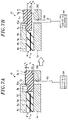
- FIGS. 7A and 7B explain still another exemplary flow of the process of measuring the thickness of the focus ring 5 .
- FIG. 7A shows a state where a jig 53 having a shape different from that of the jig 51 is mounted on the mounting surface 6 c .
- the jig 53 has a facing portion 53 a facing the upper surface of the focus ring 5 .
- the facing portion 53 a of the jig 53 is curved toward a boundary portion 5 c between the body portion 5 a and the protruding portion 5 b in a state where the jig 53 is mounted on the mounting surface 6 c .
- the boundary portion 5 c between the body portion 5 a and the protruding portion 5 b is easily damaged by plasma in the peripheral portion of the wafer W and is consumed more than other portions of the focus ring.
- FIG. 7A a state where the boundary portion 5 c is consumed is shown.
- the distance between the mounting surface 2 e and the mounting surface 6 c is “t 1 ”
- the distance between the mounting surface 6 c and the facing portion 53 a of the jig 53 mounted on the mounting surface 6 c is “t 2 ”. Therefore, “t 1 -t 2 ” is the gap dimension between the mounting surface 2 e and the facing portion 51 a of the jig 51 mounted on the mounting surface 6 c .
- the measurement unit 112 lifts the focus ring 5 until the upper surface of the focus ring 5 (i.e., the upper surface of the boundary portion 5 c ) becomes in contact with the facing portion 53 a of the jig 53 by lifting the lifter pins 63 using the elevating mechanisms 64 .
- FIG. 7B shows a state where the upper surface of the boundary portion 5 c is in contact with the facing portion 53 a of the jig 53 .
- the focus ring 5 is lifted from the mounting surface 2 e by “s 3 ”. As shown in FIG.
- the measurement unit 112 measures the lifted distance “s 3 ” of the focus ring 5 from the mounting surface 2 e when the upper surface of the boundary portion 5 c is in contact with the facing portion 53 a of the jig 53 . Then, in the plasma processing apparatus 10 , the thickness calculation unit 113 calculates a thickness “t b ” of the boundary portion 5 c by subtracting the measured lifted distance “s 3 ” of the focus ring 5 from the gap dimension “t 1 -t 2 ”.
- the plasma processing apparatus 10 can highly accurately measure the thickness of the boundary portion 5 c with a simple configuration in which the focus ring 5 is lifted until the upper surface of the boundary portion 5 c becomes in contact with the facing portion 53 a of the jig 53 mounted on the mounting surface 6 c.
- the plasma processing apparatus 10 includes the mounting table 2 , the elevating mechanisms 64 , the acquisition unit 111 , the measurement unit 112 , and the thickness calculation unit 113 .
- the mounting table 2 has the mounting surface 6 c on which the wafer W or the jig 51 used for measuring a thickness of the focus ring 5 is mounted and the mounting surface 2 e on which the focus ring 5 is mounted, the jig 51 having the facing portion 51 a facing the upper surface of the focus ring 5 .
- the elevating mechanisms 64 lift or lower the focus ring 5 with respect to the mounting surface 2 e .
- the acquisition unit 111 acquires the gap information 131 indicating the gap dimension between the mounting surface 2 e and the facing portion 51 a of the jig 51 mounted on the mounting surface 6 c .
- the measurement unit 112 lifts the focus ring 5 using the elevating mechanisms 64 in a state where the jig 51 is mounted on the mounting surface 6 c and measures the lifted distance of the focus ring 5 from the mounting surface 2 e when the upper surface of the focus ring 5 is in contact with the facing portion 51 a of the jig 51 .
- the thickness calculation unit 113 calculates the thickness of the focus ring 5 based on the gap dimension indicated by the acquired gap information 131 and the measured lifted distance of the focus ring 5 . Accordingly, the plasma processing apparatus 10 can highly accurately measure the thickness of the focus ring 5 with a simple configuration.
- the gap dimension is predetermined based on the distance between the mounting surface 2 e and the mounting surface 6 c and the distance between the mounting surface 6 c and the facing portion 51 a of the jig 51 mounted on the mounting surface 6 c . Accordingly, the plasma processing apparatus 10 can highly accurately measure the thickness of the focus ring 5 even when the mounting table 2 or the jig 51 has dimensional errors.
- the mounting table 2 is provided with the jig 51 mounted on the mounting surface 6 c or the electrostatic chuck 6 for attracting and holding the wafer W.
- the measurement unit 112 lifts the focus ring 5 using the elevating mechanism 64 in a state where the jig 51 is mounted on the mounting surface 6 c and attracted and held by the electrostatic chuck 6 . Accordingly, the plasma processing apparatus 10 can prevent the jig 51 from being separated from the mounting surface 6 c when the upper surface of the focus ring 5 becomes in contact with the facing portion 51 a of the jig 51 , which makes it possible to highly accurately measure the thickness of the focus ring 5 .
- the elevating mechanisms 64 are provided at multiple locations in the circumferential direction of the focus ring 5 .
- the measurement unit 112 lifts the focus ring 5 using the elevating mechanisms 64 arranged at multiple locations in the circumferential direction of the focus ring 5 .
- the measurement unit 112 measures the lifted distance of the focus ring 5 from the mounting surface 2 e at the multiple locations in the circumferential direction of the focus ring 5 when the upper surface of the focus ring 5 is in contact with the facing portion 51 a of the jig 51 .
- the thickness calculation unit 113 calculates the thickness of the focus ring 5 at the multiple locations in the circumferential direction of the focus ring 5 based on the gap dimension indicated by the acquired gap information and the measured lifted distance of the focus ring 5 . Accordingly, the plasma processing apparatus 10 can highly accurately measure the thickness of the focus ring 5 at the multiple locations in the circumferential direction of the focus ring 5 .
- the plasma processing apparatus 10 further includes an elevation control unit 114 for individually controlling the elevating mechanisms 64 such that the upper surface of the focus ring 5 is maintained at a given height based on the calculated thickness of the focus ring 5 . Therefore, in the plasma processing apparatus 10 , the upper surface of the focus ring 5 can be aligned with the upper surface of the wafer W in the circumferential direction. Accordingly, the plasma processing apparatus 10 can maintain the uniformity of the etching characteristics in the circumferential direction.
- the plasma processing apparatus 10 further includes the alerting unit 115 for performing alerting based on the calculated thickness of the focus ring 5 . Accordingly, the plasma processing apparatus 10 can notify the abnormality when the thickness of the focus ring 5 is reduced and the replacement of the focus ring 5 is required.
- the plasma processing apparatus 10 according to the second embodiment has the same configuration as that of the plasma processing apparatus 10 according to the first embodiment shown in FIGS. 1 and 2 . Therefore, redundant description thereof will be omitted.
- FIG. 8 is a block diagram showing a schematic configuration of the control unit 100 for controlling the plasma processing apparatus 10 according to the second embodiment.
- the control unit 100 according to the second embodiment has substantially the same configuration as that of the control unit 100 according to the first embodiment shown in FIG. 3 . Therefore, like reference numerals will be used for like parts, and redundant description thereof will be omitted.
- the process controller 110 includes a height calculation unit 121 and an elevation control unit 122 , instead of the elevation control unit 114 shown in FIG. 3 .
- the height calculation unit 121 calculates the height of the ring 5 at which the positional relationship between the upper surface of the wafer W and the upper surface of the focus ring 5 satisfies a predetermined gap based on the thickness of the focus ring 5 calculated by the thickness calculation unit 113 .
- the conditions for the positional relationship between the upper surface of the wafer W and the upper surface of the focus ring 5 which allows the angle of the hole formed in the wafer W by etching to be within a given allowable range are previously obtained by performing a test or the like.
- the conditions for the positional relationship between the upper surface of the wafer W and the upper surface of the focus ring 5 may be stored as condition information in the storage unit 130 .
- the height calculation unit 121 may read out the conditions for the positional relationship from the condition information. Further, the conditions for the positional relationship between the upper surface of the wafer W and the upper surface of the focus ring 5 may be determined depending on etching conditions such as an etching gas, a material of the wafer W, and the like, and stored as the condition information. The height calculation unit 21 may read out the conditions for the positional relationship corresponding to the etching conditions to be applied from the condition information. In the present embodiment, when the height of the upper surface of the wafer W is equal to the height of the upper surface of the focus ring 5 , the angle of the hole formed in the wafer W by etching is within the allowable range.
- the height calculation unit 121 calculates the height of the focus ring 5 at which the height of the upper surface of the wafer W becomes equal to the height of the upper surface of the focus ring 5 . Further, the height calculation unit 121 calculates the height of the focus ring 5 at which the height of the upper surface of the wafer W becomes equal to the height of the upper surface of the focus ring 5 at the multiple locations in the circumferential direction of the wafer W where the elevating mechanisms 64 are disposed.
- the elevation control unit 122 controls the elevating mechanisms 64 to lift or lower the lifter pins 64 to the height calculated by the height calculating unit 121 , thereby lifting or lowering the focus ring 5 .
- the elevation control unit 122 controls the elevating mechanisms 64 to lift or lower the focus ring 5 to the height calculated by the height calculation unit 121 at the locations where the elevating mechanisms 64 are disposed.
- the plasma processing apparatus 10 includes the height calculation unit 121 and the elevation control unit 122 .
- the height calculation unit 121 calculates the height of the focus ring 5 at which the positional relationship between the upper surface of the wafer W and the upper surface of the focus ring 5 satisfies a predetermined gap based on the calculated thickness of the focus ring 5 .
- the elevation control unit 122 controls the elevating mechanisms 64 such that the focus ring 5 reaches the calculated height. Therefore, in the plasma processing apparatus 10 , the upper surface of the focus ring 5 can be aligned with the upper surface of the wafer W in the circumferential direction. Accordingly, the plasma processing apparatus 10 can maintain the uniformity of the etching characteristics in the circumferential direction.
- the present disclosure can be variously modified without being limited to the above-described embodiments.
- the above-described plasma processing apparatus 10 is a capacitively coupled plasma processing apparatus 10 .
- the plasma processing apparatus 10 may be any type of plasma processing apparatus 10 such as an inductively coupled plasma processing apparatus 10 or a plasma processing apparatus 10 for exciting a gas by surface waves such as microwaves.
- the case of measuring a thickness of the focus ring 5 disposed around the wafer W has been described as an example.
- the present disclosure is not limited thereto.
- a thickness of another ring member may be measured in the same manner as that used in the process of measuring a thickness of the focus ring 5 according to the above-described embodiments.
- the plasma processing apparatus 10 may measure the gap dimension between the mounting surface 2 e on which the focus ring 5 is not mounted and the facing portion 51 a of the jig 51 mounted on the mounting surface 6 c using the jig 51 mounted on the mounting surface 6 c .
- the lifter pins 63 are lifted by the elevating mechanisms 64 in a state where the focus ring 5 is not mounted on the mounting surface 2 e and the jig 51 is mounted on the mounting surface 6 c and attracted and held by the electrostatic chuck 6 .
- the tip ends of the lifter pins 63 are in contact with the facing portion 51 a of the jig 51 , the lifted distance “s 4 ” of the tip ends of the lifter pins 63 from the mounting surface 2 e is measured and the gap dimension between the mounting surface 2 e and the facing portion 51 a of the jig 51 mounted on the mounting surface 6 c is specified.
- FIGS. 9A and 9B explain exemplary flow of the process of measuring the gap dimension using the jig 51 .
- FIG. 9A shows a state where the focus ring 5 is not mounted on the mounting surface 2 e and the jig 51 is mounted on the mounting surface 6 c .
- the jig 51 is attracted and held by the electrostatic chuck 6 .
- the heights of the lifter pins 63 are adjusted such that the tip ends of the lifter pins 63 are positioned on the same plane as the mounting surface 2 e .
- the lifter pins 63 are lifted by the elevating mechanisms 64 until the tip ends of the lifter pins 63 become in contact with the facing portion 51 a of the jig 51 .
- FIG. 9A shows a state where the focus ring 5 is not mounted on the mounting surface 2 e and the jig 51 is mounted on the mounting surface 6 c .
- the jig 51 is attracted and held by the electrostatic chuck 6 .
- FIG. 9B shows a state where the tip ends of the lifter pins 63 are in contact with the facing portion 51 a of the jig 51 .
- the tip ends of the lifter pins 63 are lifted from the mounting surface 2 e by “s 4 ”.
- the plasma processing apparatus 10 measures the lifted distance “s 4 ” of the tip ends of the lifter pins 63 from the mounting surface 2 e when the tip ends of the lifter pins 63 are in contact with the facing portion 51 a of the jig 51 .
- the lifted distance “s 4 ” is measured as the gap dimension “t 1 +t 2 ” between the mounting surface 2 e and the facing portion 51 a of the jig 51 mounted on the mounting surface 6 c .
- the accurate gap dimension can be obtained even when the actual dimensions of the mounting table 2 change due to thermal expansion or contraction caused by heating or cooling the mounting table 2 .
Landscapes
- Physics & Mathematics (AREA)
- Engineering & Computer Science (AREA)
- Plasma & Fusion (AREA)
- Chemical & Material Sciences (AREA)
- Analytical Chemistry (AREA)
- Electromagnetism (AREA)
- Spectroscopy & Molecular Physics (AREA)
- General Physics & Mathematics (AREA)
- Drying Of Semiconductors (AREA)
- Plasma Technology (AREA)
- Container, Conveyance, Adherence, Positioning, Of Wafer (AREA)
Abstract
Description
Claims (18)
Applications Claiming Priority (3)
| Application Number | Priority Date | Filing Date | Title |
|---|---|---|---|
| JPJP2018-188372 | 2018-10-03 | ||
| JP2018188372A JP7076351B2 (en) | 2018-10-03 | 2018-10-03 | Plasma processing device and ring member thickness measurement method |
| JP2018-188372 | 2018-10-03 |
Publications (2)
| Publication Number | Publication Date |
|---|---|
| US20200111648A1 US20200111648A1 (en) | 2020-04-09 |
| US11315766B2 true US11315766B2 (en) | 2022-04-26 |
Family
ID=70052467
Family Applications (1)
| Application Number | Title | Priority Date | Filing Date |
|---|---|---|---|
| US16/590,953 Active 2040-02-27 US11315766B2 (en) | 2018-10-03 | 2019-10-02 | Plasma processing apparatus and method for measuring thickness of ring member |
Country Status (5)
| Country | Link |
|---|---|
| US (1) | US11315766B2 (en) |
| JP (1) | JP7076351B2 (en) |
| KR (1) | KR102676476B1 (en) |
| CN (1) | CN110993477B (en) |
| TW (1) | TWI816890B (en) |
Families Citing this family (6)
| Publication number | Priority date | Publication date | Assignee | Title |
|---|---|---|---|---|
| JP2020087969A (en) * | 2018-11-15 | 2020-06-04 | 東京エレクトロン株式会社 | Plasma processing apparatus and ring member shape measuring method |
| JP7394601B2 (en) * | 2019-11-28 | 2023-12-08 | 東京エレクトロン株式会社 | Plasma processing equipment and measurement method |
| JP7783180B2 (en) * | 2020-08-25 | 2025-12-09 | 日清紡ケミカル株式会社 | Water-based resin crosslinking agent, water-based resin crosslinking agent-containing liquid, and water-based resin composition |
| KR102585286B1 (en) * | 2020-10-15 | 2023-10-05 | 세메스 주식회사 | Apparatus for treating substrate and mesuring method of consumable component |
| WO2022163582A1 (en) * | 2021-01-29 | 2022-08-04 | 東京エレクトロン株式会社 | Plasma processing device |
| JP7616941B2 (en) * | 2021-05-11 | 2025-01-17 | 東京エレクトロン株式会社 | SUBSTRATE PROCESSING SYSTEM AND METHOD FOR ESTIMATING HEIGHT OF ANNULAR MEMBER |
Citations (9)
| Publication number | Priority date | Publication date | Assignee | Title |
|---|---|---|---|---|
| JP2002176030A (en) | 2000-12-07 | 2002-06-21 | Semiconductor Leading Edge Technologies Inc | Plasma etching apparatus and plasma etching method |
| US20050061447A1 (en) * | 2003-09-19 | 2005-03-24 | Samsung Electronics Co., Ltd. | Plasma etching apparatus |
| JP2010199526A (en) | 2009-02-02 | 2010-09-09 | Tokyo Electron Ltd | Plasma processing apparatus, and method and apparatus for measuring temperature |
| JP2016146472A (en) | 2015-01-16 | 2016-08-12 | ラム リサーチ コーポレーションLam Research Corporation | Movable edge coupling ring for edge processing control during semiconductor wafer processing |
| US20170287682A1 (en) * | 2016-03-29 | 2017-10-05 | Lam Research Corporation | Systems and methods for performing edge ring characterization |
| US20170363407A1 (en) * | 2016-06-20 | 2017-12-21 | Tokyo Electron Limited | Measuring instrument for measuring electrostatic capacity and method of calibrating transfer position data in processing system by using measuring instrument |
| US20200161101A1 (en) * | 2018-11-15 | 2020-05-21 | Tokyo Electron Limited | Plasma processing apparatus and method for measuring shape of ring member |
| US20200234929A1 (en) * | 2019-01-17 | 2020-07-23 | Tokyo Electron Limited | Plasma processing apparatus and method for measuring misalignment of ring member |
| US20200411390A1 (en) * | 2019-06-26 | 2020-12-31 | Samsung Electronics Co., Ltd. | Sensor device and etching apparatus having the same |
Family Cites Families (8)
| Publication number | Priority date | Publication date | Assignee | Title |
|---|---|---|---|---|
| JP2001230239A (en) | 2000-02-15 | 2001-08-24 | Tokyo Electron Ltd | Processing device and processing method |
| KR100783062B1 (en) * | 2006-12-27 | 2007-12-07 | 세메스 주식회사 | Substrate Supporting Device, Plasma Etching Device and Plasma Etching Method |
| JP2013030693A (en) | 2011-07-29 | 2013-02-07 | Hitachi High-Technologies Corp | Plasma processing apparatus |
| JP6383647B2 (en) | 2014-11-19 | 2018-08-29 | 東京エレクトロン株式会社 | Measuring system and measuring method |
| US10651015B2 (en) * | 2016-02-12 | 2020-05-12 | Lam Research Corporation | Variable depth edge ring for etch uniformity control |
| JP2018032721A (en) * | 2016-08-24 | 2018-03-01 | 東京エレクトロン株式会社 | Maintenance method of plasma processing device |
| JP6812224B2 (en) * | 2016-12-08 | 2021-01-13 | 東京エレクトロン株式会社 | Board processing equipment and mounting table |
| US10553404B2 (en) * | 2017-02-01 | 2020-02-04 | Applied Materials, Inc. | Adjustable extended electrode for edge uniformity control |
-
2018
- 2018-10-03 JP JP2018188372A patent/JP7076351B2/en active Active
-
2019
- 2019-09-26 TW TW108134753A patent/TWI816890B/en active
- 2019-09-29 CN CN201910932470.4A patent/CN110993477B/en active Active
- 2019-09-30 KR KR1020190120983A patent/KR102676476B1/en active Active
- 2019-10-02 US US16/590,953 patent/US11315766B2/en active Active
Patent Citations (9)
| Publication number | Priority date | Publication date | Assignee | Title |
|---|---|---|---|---|
| JP2002176030A (en) | 2000-12-07 | 2002-06-21 | Semiconductor Leading Edge Technologies Inc | Plasma etching apparatus and plasma etching method |
| US20050061447A1 (en) * | 2003-09-19 | 2005-03-24 | Samsung Electronics Co., Ltd. | Plasma etching apparatus |
| JP2010199526A (en) | 2009-02-02 | 2010-09-09 | Tokyo Electron Ltd | Plasma processing apparatus, and method and apparatus for measuring temperature |
| JP2016146472A (en) | 2015-01-16 | 2016-08-12 | ラム リサーチ コーポレーションLam Research Corporation | Movable edge coupling ring for edge processing control during semiconductor wafer processing |
| US20170287682A1 (en) * | 2016-03-29 | 2017-10-05 | Lam Research Corporation | Systems and methods for performing edge ring characterization |
| US20170363407A1 (en) * | 2016-06-20 | 2017-12-21 | Tokyo Electron Limited | Measuring instrument for measuring electrostatic capacity and method of calibrating transfer position data in processing system by using measuring instrument |
| US20200161101A1 (en) * | 2018-11-15 | 2020-05-21 | Tokyo Electron Limited | Plasma processing apparatus and method for measuring shape of ring member |
| US20200234929A1 (en) * | 2019-01-17 | 2020-07-23 | Tokyo Electron Limited | Plasma processing apparatus and method for measuring misalignment of ring member |
| US20200411390A1 (en) * | 2019-06-26 | 2020-12-31 | Samsung Electronics Co., Ltd. | Sensor device and etching apparatus having the same |
Also Published As
| Publication number | Publication date |
|---|---|
| US20200111648A1 (en) | 2020-04-09 |
| JP2020057712A (en) | 2020-04-09 |
| KR20200038417A (en) | 2020-04-13 |
| TWI816890B (en) | 2023-10-01 |
| TW202029333A (en) | 2020-08-01 |
| JP7076351B2 (en) | 2022-05-27 |
| CN110993477B (en) | 2024-07-30 |
| CN110993477A (en) | 2020-04-10 |
| KR102676476B1 (en) | 2024-06-18 |
Similar Documents
| Publication | Publication Date | Title |
|---|---|---|
| US11315766B2 (en) | Plasma processing apparatus and method for measuring thickness of ring member | |
| US12315704B2 (en) | Plasma processing apparatus, and method and program for controlling elevation of focus ring | |
| JP7055054B2 (en) | Plasma processing equipment, plasma control method, and plasma control program | |
| US10186402B2 (en) | Measurement system and measurement method | |
| US12300469B2 (en) | Plasma processing apparatus, calculation method, and calculation program | |
| US20190198298A1 (en) | Plasma etching apparatus and plasma etching method | |
| US10825662B2 (en) | Method for driving member and processing apparatus | |
| US10375763B2 (en) | Temperature control apparatus, temperature control method and recording medium | |
| US20190304824A1 (en) | Plasma processing apparatus and method of transferring workpiece | |
| US20200234929A1 (en) | Plasma processing apparatus and method for measuring misalignment of ring member | |
| US20200161101A1 (en) | Plasma processing apparatus and method for measuring shape of ring member | |
| JP2025013179A (en) | Substrate processing apparatus | |
| WO2024171911A1 (en) | Substrate processing device and substrate processing method |
Legal Events
| Date | Code | Title | Description |
|---|---|---|---|
| AS | Assignment |
Owner name: TOKYO ELECTRON LIMITED, JAPAN Free format text: ASSIGNMENT OF ASSIGNORS INTEREST;ASSIGNOR:OGATA, ATSUSHI;REEL/FRAME:050604/0372 Effective date: 20190926 |
|
| FEPP | Fee payment procedure |
Free format text: ENTITY STATUS SET TO UNDISCOUNTED (ORIGINAL EVENT CODE: BIG.); ENTITY STATUS OF PATENT OWNER: LARGE ENTITY |
|
| STPP | Information on status: patent application and granting procedure in general |
Free format text: DOCKETED NEW CASE - READY FOR EXAMINATION |
|
| STPP | Information on status: patent application and granting procedure in general |
Free format text: NON FINAL ACTION MAILED |
|
| STPP | Information on status: patent application and granting procedure in general |
Free format text: RESPONSE TO NON-FINAL OFFICE ACTION ENTERED AND FORWARDED TO EXAMINER |
|
| STPP | Information on status: patent application and granting procedure in general |
Free format text: NOTICE OF ALLOWANCE MAILED -- APPLICATION RECEIVED IN OFFICE OF PUBLICATIONS |
|
| STPP | Information on status: patent application and granting procedure in general |
Free format text: PUBLICATIONS -- ISSUE FEE PAYMENT VERIFIED |
|
| STCF | Information on status: patent grant |
Free format text: PATENTED CASE |
|
| MAFP | Maintenance fee payment |
Free format text: PAYMENT OF MAINTENANCE FEE, 4TH YEAR, LARGE ENTITY (ORIGINAL EVENT CODE: M1551); ENTITY STATUS OF PATENT OWNER: LARGE ENTITY Year of fee payment: 4 |