US11315744B2 - Electric storage device - Google Patents
Electric storage device Download PDFInfo
- Publication number
- US11315744B2 US11315744B2 US16/186,885 US201816186885A US11315744B2 US 11315744 B2 US11315744 B2 US 11315744B2 US 201816186885 A US201816186885 A US 201816186885A US 11315744 B2 US11315744 B2 US 11315744B2
- Authority
- US
- United States
- Prior art keywords
- electrode
- storage device
- elastic
- electric storage
- leading end
- Prior art date
- Legal status (The legal status is an assumption and is not a legal conclusion. Google has not performed a legal analysis and makes no representation as to the accuracy of the status listed.)
- Active, expires
Links
Images


Classifications
-
- H—ELECTRICITY
- H01—ELECTRIC ELEMENTS
- H01G—CAPACITORS; CAPACITORS, RECTIFIERS, DETECTORS, SWITCHING DEVICES, LIGHT-SENSITIVE OR TEMPERATURE-SENSITIVE DEVICES OF THE ELECTROLYTIC TYPE
- H01G11/00—Hybrid capacitors, i.e. capacitors having different positive and negative electrodes; Electric double-layer [EDL] capacitors; Processes for the manufacture thereof or of parts thereof
- H01G11/78—Cases; Housings; Encapsulations; Mountings
-
- H—ELECTRICITY
- H01—ELECTRIC ELEMENTS
- H01G—CAPACITORS; CAPACITORS, RECTIFIERS, DETECTORS, SWITCHING DEVICES, LIGHT-SENSITIVE OR TEMPERATURE-SENSITIVE DEVICES OF THE ELECTROLYTIC TYPE
- H01G11/00—Hybrid capacitors, i.e. capacitors having different positive and negative electrodes; Electric double-layer [EDL] capacitors; Processes for the manufacture thereof or of parts thereof
- H01G11/22—Electrodes
- H01G11/26—Electrodes characterised by their structure, e.g. multi-layered, porosity or surface features
-
- H—ELECTRICITY
- H01—ELECTRIC ELEMENTS
- H01G—CAPACITORS; CAPACITORS, RECTIFIERS, DETECTORS, SWITCHING DEVICES, LIGHT-SENSITIVE OR TEMPERATURE-SENSITIVE DEVICES OF THE ELECTROLYTIC TYPE
- H01G11/00—Hybrid capacitors, i.e. capacitors having different positive and negative electrodes; Electric double-layer [EDL] capacitors; Processes for the manufacture thereof or of parts thereof
- H01G11/52—Separators
-
- H—ELECTRICITY
- H01—ELECTRIC ELEMENTS
- H01G—CAPACITORS; CAPACITORS, RECTIFIERS, DETECTORS, SWITCHING DEVICES, LIGHT-SENSITIVE OR TEMPERATURE-SENSITIVE DEVICES OF THE ELECTROLYTIC TYPE
- H01G11/00—Hybrid capacitors, i.e. capacitors having different positive and negative electrodes; Electric double-layer [EDL] capacitors; Processes for the manufacture thereof or of parts thereof
- H01G11/54—Electrolytes
- H01G11/58—Liquid electrolytes
-
- H—ELECTRICITY
- H01—ELECTRIC ELEMENTS
- H01G—CAPACITORS; CAPACITORS, RECTIFIERS, DETECTORS, SWITCHING DEVICES, LIGHT-SENSITIVE OR TEMPERATURE-SENSITIVE DEVICES OF THE ELECTROLYTIC TYPE
- H01G11/00—Hybrid capacitors, i.e. capacitors having different positive and negative electrodes; Electric double-layer [EDL] capacitors; Processes for the manufacture thereof or of parts thereof
- H01G11/66—Current collectors
- H01G11/72—Current collectors specially adapted for integration in multiple or stacked hybrid or EDL capacitors
-
- H—ELECTRICITY
- H01—ELECTRIC ELEMENTS
- H01G—CAPACITORS; CAPACITORS, RECTIFIERS, DETECTORS, SWITCHING DEVICES, LIGHT-SENSITIVE OR TEMPERATURE-SENSITIVE DEVICES OF THE ELECTROLYTIC TYPE
- H01G11/00—Hybrid capacitors, i.e. capacitors having different positive and negative electrodes; Electric double-layer [EDL] capacitors; Processes for the manufacture thereof or of parts thereof
- H01G11/74—Terminals, e.g. extensions of current collectors
- H01G11/76—Terminals, e.g. extensions of current collectors specially adapted for integration in multiple or stacked hybrid or EDL capacitors
-
- H—ELECTRICITY
- H01—ELECTRIC ELEMENTS
- H01M—PROCESSES OR MEANS, e.g. BATTERIES, FOR THE DIRECT CONVERSION OF CHEMICAL ENERGY INTO ELECTRICAL ENERGY
- H01M10/00—Secondary cells; Manufacture thereof
- H01M10/04—Construction or manufacture in general
-
- H—ELECTRICITY
- H01—ELECTRIC ELEMENTS
- H01M—PROCESSES OR MEANS, e.g. BATTERIES, FOR THE DIRECT CONVERSION OF CHEMICAL ENERGY INTO ELECTRICAL ENERGY
- H01M10/00—Secondary cells; Manufacture thereof
- H01M10/04—Construction or manufacture in general
- H01M10/0436—Small-sized flat cells or batteries for portable equipment
-
- H—ELECTRICITY
- H01—ELECTRIC ELEMENTS
- H01M—PROCESSES OR MEANS, e.g. BATTERIES, FOR THE DIRECT CONVERSION OF CHEMICAL ENERGY INTO ELECTRICAL ENERGY
- H01M50/00—Constructional details or processes of manufacture of the non-active parts of electrochemical cells other than fuel cells, e.g. hybrid cells
- H01M50/10—Primary casings; Jackets or wrappings
- H01M50/102—Primary casings; Jackets or wrappings characterised by their shape or physical structure
- H01M50/103—Primary casings; Jackets or wrappings characterised by their shape or physical structure prismatic or rectangular
-
- H—ELECTRICITY
- H01—ELECTRIC ELEMENTS
- H01M—PROCESSES OR MEANS, e.g. BATTERIES, FOR THE DIRECT CONVERSION OF CHEMICAL ENERGY INTO ELECTRICAL ENERGY
- H01M50/00—Constructional details or processes of manufacture of the non-active parts of electrochemical cells other than fuel cells, e.g. hybrid cells
- H01M50/10—Primary casings; Jackets or wrappings
- H01M50/116—Primary casings; Jackets or wrappings characterised by the material
-
- H—ELECTRICITY
- H01—ELECTRIC ELEMENTS
- H01M—PROCESSES OR MEANS, e.g. BATTERIES, FOR THE DIRECT CONVERSION OF CHEMICAL ENERGY INTO ELECTRICAL ENERGY
- H01M50/00—Constructional details or processes of manufacture of the non-active parts of electrochemical cells other than fuel cells, e.g. hybrid cells
- H01M50/10—Primary casings; Jackets or wrappings
- H01M50/172—Arrangements of electric connectors penetrating the casing
- H01M50/174—Arrangements of electric connectors penetrating the casing adapted for the shape of the cells
- H01M50/176—Arrangements of electric connectors penetrating the casing adapted for the shape of the cells for prismatic or rectangular cells
-
- H—ELECTRICITY
- H01—ELECTRIC ELEMENTS
- H01M—PROCESSES OR MEANS, e.g. BATTERIES, FOR THE DIRECT CONVERSION OF CHEMICAL ENERGY INTO ELECTRICAL ENERGY
- H01M50/00—Constructional details or processes of manufacture of the non-active parts of electrochemical cells other than fuel cells, e.g. hybrid cells
- H01M50/50—Current conducting connections for cells or batteries
- H01M50/531—Electrode connections inside a battery casing
- H01M50/533—Electrode connections inside a battery casing characterised by the shape of the leads or tabs
-
- H—ELECTRICITY
- H01—ELECTRIC ELEMENTS
- H01M—PROCESSES OR MEANS, e.g. BATTERIES, FOR THE DIRECT CONVERSION OF CHEMICAL ENERGY INTO ELECTRICAL ENERGY
- H01M50/00—Constructional details or processes of manufacture of the non-active parts of electrochemical cells other than fuel cells, e.g. hybrid cells
- H01M50/50—Current conducting connections for cells or batteries
- H01M50/543—Terminals
- H01M50/547—Terminals characterised by the disposition of the terminals on the cells
- H01M50/55—Terminals characterised by the disposition of the terminals on the cells on the same side of the cell
-
- H—ELECTRICITY
- H01—ELECTRIC ELEMENTS
- H01G—CAPACITORS; CAPACITORS, RECTIFIERS, DETECTORS, SWITCHING DEVICES, LIGHT-SENSITIVE OR TEMPERATURE-SENSITIVE DEVICES OF THE ELECTROLYTIC TYPE
- H01G11/00—Hybrid capacitors, i.e. capacitors having different positive and negative electrodes; Electric double-layer [EDL] capacitors; Processes for the manufacture thereof or of parts thereof
- H01G11/66—Current collectors
-
- H—ELECTRICITY
- H01—ELECTRIC ELEMENTS
- H01G—CAPACITORS; CAPACITORS, RECTIFIERS, DETECTORS, SWITCHING DEVICES, LIGHT-SENSITIVE OR TEMPERATURE-SENSITIVE DEVICES OF THE ELECTROLYTIC TYPE
- H01G11/00—Hybrid capacitors, i.e. capacitors having different positive and negative electrodes; Electric double-layer [EDL] capacitors; Processes for the manufacture thereof or of parts thereof
- H01G11/74—Terminals, e.g. extensions of current collectors
-
- H—ELECTRICITY
- H01—ELECTRIC ELEMENTS
- H01M—PROCESSES OR MEANS, e.g. BATTERIES, FOR THE DIRECT CONVERSION OF CHEMICAL ENERGY INTO ELECTRICAL ENERGY
- H01M10/00—Secondary cells; Manufacture thereof
- H01M10/05—Accumulators with non-aqueous electrolyte
- H01M10/058—Construction or manufacture
-
- H—ELECTRICITY
- H01—ELECTRIC ELEMENTS
- H01M—PROCESSES OR MEANS, e.g. BATTERIES, FOR THE DIRECT CONVERSION OF CHEMICAL ENERGY INTO ELECTRICAL ENERGY
- H01M2220/00—Batteries for particular applications
- H01M2220/30—Batteries in portable systems, e.g. mobile phone, laptop
-
- H—ELECTRICITY
- H01—ELECTRIC ELEMENTS
- H01M—PROCESSES OR MEANS, e.g. BATTERIES, FOR THE DIRECT CONVERSION OF CHEMICAL ENERGY INTO ELECTRICAL ENERGY
- H01M50/00—Constructional details or processes of manufacture of the non-active parts of electrochemical cells other than fuel cells, e.g. hybrid cells
- H01M50/10—Primary casings; Jackets or wrappings
- H01M50/116—Primary casings; Jackets or wrappings characterised by the material
- H01M50/117—Inorganic material
- H01M50/119—Metals
-
- H—ELECTRICITY
- H01—ELECTRIC ELEMENTS
- H01M—PROCESSES OR MEANS, e.g. BATTERIES, FOR THE DIRECT CONVERSION OF CHEMICAL ENERGY INTO ELECTRICAL ENERGY
- H01M50/00—Constructional details or processes of manufacture of the non-active parts of electrochemical cells other than fuel cells, e.g. hybrid cells
- H01M50/10—Primary casings; Jackets or wrappings
- H01M50/116—Primary casings; Jackets or wrappings characterised by the material
- H01M50/121—Organic material
-
- Y—GENERAL TAGGING OF NEW TECHNOLOGICAL DEVELOPMENTS; GENERAL TAGGING OF CROSS-SECTIONAL TECHNOLOGIES SPANNING OVER SEVERAL SECTIONS OF THE IPC; TECHNICAL SUBJECTS COVERED BY FORMER USPC CROSS-REFERENCE ART COLLECTIONS [XRACs] AND DIGESTS
- Y02—TECHNOLOGIES OR APPLICATIONS FOR MITIGATION OR ADAPTATION AGAINST CLIMATE CHANGE
- Y02E—REDUCTION OF GREENHOUSE GAS [GHG] EMISSIONS, RELATED TO ENERGY GENERATION, TRANSMISSION OR DISTRIBUTION
- Y02E60/00—Enabling technologies; Technologies with a potential or indirect contribution to GHG emissions mitigation
- Y02E60/10—Energy storage using batteries
-
- Y—GENERAL TAGGING OF NEW TECHNOLOGICAL DEVELOPMENTS; GENERAL TAGGING OF CROSS-SECTIONAL TECHNOLOGIES SPANNING OVER SEVERAL SECTIONS OF THE IPC; TECHNICAL SUBJECTS COVERED BY FORMER USPC CROSS-REFERENCE ART COLLECTIONS [XRACs] AND DIGESTS
- Y02—TECHNOLOGIES OR APPLICATIONS FOR MITIGATION OR ADAPTATION AGAINST CLIMATE CHANGE
- Y02P—CLIMATE CHANGE MITIGATION TECHNOLOGIES IN THE PRODUCTION OR PROCESSING OF GOODS
- Y02P70/00—Climate change mitigation technologies in the production process for final industrial or consumer products
- Y02P70/50—Manufacturing or production processes characterised by the final manufactured product
Definitions
- the present invention relates to an electric storage device.
- Patent Document 1 discloses a battery including an electrode body obtained by laminating and winding a positive electrode, a separator, and a negative electrode.
- an installation space which does not have a rectangular shape in plan view can be used as an installation space for an electrical storage device in the electronic device. For this reason, an electrical storage device not having a rectangular shape in plan view is desired.
- Impact resistance is also required for the electric storage device.
- an electric storage device includes a case having a substantially rectangular shape including a cutout part.
- An electrode body is disposed in the case and includes a first electrode, a second electrode, and a separator disposed between the first and second electrodes.
- An electrolyte is located in the case and at least partially impregnates the electrode body.
- a first electrode terminal is located on a first part of a side surface of the case and is electrically connected to the first electrode by a first connection member which has elasticity in a direction extending from the first electrode terminal to the first electrode.
- a second electrode terminal is located on a second part of the side surface of the case and is electrically connected to the second electrode by a second elastic connection member which has elasticity in a direction extending from the second electrode terminal to the second electrode.
- the positive and negative electrode terminals are each provided on respective parts of the side surface of the case which do not form part of the cutout part.
- a virtual straight line connecting a center of the first electrode terminal and a center of the second electrode terminal does not overlap with the electrode body in plan view.
- the first electrode includes a first electrode body and a first extended part extending from the first electrode body and the second electrode includes a second electrode body facing and a second extended part extending from the second electrode body.
- the first and second electrode bodies face one another.
- the first connection member is constituted by a plate member including a first part connected to the first extended part, a second part connected to the first connection member, and a first bent part connecting the first and second parts.
- the second connection member is constituted by a plate member including a third part connected with the second extended part, a fourth part connected with the second connection member, and a second bent part connecting the third and fourth parts.
- the first electrode, the second electrode, and the separator are integrated in the electrode body and the electrode body and the case are physically joined together.
- the electrode body and the case are physically joined together by an adhesive layer bonding the electrode body and the case.
- the first and second electrode terminals are formed by the case.
- the present invention can provide an electric storage device not having a rectangular shape in plan view but having excellent impact resistance.
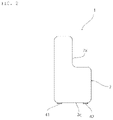
- FIG. 1 is a schematic perspective view of an electric storage device according to a first embodiment.
- FIG. 2 is a schematic plan view of the electric storage device according to the first embodiment.
- FIG. 3 is a schematic cross-sectional view taken along line III-III in FIG. 1 .
- FIG. 4 is a schematic plan view of part of the electric storage device according to the first embodiment.
- FIG. 5 is a schematic cross-sectional view taken along line V-V in FIG. 1 .
- FIG. 6 is a schematic cross-sectional view taken along line VI-VI in FIG. 1 .
- FIG. 7 is a schematic cross-sectional view for description of a method of manufacturing the electric storage device according to the first embodiment.
- FIG. 8 is a schematic cross-sectional view of an electric storage device according to a second embodiment.
- FIG. 9 is a schematic cross-sectional view of an electric storage device according to a third embodiment.
- FIG. 10 is a schematic cross-sectional view of part of an electric storage device according to a fourth embodiment.
- FIG. 11 is a schematic cross-sectional view of part of the electric storage device according to the fourth embodiment.
- An electric storage device 1 illustrated in FIGS. 1 to 4 includes an electrolyte 4 (see FIG. 3 ) such as electrolytic solution.
- the electric storage device 1 may be, for example, a battery such as a secondary battery, or a capacitor such as an electric double-layer capacitor.
- the electric storage device 1 includes a case 2 having a generally rectangular shape including a cutout part 2 a in plan view (i.e., as viewed in FIG. 2 ).
- a “rectangular shape including a cutout part” includes a rectangular shape including a cutout part and rounded corners.
- the cutout part 2 a also has a substantially rectangular shape in plan view (again, as viewed in FIG. 3 ). Specifically, a single cutout part 2 a having a substantially rectangular shape with rounded inner and outer corners is provided.
- the present invention is not limited to this configuration.
- the case may be provided with a plurality of cutout parts.
- a cutout part may be provided at each of a plurality of corners of the case.
- the shape of the cutout part provided to the case is not limited, too.
- the cutout part provided to the case may have, for example, an arcuate shape, a polygonal shape, or a shape that is a combination thereof.
- the case 2 may be made of a conductor or an insulator.
- the case 2 may, for example, be made of metal such as aluminum, stainless steel, or copper, or an insulator such as resin.
- an electrode body 3 is disposed inside the case 2 .
- the electrode body 3 includes a plurality of positive electrodes 31 , a plurality of negative electrodes 32 , and a plurality of separators 33 .
- Each positive electrode 31 faces an adjacent negative electrode 32 with a respective separator 33 located there between to form a positive/negative electrode pair.
- the separator 33 insulates the positive and negative electrodes 31 and 32 .
- each positive electrode 31 is surrounded by a pair of separators 33 (one located above the positive electrode 31 and one located below the positive electrode 31 ) and lateral side edges of those separators are connected with each other to form a separator bag 33 a with the positive electrode 31 disposed therein.
- separators which are adjacent to each other in the lamination direction T do not have to be joined into a bag shape.
- the present embodiment describes an example in which the electrode body 3 is a laminated electrode body obtained by laminating the plurality of sheet shaped positive electrodes 31 , the plurality of sheet shaped separators 33 , and the plurality of sheet shaped negative electrode 32 .
- the electrode body is not particularly limited as long as the electrode body has a configuration that allows the accumulation of electrical power.
- the electrode body may be achieved by a wound body obtained by winding a lamination sheet in which a plurality of positive/negative electrode pairs are provided, each positive/negative electrode pair including a respective positive electrode, a respective separator, and a respective negative electrode, all of which are laminated in the stated order.
- the configuration of the positive electrode 31 may be determined as appropriate in accordance with the type of the electric storage device 1 it is used in.
- the positive electrode 31 may include a positive electrode collector, and an active material layer provided on at least one surface of the positive electrode collector.
- the positive electrode 31 may include a positive electrode collector, and a polarizable electrode layer provided on at least one surface of the positive electrode collector.
- the configuration of the negative electrode 32 may similarly be determined as appropriate in accordance with the type of the electric storage device 1 it is used in.
- the negative electrode 32 may include a negative electrode collector, and an active material layer provided on at least one surface of the negative electrode collector.
- the negative electrode 32 may include a negative electrode collector and a polarizable electrode layer provided on at least one surface of the negative electrode collector.
- the separators 33 may be, for example, a porous sheet including open cells through which ions in an electrolyte are movable.
- the separators 33 may be made of, for example, polypropylene, polyethylene, polyimide, cellulose, aramid, polyvinylidene fluoride, or Teflon (registered trademark).
- the surface of the separators 33 may be covered by an inorganic particle coat layer, a bonding layer, or the like.
- the surface of the separators 33 may have a bonding property.
- the separators 33 may be a single-layer film made of one kind of material, or may be a composite film or multi-layered film made of one or two or more types of material.
- an insulation layer such as an inorganic particle coat layer may be provided on the surface of each of the positive electrode 31 and the negative electrode 32 .
- the insulator acts as the separator (and can be considered a separator for the purpose of the present invention.
- an undercoat layer containing, for example, carbon may be provided between the collector and the active material layer.
- each of the positive/negative electrode pairs comprises a respective positive electrode 31 , a respective separator 33 and a respective negative electrode 32 which are laminated together in the stated order.
- Each of the positive/negative electrode pairs are also laminated together to form a laminated body 70 .
- the outer lateral edges of the separators 33 are then adhered together (and, in the preferred embodiment) bent upwardly as viewed in FIG. 3 to form the integrated electrode body 3 .
- a first insulation tape 51 is provided on a W1 side (the left side as viewed in FIG.
- the laminated body 70 extends from the second main surface 70 b of the laminated body 70 , upwardly across the left lateral edge of the laminated body (so as to adhere the left lateral edges of the separators 33 to each other and to push them upwardly) and onto the first main surface 70 a of the laminated body 70 .
- at least a lateral leading end part of a first end part 33 e 1 of the separators 33 are held so that at least the leading end part of the first end part 33 e 1 is bent upwardly (more generally, toward one side (T1 side)) in the lamination direction T.
- a second insulation tape 52 is provided on a W2 side (the right side as viewed in FIG. 3 ) of the laminated body 70 and extends from the second main surface 70 b of the laminated body 70 , upwardly across the right lateral edge of the laminated body (so as to adhere the right lateral edges of the separators 33 to each other and to push them upwardly) and onto the first main surface 70 a of the laminated body 70 .
- a lateral leading end part of a second end part 33 e 2 of the separators 33 are held so that at least the leading end part of the second end part 33 e 2 is bent upwardly (more generally, toward one side (T1 side)) in the lamination direction T.
- the method of joining the insulation tapes 51 and 52 with the laminated body 70 is not particularly limited.
- the insulation tapes 51 and 52 may be joined with the laminated body 70 directly or by adhesive bonding using an adhesive bonding agent.
- the insulation tapes 51 and 52 may be formed of adhesive bonding tapes and bonded to the laminated body 70 .
- the insulation tapes 51 and 52 may be formed of double-sided adhesive bonding tapes and bonded to the laminated body 70 , and the laminated body 70 may be bonded and fixed to the case 2 through the insulation tapes 51 and 52 . This configuration effectively reduces displacement of the laminated body 70 in the case 2 .
- the insulation tapes 51 and 52 and the laminated body 70 may be fixed together by using an adhesive bonding tape different from the insulation tapes 51 and 52 .
- an adhesive bonding agent includes both an adhesive agent and a bonding agent.
- An adhesive bonding tape includes an adhesive tape and a bonding tape.
- the insulation tape 5 may be, for example, a tape made of resin such as polyimide, polypropylene, or acrylic, or metal foil such as aluminum foil, copper foil, stainless steel foil, or nickel foil, the surface of which is coated with an insulation layer.
- resin such as polyimide, polypropylene, or acrylic
- metal foil such as aluminum foil, copper foil, stainless steel foil, or nickel foil, the surface of which is coated with an insulation layer.
- the positive electrode 31 and the separator 33 may be bonded to each other through a bonding agent, and the negative electrode 32 and the separator 33 may be bonded to each other through a bonding agent.
- the electrode body 3 and the case 2 are joined together. Specifically, as illustrated in FIG. 3 , the electrode body 3 is bonded and fixed to an inner surface of the case 2 through a bonding layer 6 . In FIG. 3 , the electrode body 3 is joined on the upper side (T1 side) relative to the case 2 , but may also or alternatively be joined on the lower side. The electrode body 3 may also be joined to inner surfaces of the case 2 on both sides in the thickness direction T.
- each of the positive electrodes 31 includes a generally rectangular positive electrode body 31 a and a first extended part 31 b which extends from the positive electrode body 31 a in a length direction L.
- Each of the negative electrodes 32 includes a generally rectangular negative electrode body 32 a and a second extended part 32 b which extends from the negative electrode body 32 a in the length direction L. While this is preferred, the first and/or second extended parts may extended in directions other than the length direction L.
- a positive electrode terminal 41 is provided on a side surface 2 c of one side of the case 2 in the length direction L.
- the positive electrode terminal 41 is electrically connected with each of the first extended parts 31 b of the positive electrodes 31 .
- each of the first extended parts 31 b which are physically and electrically connected to one another, are bent such that their leading end part 31 b 1 extends upwardly (as viewed in FIG. 3 ) toward the T1 side along the lamination direction T.
- the leading end parts 31 b 1 are connected to the positive electrode terminal 41 through a first connection member 61 .
- the first connection member 61 includes a first part 61 a which is physically and electrically connected to the first extended parts 31 b 1 , a second part 61 b which is physically and electrically connected to the positive electrode terminal 41 and a first bent part 61 c which physically and electrically connects the first and second parts 61 a and 61 b and which protrudes upwardly (as viewed in FIG. 3 ) toward the T1 side.
- the first connection member 61 is preferably an elastic member made of, for example, metal. Accordingly, the first connection member 61 is elastic in the length direction L.
- a negative electrode terminal 42 is provided on the side surface 2 c of the case 2 .
- the negative electrode terminal 42 is electrically connected with the second extended parts 32 b which are physically and electrically connected to one another.
- each of the first extended parts 32 b are bent such that their leading end part 32 b 1 extends upwardly (as viewed in FIG. 3 ) toward the T1 side along the lamination direction T.
- the leading end parts 32 b 1 are connected to the negative electrode terminal 42 through a first connection member 62 .
- the second connection member 62 includes a third part 62 a which is electrically and physically connected with the second extended parts 32 b , a fourth part 62 b which is physically and electrically connected with the negative electrode terminal 42 , and a second bent part 62 c which physically and electrically connects the third part 62 a and to the fourth part 62 b and which protrudes toward the T1 side.
- the second connection member 62 is an elastic member made of, for example, metal. Accordingly, the second connection member 62 is elastic in the length direction L.
- the electric storage device 1 includes the first and second connection members 61 and 62 which are both elastic in the length direction L. With this configuration, when, for example, stress, impact, or vibration is applied to the electric storage device 1 , transfer of the stress or the like to the electrode body 3 is buffered by the first and second connection members 61 and 62 . Accordingly, the electric storage device 1 has excellent impact resistance.
- the electric storage device 1 has an excellent impact resistance.
- the electrode body 3 and the case 2 are bonded to each other through the bonding layer 6 . With this configuration, transfer of impact applied to the case 2 to the electrode body 3 is buffered by the bonding layer 6 . This further improves the impact resistance of the electric storage device 1 .
- the bonding layer 6 is preferably elastic, adhesive, or elastic and adhesive to achieve excellent impact resistance.
- the first and second connection members may be provided with a plurality of bent parts. However, when a plurality of bend parts are provided, the sizes of the first and second connection members tends to increase. For this reason, it is preferred that the first and second connection members and 62 are each provided with a single bent part 61 c and 62 c . With this configuration, the first and second connection members 61 and 62 are small-sized. Thus, the size of the electric storage device 1 can be reduced.
- the present embodiment describes the example in which the first and second electrode terminals are each separate components from the case itself.
- the present invention is not limited to this configuration.
- one of the first and second electrode terminals may be formed as part of the case.
- each separator is not particularly limited as long as the separator insulates a positive electrode and a negative electrode from each other.
- the separator may be provided, for example, in a folded or winding shape.
- the following describes an exemplary method of manufacturing the electric storage device 1 .
- a first case piece 2 b (only a portion of which is shown in FIG. 7 ) that forms one half of the case 2 , a first flat metal plate 63 for forming the first connection member 61 and the electrolyte 4 are prepared. While not shown in FIG. 7 , a second case piece (forming the other half of the case) and a second flat metal plate 63 ′ for forming the second connection member 62 are also prepared.
- one side of one end of the flat metal plate 63 is joined with the positive electrode terminal 41 (which is attached to the first case piece 2 a ) and the other side of the other flat metal plate 63 is joined with the leading end parts 31 b 1 of the first extended parts 31 b of the positive electrodes of the electrode body 3 .
- the joining is preferably performed by a method such as laser welding, ultrasonic wave welding, resistance welding, or bonding through a conductive bonding agent.
- one side of one of the flat metal plate 63 ′ (not shown) is joined with the negative electrode terminal 42 (which is preferably also attached to the first case piece 2 a ) and the other side of the other flat metal plate 63 ′ is joined with the leading end parts 32 b 1 of the second extended parts 32 b of the negative electrodes of the electode body 3 .
- the joining is preferably performed by a method such as laser welding, ultrasonic wave welding, resistance welding, or bonding through a conductive bonding agent.
- the positive and negative electrode terminals 41 and 42 are preferably provided on a side surface of the case 2 that does not form the cutout part 2 a .
- the positive electrode terminal 41 and the negative electrode terminal 42 are preferably provided so that a virtual straight line connecting the center of the positive electrode terminal 41 and the center of the negative electrode terminal 42 does not overlap with the electrode body 3 in plan view (i.e., as viewed in FIG. 3 ). With this configuration, no positional interference occurs between the electrode body 3 and the case 2 .
- the connection members need to be connected with the terminals and the extended parts in the case. This makes the manufacturing of the electric storage device difficult.
- each of the flat metal plates 63 (one to form the first connection member 61 , the other to form the second connection member 62 , is curved to position the electrode body 3 in the second case piece 2 b . Subsequently, the first and second case pieces are joined to each other to form the case 2 .
- the electrolyte 4 is injected into the case 2 , and then the case 2 is sealed, which completes the electric storage device 1 .
- FIG. 8 is a schematic cross-sectional view of an electric storage device 1 a according to a second embodiment.
- the first embodiment describes the example in which a pair of insulation tapes 51 and 52 are used.
- the present invention is not limited to this configuration.
- the first and second insulating tapes 51 , 52 may be connected with each other to form a single tape 5 . In this case, the number of components included in the electric storage device 1 a can be reduced.
- FIG. 9 is a schematic cross-sectional view of an electric storage device 1 b according to a third embodiment.
- the insulating tape 5 may be wound around an entire periphery of the laminated body 70 .
- the first connection member 61 may be connected with a side of the leading end parts 31 b 1 of the first extended part 31 b opposite to the positive electrode terminal 41 in the length direction L
- the second connection member 62 may be connected with a side of the leading end parts 32 b 1 of the second extended part 32 b opposite to the negative electrode terminal 42 in the length direction L.
Landscapes
- Engineering & Computer Science (AREA)
- Power Engineering (AREA)
- Chemical & Material Sciences (AREA)
- Chemical Kinetics & Catalysis (AREA)
- Electrochemistry (AREA)
- Microelectronics & Electronic Packaging (AREA)
- General Chemical & Material Sciences (AREA)
- Manufacturing & Machinery (AREA)
- Electric Double-Layer Capacitors Or The Like (AREA)
- Connection Of Batteries Or Terminals (AREA)
- Sealing Battery Cases Or Jackets (AREA)
- Secondary Cells (AREA)
Abstract
Description
-
- 1, 1 a, 1 b: Electric storage device
- 2: Case
- 2 a: Cutout part
- 2 b: Second case piece
- 2 c: Side surface
- 3: Electrode body
- 4: Electrolyte
- 5: Insulation tape
- 6: Bonding layer
- 31: Positive electrode
- 31 a: Positive electrode body
- 31 b: First extended part
- 31 b 1: Leading end part of first extended part
- 32: Negative electrode
- 32 a: Negative electrode body
- 32 b: Second extended part
- 32 b 1: Leading end part of second extended part
- 33: Separator
- 33 a: Bag-shaped separator
- 33 e 1: First end part
- 33 e 2: Second end part
- 41: Positive electrode terminal
- 42: Negative electrode terminal
- 51: First insulation tape
- 52: Second insulation tape
- 61: First connection member
- 61 a: First part
- 61 b: Second part
- 61 c: First bent part
- 62: Second connection member
- 62 a: Third part
- 62 b: Fourth part
- 62 c: Second bent part
- 63: Flat metal plate
- 70: Laminated body
- 70 a: First main surface
- 70 b: Second main surface
Claims (25)
Applications Claiming Priority (4)
| Application Number | Priority Date | Filing Date | Title |
|---|---|---|---|
| JP2016-101183 | 2016-05-20 | ||
| JP2016101183 | 2016-05-20 | ||
| JPJP2016-101183 | 2016-05-20 | ||
| PCT/JP2017/018821 WO2017200086A1 (en) | 2016-05-20 | 2017-05-19 | Power storage device |
Related Parent Applications (1)
| Application Number | Title | Priority Date | Filing Date |
|---|---|---|---|
| PCT/JP2017/018821 Continuation WO2017200086A1 (en) | 2016-05-20 | 2017-05-19 | Power storage device |
Publications (2)
| Publication Number | Publication Date |
|---|---|
| US20190080855A1 US20190080855A1 (en) | 2019-03-14 |
| US11315744B2 true US11315744B2 (en) | 2022-04-26 |
Family
ID=60326530
Family Applications (1)
| Application Number | Title | Priority Date | Filing Date |
|---|---|---|---|
| US16/186,885 Active 2037-06-03 US11315744B2 (en) | 2016-05-20 | 2018-11-12 | Electric storage device |
Country Status (4)
| Country | Link |
|---|---|
| US (1) | US11315744B2 (en) |
| JP (1) | JP6614342B2 (en) |
| CN (1) | CN109155386A (en) |
| WO (1) | WO2017200086A1 (en) |
Families Citing this family (8)
| Publication number | Priority date | Publication date | Assignee | Title |
|---|---|---|---|---|
| CN108780869B (en) * | 2016-03-14 | 2022-04-15 | 株式会社村田制作所 | Electrical storage device |
| US11830672B2 (en) | 2016-11-23 | 2023-11-28 | KYOCERA AVX Components Corporation | Ultracapacitor for use in a solder reflow process |
| WO2020066240A1 (en) * | 2018-09-26 | 2020-04-02 | パナソニック株式会社 | Secondary battery |
| CN110416444B (en) * | 2019-08-16 | 2021-01-12 | 宁德新能源科技有限公司 | Battery |
| JPWO2023063330A1 (en) * | 2021-10-13 | 2023-04-20 | ||
| WO2023063332A1 (en) * | 2021-10-13 | 2023-04-20 | 株式会社Gsユアサ | Power storage element |
| JP7591533B2 (en) * | 2022-05-26 | 2024-11-28 | プライムプラネットエナジー&ソリューションズ株式会社 | Sealed Energy Storage Device |
| USD1071838S1 (en) * | 2023-06-29 | 2025-04-22 | Clear Touch Interactive, Inc. | Mobile battery |
Citations (15)
| Publication number | Priority date | Publication date | Assignee | Title |
|---|---|---|---|---|
| US5366515A (en) * | 1992-12-30 | 1994-11-22 | Matsushita Electric Industrial Co., Ltd. | Method of electrically aging an electronic component |
| JP2001093576A (en) | 1999-09-27 | 2001-04-06 | Japan Storage Battery Co Ltd | Non-aqueous electrolyte battery and method of manufacturing the same |
| JP2001135358A (en) | 1999-08-24 | 2001-05-18 | Toyota Central Res & Dev Lab Inc | Sealed secondary battery |
| JP2004006226A (en) | 2002-04-17 | 2004-01-08 | Hitachi Maxell Ltd | battery |
| US20050175889A1 (en) * | 2004-01-13 | 2005-08-11 | Han Kyu N. | Rechargeable battery |
| US20100104941A1 (en) * | 2006-10-06 | 2010-04-29 | Makoto Nakabayashi | Gasket, enclosed secondary battery and electrolytic capacitor |
| US20100239897A1 (en) * | 2008-01-31 | 2010-09-23 | Panasonic Corporation | Secondary battery |
| JP2011165475A (en) | 2010-02-09 | 2011-08-25 | Mitsubishi Heavy Ind Ltd | Secondary battery, secondary battery manufacturing apparatus and manufacturing method |
| US8094434B2 (en) * | 2008-04-01 | 2012-01-10 | Avx Corporation | Hermetically sealed capacitor assembly |
| CN203071178U (en) | 2012-12-25 | 2013-07-17 | 飞毛腿(福建)电子有限公司 | Lithium ion polymer battery |
| CN203760523U (en) | 2013-11-18 | 2014-08-06 | 中国电子科技集团公司第十八研究所 | Large-capacity Li-FeS2 rigid package type special-shaped monomer battery |
| JP2014229435A (en) | 2013-05-21 | 2014-12-08 | 日産自動車株式会社 | Stacked battery |
| US20150062783A1 (en) * | 2013-08-30 | 2015-03-05 | Patrick William Lark | Capacitor for High g-Force Applications |
| US20150086842A1 (en) | 2012-05-07 | 2015-03-26 | Lg Chem, Ltd. | Battery pack of irregular structure |
| WO2016051674A1 (en) | 2014-09-29 | 2016-04-07 | 日本ゼオン株式会社 | Adhesive composition for electrochemical element, adhesive layer for electrochemical element, and electrochemical element |
Family Cites Families (5)
| Publication number | Priority date | Publication date | Assignee | Title |
|---|---|---|---|---|
| JPH11317215A (en) * | 1998-05-06 | 1999-11-16 | Japan Storage Battery Co Ltd | Battery |
| JP2000215877A (en) * | 1999-01-20 | 2000-08-04 | Matsushita Electric Ind Co Ltd | Flat battery |
| CN202721232U (en) * | 2012-07-17 | 2013-02-06 | 深圳市美拜电子有限公司 | Packaging structure of polymer battery cell |
| CN102969477B (en) * | 2012-11-09 | 2014-11-12 | 中航锂电(洛阳)有限公司 | Lithium ion battery and tab and pole connecting pieces thereof |
| CN203674273U (en) * | 2013-12-24 | 2014-06-25 | 北京神州远望科技有限公司 | Specially-shaped lithium battery module |
-
2017
- 2017-05-19 WO PCT/JP2017/018821 patent/WO2017200086A1/en not_active Ceased
- 2017-05-19 CN CN201780030931.8A patent/CN109155386A/en active Pending
- 2017-05-19 JP JP2018518383A patent/JP6614342B2/en active Active
-
2018
- 2018-11-12 US US16/186,885 patent/US11315744B2/en active Active
Patent Citations (18)
| Publication number | Priority date | Publication date | Assignee | Title |
|---|---|---|---|---|
| US5366515A (en) * | 1992-12-30 | 1994-11-22 | Matsushita Electric Industrial Co., Ltd. | Method of electrically aging an electronic component |
| JP2001135358A (en) | 1999-08-24 | 2001-05-18 | Toyota Central Res & Dev Lab Inc | Sealed secondary battery |
| JP2001093576A (en) | 1999-09-27 | 2001-04-06 | Japan Storage Battery Co Ltd | Non-aqueous electrolyte battery and method of manufacturing the same |
| JP2004006226A (en) | 2002-04-17 | 2004-01-08 | Hitachi Maxell Ltd | battery |
| US20050175889A1 (en) * | 2004-01-13 | 2005-08-11 | Han Kyu N. | Rechargeable battery |
| US20100104941A1 (en) * | 2006-10-06 | 2010-04-29 | Makoto Nakabayashi | Gasket, enclosed secondary battery and electrolytic capacitor |
| US20100239897A1 (en) * | 2008-01-31 | 2010-09-23 | Panasonic Corporation | Secondary battery |
| US8094434B2 (en) * | 2008-04-01 | 2012-01-10 | Avx Corporation | Hermetically sealed capacitor assembly |
| JP2011165475A (en) | 2010-02-09 | 2011-08-25 | Mitsubishi Heavy Ind Ltd | Secondary battery, secondary battery manufacturing apparatus and manufacturing method |
| US20120189899A1 (en) * | 2010-02-09 | 2012-07-26 | Mitsubishi Heavy Industries, Ltd. | Secondary battery, secondary battery manufacturing device, and secondary battery manufacturing method |
| US20150086842A1 (en) | 2012-05-07 | 2015-03-26 | Lg Chem, Ltd. | Battery pack of irregular structure |
| JP2015519691A (en) | 2012-05-07 | 2015-07-09 | エルジー ケム. エルティーディ. | Non-standard battery pack |
| CN203071178U (en) | 2012-12-25 | 2013-07-17 | 飞毛腿(福建)电子有限公司 | Lithium ion polymer battery |
| JP2014229435A (en) | 2013-05-21 | 2014-12-08 | 日産自動車株式会社 | Stacked battery |
| US20150062783A1 (en) * | 2013-08-30 | 2015-03-05 | Patrick William Lark | Capacitor for High g-Force Applications |
| CN203760523U (en) | 2013-11-18 | 2014-08-06 | 中国电子科技集团公司第十八研究所 | Large-capacity Li-FeS2 rigid package type special-shaped monomer battery |
| WO2016051674A1 (en) | 2014-09-29 | 2016-04-07 | 日本ゼオン株式会社 | Adhesive composition for electrochemical element, adhesive layer for electrochemical element, and electrochemical element |
| US20170275506A1 (en) | 2014-09-29 | 2017-09-28 | Zeon Corporation | Adhesive composition for electrochemical device, adhesive layer for electrochemical device, and electrochemical device |
Non-Patent Citations (2)
| Title |
|---|
| International Search Report issued for PCT/JP2017/018821, dated Jun. 27, 2017. |
| Written Opinion of the International Searching Authority issued for PCT/JP2017/018821, dated Jun. 27, 2017. |
Also Published As
| Publication number | Publication date |
|---|---|
| CN109155386A (en) | 2019-01-04 |
| US20190080855A1 (en) | 2019-03-14 |
| JP6614342B2 (en) | 2019-12-04 |
| JPWO2017200086A1 (en) | 2018-11-08 |
| WO2017200086A1 (en) | 2017-11-23 |
Similar Documents
| Publication | Publication Date | Title |
|---|---|---|
| US11315744B2 (en) | Electric storage device | |
| JP5300788B2 (en) | Secondary battery | |
| EP2634831B1 (en) | Pouch type secondary battery | |
| US10629885B2 (en) | Electric storage device | |
| US10811721B2 (en) | Accumulator device | |
| US10665395B2 (en) | Power storage device | |
| KR102483883B1 (en) | Rechargeable battery | |
| JP6690831B2 (en) | Secondary battery | |
| JP2015106535A (en) | Power storage device and manufacturing method of the same | |
| WO2026001900A1 (en) | Battery cell and electric device | |
| KR20170047756A (en) | Rechargeable battery | |
| KR102510891B1 (en) | Secondary battery | |
| KR20220040999A (en) | Secondary battery | |
| WO2017158702A1 (en) | Electrical storage device | |
| JP7695638B2 (en) | Electrode body and storage element | |
| JP2019091563A (en) | Power storage element | |
| CN107591555B (en) | Secondary battery | |
| JP2019046624A (en) | Tape adhesion method of electrode assembly | |
| EP4164051A1 (en) | Secondary battery | |
| WO2017158704A1 (en) | Electrical storage device | |
| JP2019071259A (en) | Power storage element, and method for manufacturing the same | |
| JPWO2017208510A1 (en) | Power storage device | |
| JP2019040720A (en) | Power storage device and manufacturing method thereof | |
| JP7259261B2 (en) | Storage element | |
| KR20250124041A (en) | Battery |
Legal Events
| Date | Code | Title | Description |
|---|---|---|---|
| AS | Assignment |
Owner name: MURATA MANUFACTURING CO., LTD., JAPAN Free format text: ASSIGNMENT OF ASSIGNORS INTEREST;ASSIGNORS:KENKO, TAKUYA;KAWAI, TORU;OTSUKA, MASAHIRO;AND OTHERS;SIGNING DATES FROM 20180924 TO 20181105;REEL/FRAME:047475/0302 |
|
| FEPP | Fee payment procedure |
Free format text: ENTITY STATUS SET TO UNDISCOUNTED (ORIGINAL EVENT CODE: BIG.); ENTITY STATUS OF PATENT OWNER: LARGE ENTITY |
|
| STPP | Information on status: patent application and granting procedure in general |
Free format text: DOCKETED NEW CASE - READY FOR EXAMINATION |
|
| STPP | Information on status: patent application and granting procedure in general |
Free format text: NON FINAL ACTION MAILED |
|
| STPP | Information on status: patent application and granting procedure in general |
Free format text: NON FINAL ACTION MAILED |
|
| STPP | Information on status: patent application and granting procedure in general |
Free format text: RESPONSE TO NON-FINAL OFFICE ACTION ENTERED AND FORWARDED TO EXAMINER |
|
| STPP | Information on status: patent application and granting procedure in general |
Free format text: FINAL REJECTION MAILED |
|
| STPP | Information on status: patent application and granting procedure in general |
Free format text: RESPONSE AFTER FINAL ACTION FORWARDED TO EXAMINER |
|
| STPP | Information on status: patent application and granting procedure in general |
Free format text: ADVISORY ACTION MAILED |
|
| STPP | Information on status: patent application and granting procedure in general |
Free format text: DOCKETED NEW CASE - READY FOR EXAMINATION |
|
| STPP | Information on status: patent application and granting procedure in general |
Free format text: NON FINAL ACTION MAILED |
|
| STPP | Information on status: patent application and granting procedure in general |
Free format text: RESPONSE TO NON-FINAL OFFICE ACTION ENTERED AND FORWARDED TO EXAMINER |
|
| STPP | Information on status: patent application and granting procedure in general |
Free format text: FINAL REJECTION MAILED |
|
| STPP | Information on status: patent application and granting procedure in general |
Free format text: DOCKETED NEW CASE - READY FOR EXAMINATION |
|
| STPP | Information on status: patent application and granting procedure in general |
Free format text: NON FINAL ACTION MAILED |
|
| STPP | Information on status: patent application and granting procedure in general |
Free format text: RESPONSE TO NON-FINAL OFFICE ACTION ENTERED AND FORWARDED TO EXAMINER |
|
| STPP | Information on status: patent application and granting procedure in general |
Free format text: NOTICE OF ALLOWANCE MAILED -- APPLICATION RECEIVED IN OFFICE OF PUBLICATIONS |
|
| STPP | Information on status: patent application and granting procedure in general |
Free format text: PUBLICATIONS -- ISSUE FEE PAYMENT VERIFIED |
|
| STCF | Information on status: patent grant |
Free format text: PATENTED CASE |
|
| MAFP | Maintenance fee payment |
Free format text: PAYMENT OF MAINTENANCE FEE, 4TH YEAR, LARGE ENTITY (ORIGINAL EVENT CODE: M1551); ENTITY STATUS OF PATENT OWNER: LARGE ENTITY Year of fee payment: 4 |