US11309220B2 - Methods, apparatus, and manufacturing system for self-aligned patterning of a vertical transistor - Google Patents
Methods, apparatus, and manufacturing system for self-aligned patterning of a vertical transistor Download PDFInfo
- Publication number
- US11309220B2 US11309220B2 US15/676,005 US201715676005A US11309220B2 US 11309220 B2 US11309220 B2 US 11309220B2 US 201715676005 A US201715676005 A US 201715676005A US 11309220 B2 US11309220 B2 US 11309220B2
- Authority
- US
- United States
- Prior art keywords
- fin
- fins
- layer
- contact
- spacer
- Prior art date
- Legal status (The legal status is an assumption and is not a legal conclusion. Google has not performed a legal analysis and makes no representation as to the accuracy of the status listed.)
- Active
Links
- 238000000034 method Methods 0.000 title claims abstract description 140
- 238000004519 manufacturing process Methods 0.000 title claims abstract description 64
- 238000000059 patterning Methods 0.000 title claims description 10
- 230000008569 process Effects 0.000 claims abstract description 99
- 125000006850 spacer group Chemical group 0.000 claims abstract description 34
- 239000000758 substrate Substances 0.000 claims abstract description 24
- 238000005530 etching Methods 0.000 claims abstract description 13
- 230000005669 field effect Effects 0.000 claims abstract description 4
- 238000012545 processing Methods 0.000 claims description 36
- 150000004767 nitrides Chemical class 0.000 claims description 32
- 239000004065 semiconductor Substances 0.000 claims description 27
- 238000013461 design Methods 0.000 claims description 17
- 229910052751 metal Inorganic materials 0.000 claims description 10
- 239000002184 metal Substances 0.000 claims description 10
- 229910000577 Silicon-germanium Inorganic materials 0.000 claims description 4
- 229910052710 silicon Inorganic materials 0.000 claims description 4
- 239000010703 silicon Substances 0.000 claims description 4
- LEVVHYCKPQWKOP-UHFFFAOYSA-N [Si].[Ge] Chemical compound [Si].[Ge] LEVVHYCKPQWKOP-UHFFFAOYSA-N 0.000 claims description 2
- 230000015572 biosynthetic process Effects 0.000 description 19
- 230000006870 function Effects 0.000 description 9
- 238000000151 deposition Methods 0.000 description 8
- 238000005137 deposition process Methods 0.000 description 8
- 230000008021 deposition Effects 0.000 description 6
- 235000012431 wafers Nutrition 0.000 description 6
- 229910052581 Si3N4 Inorganic materials 0.000 description 5
- VYPSYNLAJGMNEJ-UHFFFAOYSA-N Silicium dioxide Chemical compound O=[Si]=O VYPSYNLAJGMNEJ-UHFFFAOYSA-N 0.000 description 5
- 230000008901 benefit Effects 0.000 description 5
- 238000005516 engineering process Methods 0.000 description 5
- HQVNEWCFYHHQES-UHFFFAOYSA-N silicon nitride Chemical compound N12[Si]34N5[Si]62N3[Si]51N64 HQVNEWCFYHHQES-UHFFFAOYSA-N 0.000 description 5
- 229910052814 silicon oxide Inorganic materials 0.000 description 5
- 239000000463 material Substances 0.000 description 4
- XUIMIQQOPSSXEZ-UHFFFAOYSA-N Silicon Chemical compound [Si] XUIMIQQOPSSXEZ-UHFFFAOYSA-N 0.000 description 3
- 229910052732 germanium Inorganic materials 0.000 description 3
- GNPVGFCGXDBREM-UHFFFAOYSA-N germanium atom Chemical compound [Ge] GNPVGFCGXDBREM-UHFFFAOYSA-N 0.000 description 3
- 238000002955 isolation Methods 0.000 description 3
- 238000001459 lithography Methods 0.000 description 3
- 238000011161 development Methods 0.000 description 2
- 238000012986 modification Methods 0.000 description 2
- 230000004048 modification Effects 0.000 description 2
- 238000005498 polishing Methods 0.000 description 2
- 230000000717 retained effect Effects 0.000 description 2
- 229910003481 amorphous carbon Inorganic materials 0.000 description 1
- 238000004458 analytical method Methods 0.000 description 1
- 239000003990 capacitor Substances 0.000 description 1
- 239000000969 carrier Substances 0.000 description 1
- 238000004891 communication Methods 0.000 description 1
- 238000010276 construction Methods 0.000 description 1
- 239000003989 dielectric material Substances 0.000 description 1
- 238000009413 insulation Methods 0.000 description 1
- 150000002500 ions Chemical class 0.000 description 1
- 229910044991 metal oxide Inorganic materials 0.000 description 1
- 150000004706 metal oxides Chemical class 0.000 description 1
- 150000002739 metals Chemical class 0.000 description 1
- 238000012856 packing Methods 0.000 description 1
- 238000000206 photolithography Methods 0.000 description 1
- 238000001020 plasma etching Methods 0.000 description 1
- 239000002243 precursor Substances 0.000 description 1
- 229910021332 silicide Inorganic materials 0.000 description 1
- FVBUAEGBCNSCDD-UHFFFAOYSA-N silicide(4-) Chemical compound [Si-4] FVBUAEGBCNSCDD-UHFFFAOYSA-N 0.000 description 1
- 238000003860 storage Methods 0.000 description 1
- 238000012360 testing method Methods 0.000 description 1
- 230000007723 transport mechanism Effects 0.000 description 1
Images


Classifications
-
- H—ELECTRICITY
- H01—ELECTRIC ELEMENTS
- H01L—SEMICONDUCTOR DEVICES NOT COVERED BY CLASS H10
- H01L21/00—Processes or apparatus adapted for the manufacture or treatment of semiconductor or solid state devices or of parts thereof
- H01L21/70—Manufacture or treatment of devices consisting of a plurality of solid state components formed in or on a common substrate or of parts thereof; Manufacture of integrated circuit devices or of parts thereof
- H01L21/77—Manufacture or treatment of devices consisting of a plurality of solid state components or integrated circuits formed in, or on, a common substrate
- H01L21/78—Manufacture or treatment of devices consisting of a plurality of solid state components or integrated circuits formed in, or on, a common substrate with subsequent division of the substrate into plural individual devices
- H01L21/82—Manufacture or treatment of devices consisting of a plurality of solid state components or integrated circuits formed in, or on, a common substrate with subsequent division of the substrate into plural individual devices to produce devices, e.g. integrated circuits, each consisting of a plurality of components
- H01L21/822—Manufacture or treatment of devices consisting of a plurality of solid state components or integrated circuits formed in, or on, a common substrate with subsequent division of the substrate into plural individual devices to produce devices, e.g. integrated circuits, each consisting of a plurality of components the substrate being a semiconductor, using silicon technology
- H01L21/8232—Field-effect technology
- H01L21/8234—MIS technology, i.e. integration processes of field effect transistors of the conductor-insulator-semiconductor type
- H01L21/823431—MIS technology, i.e. integration processes of field effect transistors of the conductor-insulator-semiconductor type with a particular manufacturing method of transistors with a horizontal current flow in a vertical sidewall of a semiconductor body, e.g. FinFET, MuGFET
-
- H—ELECTRICITY
- H01—ELECTRIC ELEMENTS
- H01L—SEMICONDUCTOR DEVICES NOT COVERED BY CLASS H10
- H01L29/00—Semiconductor devices adapted for rectifying, amplifying, oscillating or switching, or capacitors or resistors with at least one potential-jump barrier or surface barrier, e.g. PN junction depletion layer or carrier concentration layer; Details of semiconductor bodies or of electrodes thereof ; Multistep manufacturing processes therefor
- H01L29/66—Types of semiconductor device ; Multistep manufacturing processes therefor
- H01L29/66007—Multistep manufacturing processes
- H01L29/66075—Multistep manufacturing processes of devices having semiconductor bodies comprising group 14 or group 13/15 materials
- H01L29/66227—Multistep manufacturing processes of devices having semiconductor bodies comprising group 14 or group 13/15 materials the devices being controllable only by the electric current supplied or the electric potential applied, to an electrode which does not carry the current to be rectified, amplified or switched, e.g. three-terminal devices
- H01L29/66409—Unipolar field-effect transistors
- H01L29/66477—Unipolar field-effect transistors with an insulated gate, i.e. MISFET
- H01L29/66666—Vertical transistors
-
- H—ELECTRICITY
- H01—ELECTRIC ELEMENTS
- H01L—SEMICONDUCTOR DEVICES NOT COVERED BY CLASS H10
- H01L29/00—Semiconductor devices adapted for rectifying, amplifying, oscillating or switching, or capacitors or resistors with at least one potential-jump barrier or surface barrier, e.g. PN junction depletion layer or carrier concentration layer; Details of semiconductor bodies or of electrodes thereof ; Multistep manufacturing processes therefor
- H01L29/66—Types of semiconductor device ; Multistep manufacturing processes therefor
- H01L29/66007—Multistep manufacturing processes
- H01L29/66075—Multistep manufacturing processes of devices having semiconductor bodies comprising group 14 or group 13/15 materials
- H01L29/66227—Multistep manufacturing processes of devices having semiconductor bodies comprising group 14 or group 13/15 materials the devices being controllable only by the electric current supplied or the electric potential applied, to an electrode which does not carry the current to be rectified, amplified or switched, e.g. three-terminal devices
- H01L29/66409—Unipolar field-effect transistors
- H01L29/66477—Unipolar field-effect transistors with an insulated gate, i.e. MISFET
- H01L29/66787—Unipolar field-effect transistors with an insulated gate, i.e. MISFET with a gate at the side of the channel
- H01L29/66795—Unipolar field-effect transistors with an insulated gate, i.e. MISFET with a gate at the side of the channel with a horizontal current flow in a vertical sidewall of a semiconductor body, e.g. FinFET, MuGFET
-
- H—ELECTRICITY
- H01—ELECTRIC ELEMENTS
- H01L—SEMICONDUCTOR DEVICES NOT COVERED BY CLASS H10
- H01L29/00—Semiconductor devices adapted for rectifying, amplifying, oscillating or switching, or capacitors or resistors with at least one potential-jump barrier or surface barrier, e.g. PN junction depletion layer or carrier concentration layer; Details of semiconductor bodies or of electrodes thereof ; Multistep manufacturing processes therefor
- H01L29/66—Types of semiconductor device ; Multistep manufacturing processes therefor
- H01L29/68—Types of semiconductor device ; Multistep manufacturing processes therefor controllable by only the electric current supplied, or only the electric potential applied, to an electrode which does not carry the current to be rectified, amplified or switched
- H01L29/76—Unipolar devices, e.g. field effect transistors
- H01L29/772—Field effect transistors
- H01L29/78—Field effect transistors with field effect produced by an insulated gate
- H01L29/7827—Vertical transistors
-
- H—ELECTRICITY
- H01—ELECTRIC ELEMENTS
- H01L—SEMICONDUCTOR DEVICES NOT COVERED BY CLASS H10
- H01L29/00—Semiconductor devices adapted for rectifying, amplifying, oscillating or switching, or capacitors or resistors with at least one potential-jump barrier or surface barrier, e.g. PN junction depletion layer or carrier concentration layer; Details of semiconductor bodies or of electrodes thereof ; Multistep manufacturing processes therefor
- H01L29/66—Types of semiconductor device ; Multistep manufacturing processes therefor
- H01L29/68—Types of semiconductor device ; Multistep manufacturing processes therefor controllable by only the electric current supplied, or only the electric potential applied, to an electrode which does not carry the current to be rectified, amplified or switched
- H01L29/76—Unipolar devices, e.g. field effect transistors
- H01L29/772—Field effect transistors
- H01L29/78—Field effect transistors with field effect produced by an insulated gate
- H01L29/785—Field effect transistors with field effect produced by an insulated gate having a channel with a horizontal current flow in a vertical sidewall of a semiconductor body, e.g. FinFET, MuGFET
- H01L29/7855—Field effect transistors with field effect produced by an insulated gate having a channel with a horizontal current flow in a vertical sidewall of a semiconductor body, e.g. FinFET, MuGFET with at least two independent gates
Definitions
- the present disclosure relates to the manufacture of sophisticated semiconductor devices, and, more specifically, to various methods for reducing threshold voltage shifts in a vertical FET device.
- a FET is a device that typically includes a source region, a drain region, a channel region that is positioned between the source region and the drain region, and a gate electrode positioned above the channel region. Current flow through the FET is controlled by a voltage applied to the gate electrode.
- a voltage that is less than a threshold voltage of the device is applied to the gate electrode, then there is substantially no current flow through the device (ignoring undesirable leakage currents, which are relatively small). However, when a voltage that is equal to or greater than the threshold voltage of the device is applied to the gate electrode, the channel region becomes conductive, and electrical current is permitted to flow between the source region and the drain region through the conductive channel region.
- 3D devices In contrast to a planar FET, which has a flat structure, there are so-called 3D devices. More specifically, in such 3D devices, a generally vertically positioned, fin-shaped active area is formed and a gate electrode encloses both of the sides and the upper surface of the fin-shaped active area to produce a channel having a 3-dimensional structure instead of a planar structure. In some cases, an insulating cap layer, e.g., silicon nitride is positioned at the top of the fin-shaped active areas.
- FET designs form these “fins” on the surface of a semiconductor wafer using selective-etching processes.
- the fins may be used to form a raised channel between the source and drain of a transistor.
- the gate is then deposited such that it wraps around the fin.
- This 3-dimensional channel is relatively thin, and thus, the gate generally has significant control over the carriers within.
- the shape of the channel may limit the current flow. Therefore, multiple fins may be used in parallel to provide greater current flow for increased drive strength.
- vFETs vertical FETs
- a vFET generally has a channel that is in a perpendicular configuration relative to the substrate surface. This is in contrast to conventional FETs that have channels that are configured along the plane of the substrate surface.
- the vertical configuration of vFETs allows for increased packing density since vFETs provide improved scaling limits as compared to conventional FETs.
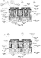
- FIGS. 1-2 illustrate stylized cross-sectional depictions of prior art vFET devices.
- FIG. 1 illustrates a vFET device 100 comprising a bottom S/D region 150 and a top S/D region 155 , separated by fins 130 and gate material 140 .
- the bottom S/D region 150 is formed on a substrate 110 .
- the vFET device 100 also comprises a bottom spacer 120 and a top spacer 125 .
- FIG. 2 illustrates a problem repeatedly encountered in the art.
- prior art vFET device 200 is prepared by reactive ion etching (ME) of amorphous carbon deposited on a patterned workpiece.
- ME reactive ion etching
- the critical dimension of an RIE patterning overlay is narrower than the width of fins 230 A, 230 B, and 230 C, and the patterning shifted with respect to the fins 230 A, 230 B, and 230 C
- WFM work function metal
- Plasma exposure can damage WFM layer 265 , thereby leading to a threshold voltage (V T ) shift of a vFET comprising a fin 230 A, 230 B, or 230 C.
- V T threshold voltage
- a high-k dielectric layer 260 underlying the WFM layer 265 may be exposed to plasma during RIE and thereby damaged. Damage to high-k dielectric layer 260 will also impair the function of a vFET comprising fin 230 C.
- a first source/drain (S/D) region may be formed on a substrate.
- a plurality of fins is formed on the substrate (and the first S/D region, if present).
- a gate structure is formed on at least a first side and a second side of a lower portion of each fin.
- a spacer is formed on at least a first side and a second side of an upper portion of each fin. At least one layer is formed above the substrate and between the fins. An opening is formed in the at least one layer between the fins by an etching process. The spacer protects the gate structure from the etching process.
- FIG. 1 illustrates a stylized cross-sectional depiction of a typical vFET device
- FIG. 2 illustrates a stylized cross-sectional view of a prior art vFET (device 300 ) under manufacture
- FIG. 3 illustrates a stylized plan depiction of a vFET device with X1-cut, X2-cut, and Z-cut lines of view indicated, in accordance with embodiments herein;
- FIG. 4 illustrates a stylized X1-cut cross-sectional depiction of the vFET device under manufacture with respect to fin, shallow trench isolation, first source/drain region, and bottom spacer formation processes, in accordance with embodiments herein;
- FIG. 5 illustrates a stylized X1-cut cross-sectional depiction of the vFET device under manufacture with respect to high-k dielectric layer and work function metal (WFM) layer formation processes, in accordance with embodiments herein;
- WFM work function metal
- FIG. 6 illustrates a stylized X2-cut cross-sectional depiction of the vFET device under manufacture with respect to high-k dielectric layer and WFM layer formation processes, in accordance with embodiments herein;
- FIG. 7 illustrates a stylized X1-cut cross-sectional depiction of the vFET device under manufacture with respect to an opening formation process, in accordance with embodiments herein;
- FIG. 8 illustrates a stylized X1-cut cross-sectional depiction of the vFET device under manufacture with respect to a nitride deposition process, in accordance with embodiments herein;
- FIG. 9 illustrates a stylized X1-cut cross-sectional depiction of the vFET device under manufacture with respect to oxide deposition and chemical-mechanical polishing (CMP) processes, in accordance with embodiments herein;
- FIG. 10 illustrates a stylized X1-cut cross-sectional depiction of the vFET device under manufacture with respect to an oxide recess process, in accordance with embodiments herein;
- FIG. 11 illustrates a stylized X1-cut cross-sectional depiction of the vFET device under manufacture with respect to an oxide liner deposition process, in accordance with embodiments herein;
- FIG. 12 illustrates a stylized X1-cut cross-sectional depiction of the vFET device under manufacture with respect to a nitride spacer deposition process, in accordance with embodiments herein;
- FIG. 13 illustrates a stylized Z-cut cross-sectional depiction of the vFET device under manufacture with respect to the nitride spacer deposition process, in accordance with embodiments herein;
- FIG. 14 illustrates a stylized Z-cut cross-sectional depiction of the vFET device under manufacture with respect to a lithography patterning process, in accordance with embodiments herein;
- FIG. 15 illustrates a stylized X1-cut cross-sectional depiction of the vFET device under manufacture with respect to a nitride spacer removal process, in accordance with embodiments herein;
- FIG. 16 illustrates a stylized Z-cut cross-sectional depiction of the vFET device under manufacture with respect to the nitride spacer removal process, in accordance with an embodiments herein;
- FIG. 17 illustrates a stylized X1-cut cross-sectional depiction of the vFET device under manufacture with respect to an opening formation process, in accordance with embodiments herein;
- FIG. 18 illustrates a stylized Z-cut cross-sectional depiction of the vFET device under manufacture with respect to the oxide layer removal process, in accordance with embodiments herein;
- FIG. 19 illustrates a stylized X1-cut cross-sectional depiction of the vFET device under manufacture with respect to a nitride layer removal process, in accordance with embodiments herein;
- FIG. 20 illustrates a stylized Z-cut cross-sectional depiction of the vFET device under manufacture with respect to the nitride layer removal process, in accordance with embodiments herein;
- FIG. 21 illustrates a stylized X1-cut cross-sectional depiction of the vFET device under manufacture with respect to WFM layer and high-k dielectric layer removal processes, in accordance with embodiments herein;
- FIG. 22 illustrates a stylized Z-cut cross-sectional depiction of the vFET device under manufacture with respect to the WFM layer and high-k dielectric layer removal processes, in accordance with embodiments herein;
- FIG. 23 illustrates a stylized Z-cut cross-sectional depiction of the vFET device under manufacture with respect to a patterning removal processes, in accordance with embodiments herein;
- FIG. 24 illustrates a stylized X1-cut cross-sectional depiction of the vFET device under manufacture with respect to oxide deposition and CMP processes, in accordance with embodiments herein;
- FIG. 25 illustrates a stylized Z-cut cross-sectional depiction of the vFET device under manufacture with respect to the oxide deposition and CMP processes, in accordance with embodiments herein;
- FIG. 26 illustrates a stylized X1-cut cross-sectional depiction of the vFET device under manufacture with respect to formation of a second source/drain region, in accordance with embodiments herein;
- FIG. 27 illustrates a flowchart depiction of process steps of providing a vFET device, in accordance with embodiments herein;
- FIG. 28 illustrates a flowchart depiction of process steps of providing a vFET device, in accordance with embodiments herein;
- FIG. 29 illustrates a stylized depiction of a system for fabricating a semiconductor device package comprising a vFET device, in accordance with embodiments herein.
- Embodiments herein provide for forming FET devices (e.g., vFET devices) with reduced damage to a WFM layer of the vFET devices.
- a vFET that comprises a plurality of fins comprising a work function metal (WFM) up to a first height on the sides of the fins and a nitride spacer at a second, greater height on the sides of the fins; a bottom source/drain (S/D) region below the fins; and a second S/D region above the fins.
- WFM work function metal
- S/D source/drain
- the described structure owing at least in part to the relation between the fin width at the first and second heights, provides a method to pattern vFET in a self-aligned way with reduced damage to a WFM layer during a pattering process.
- FIG. 3 illustrates a stylized plan depiction of a vFET device in accordance with embodiments herein.
- a connecting layer 340 is disposed over the first end 331 of a first plurality of fins 330 and over the second end 336 of a second plurality of fins 335 .
- the first end 331 and the second end 336 are proximate each other but are not in direct contact with each other.
- the first plurality of fins 330 are PFET components and the second plurality of fins 335 are NFET components.
- the first plurality of fins 330 are NFET components and the second plurality of fins 335 are PFET components.
- FIGS. 4-25 illustrate stylized cross-sectional depictions of a vFET device under various stage of manufacture, in accordance with embodiments herein.
- FIG. 4 illustrates a stylized X1-cut cross-sectional view of a vFET (device 300 ) under manufacture, in accordance with embodiments herein.
- initial FET processing steps known to those skilled in the art having benefit of the present disclosure may be performed to provide a FET device 300 under manufacture that comprises a first plurality of fins 330 comprising fins 330 A, 330 B, 330 C, 330 D.
- the device 300 comprises a substrate 310 (e.g., silicon substrate, silicon germanium substrate, etc.).
- a plurality of fins 330 A, 330 B, 330 C, 330 D are formed on the substrate 310 .
- the fins 330 A, 330 B, 330 C, and 330 D each comprise a fin body 332 .
- hardmask 345 of the first plurality of fins 330 may remain on top of the first plurality of fins 330 after the formation thereof.
- various features are formed on and/or in the substrate 310 , such as a bottom or first S/D region 350 , one or more STI regions 480 , and/or a bottom spacer 320 , among others which will be apparent to a person of ordinary skill in the art having the benefit of the present disclosure.
- Techniques for forming the various features depicted in FIG. 4 will be known to a person of ordinary skill in the art having benefit of the present disclosure, and need not be described further.
- FIG. 5 a stylized X1-cut cross-sectional depiction of the vFET device under manufacture with respect to high-k dielectric layer and WFM layer formation processes on the first plurality of fins 330 is illustrated, in accordance with embodiments herein.
- a high-k dielectric layer formation process is performed. This process comprises forming a high-k dielectric layer 560 over the first plurality of fins 330 and bottom spacer 320 .
- a person of ordinary skill in the art may form the high-k dielectric layer 560 as a routine matter.
- a WFM layer formation process is performed. This process comprises forming a WFM layer 565 over the high-k dielectric layer 560 .
- a person of ordinary skill in the art may form the WFM layer 565 as a routine matter, bearing in mind whether the first plurality of fins 330 will be components of a PFET or an NFET will be a significant factor in determining which work function metal may be selected for WFM layer 565 .
- the high-k dielectric layer 560 and the WFM layer 565 deposited above the first plurality of fins 330 are thin enough to leave spaces between fins, as shown in FIG. 5 .
- FIG. 6 illustrates a stylized X2-cut cross-sectional depiction of the vFET device under manufacture with respect to high-k dielectric layer and WFM layer formation processes on the second plurality of fins 335 , in accordance with embodiments herein.
- the high-k dielectric layer 560 may be formed as described above with reference to FIG. 5 .
- the WFM layer 667 may be formed as described above with reference to FIG. 5 , bearing in mind whether the second plurality of fins 335 will be components of a PFET or an NFET will be a significant factor in determining which work function metal may be selected for WFM layer 667 .
- WFM layer 565 and WFM layer 667 comprise different work function metals.
- first plurality of fins 330 and the second plurality of fins 335 will undergo generally identical processes. In the interest of brevity, only the first plurality of fins 330 of the vFET device under manufacture will be depicted. Processes performed on WFM layer 565 will be understood to also be performed on WFM layer 667 .
- FIG. 7 illustrates a stylized X1-cut cross-sectional depiction of the vFET device under manufacture with respect to an opening formation process, in accordance with embodiments herein.
- the high-k dielectric layer 560 and the WFM layer 565 are removed from the tops of the first plurality of fins 330 and from portions of the sides of the first plurality of fins 330 above a first height. Removal of the high-k dielectric layer 560 and the WFM layer 565 above the first height may be performed by any appropriate technique.
- removal of the high-k dielectric layer 560 and the WFM layer 565 above the first height may comprise depositing a sacrificial layer over the plurality of fins, performing CMP, and etching the sacrificial layer using process parameters which will also remove the portions of the high-k dielectric layer 560 and the WFM layer 565 above the first height.
- FIG. 8 illustrates a stylized X1-cut cross-sectional depiction of the vFET device under manufacture with respect to a nitride deposition process, in accordance with embodiments herein.
- a nitride layer 870 may be deposited over the first plurality of fins 330 using any appropriate technique.
- the nitride layer 870 may comprise silicon nitride.
- each fin structure 330 A-D that each comprises a fin body 332 , an hardmask 345 on the top, and a high-k dielectric layer 560 , a WFM layer 565 , and a nitride layer 870 on the sidewalls of each fin structure 330 A-D.
- Each fin e.g., fin 330 A, has a first width at the first height. The first width encompasses the width of the fin body 332 plus the width of the high-k dielectric layer 560 , the WFM layer 565 , and the nitride layer 870 on each side of the fin.
- FIG. 9 illustrates a stylized X1-cut cross-sectional depiction of the vFET device under manufacture with respect to oxide deposition and CMP processes, in accordance with embodiments herein.
- An oxide layer 972 may be deposited over the first plurality of fins 330 using any appropriate technique.
- the oxide layer 972 comprises silicon oxide.
- the oxide layer 972 may be deposited to a level over the tops of the fins 330 (not shown), and subsequently undergo a CMP process in order to lower the top of the oxide layer 972 to be substantially co-planar with the tops of the first plurality of fins 330 .
- FIG. 10 illustrates a stylized X1-cut cross-sectional depiction of the vFET device under manufacture with respect to an oxide recess process, in accordance with embodiments herein.
- An oxide layer 972 may be recessed using any appropriate technique. The oxide layer 972 may be recessed such that the top of the oxide layer 972 is below the tops of the first plurality of fins 330 and yet above the first height.
- FIG. 11 illustrates a stylized X1-cut cross-sectional depiction of the vFET device under manufacture with respect to an oxide liner deposition process, in accordance with embodiments herein.
- An oxide liner 1174 may be deposited over portions of nitride layer 870 that are exposed above the top of oxide layer 972 . (Any portion of the oxide liner 1174 deposited on oxide layer 972 will be hereinafter considered as being part of oxide layer 972 and will not be considered separately).
- the oxide liner 1174 may comprise silicon oxide. Though not to be bound by theory, the oxide liner 1174 may protect underlying portions of nitride layer 870 in subsequent operations.
- FIG. 12 illustrates a stylized X1-cut cross-sectional depiction of the vFET device under manufacture with respect to a nitride spacer deposition process, in accordance with embodiments herein.
- a nitride spacer 1286 is deposited over each member of the first plurality of fins 330 , and over oxide layer 972 between the fins 330 .
- the nitride spacer 1286 may be deposited by any appropriate technique.
- the nitride spacer 1286 may comprise silicon nitride.
- the nitride spacer 1286 is deposited to a thickness such that at a second height on the fins 330 , the second height is the height of the nitride spacer 1286 disposed between fins 330 , each fin 330 (e.g., fin 330 A), and has a second width, which is greater than the first width.
- the second width encompasses the thickness of fin body 332 and/or one or more of hardmask 345 , nitride layer 870 , oxide liner 1174 , and/or nitride spacer 1286 disposed on top of fin body 332 , and nitride layer 870 , oxide liner 1174 , and nitride spacer 1286 disposed on sidewalls of the fin.
- the first width is the lateral distance from an outer vertical face 1271 a of nitride layer 870 on a first side of the fin 330 A to an outer vertical face 1271 b of nitride layer 870 on a second side of the fin 330 A at the first height; and the second width is the lateral distance from an outer vertical face 1287 a of nitride spacer 1286 on a first side of the fin 330 A to an outer vertical face 1287 b of the nitride spacer 1286 on a second side of the fin 330 A at the second height.
- the space between the nitride spacer 1286 disposed on the sidewalls of adjacent fins 330 may be considered an opening 1282 .
- the opening 1282 has a third width at the second height. The opening 1282 will be discussed in more detail below.
- a nitride spacer 1286 prior to forming a nitride spacer 1286 as shown in FIG. 12 , other pluralities of fins (not shown) for which nitride spacer formation may not be desired may be masked. A person of ordinary skill in the art may mask such other pluralities of fins using known techniques in the art.
- FIG. 13 illustrates a stylized Z-cut cross-sectional depiction of the vFET device under manufacture with respect to the nitride spacer deposition process, in accordance with embodiments herein.
- the nitride spacer 1286 is deposited over both the first plurality of fins 330 and the second plurality of fins 335 .
- the nitride spacer 1286 is also deposited over oxide layer 972 between fins.
- FIG. 14 illustrates a stylized Z-cut cross-sectional depiction of the vFET device under manufacture with respect to a lithography patterning process, in accordance with embodiments herein.
- a contact feature 1478 is patterned such that landing pads in electrical contact with both WFM layer 565 of the first plurality of fins 330 and the WFM layer 667 of the second plurality of fins 335 may be manufactured in later operations.
- Lithography patterning techniques for forming the contact features 1478 will be known to a person of ordinary skill in the art and need not be described further.
- FIG. 15 illustrates a stylized X1-cut cross-sectional depiction of the vFET device under manufacture with respect to a nitride spacer removal process, in accordance with embodiments herein.
- FIG. 16 illustrates a stylized Z-cut cross-sectional depiction of the vFET device under manufacture with respect to the nitride spacer removal process, in accordance with embodiments herein.
- the nitride spacer 1286 is partially removed, e.g., from over the oxide liner 1174 on top of the fins 330 and from over the oxide layer 972 between the fins 330 .
- the nitride spacer 1286 is retained on the sidewalls of the fins 330 at least at the second height (and higher and/or lower, as may be desired).
- the nitride spacer 1286 may be removed by any appropriate technique, e.g., by etching selective to the oxide liner 1174 and the oxide layer 972 .
- FIG. 17 illustrates a stylized X1-cut cross-sectional depiction of the vFET device under manufacture with respect to an opening formation process, in accordance with an alternative embodiment.
- the opening 1282 is extended by partially removing the oxide layer 972 .
- the oxide layer 972 is partially removed between the fins 330 using nitride spacer 1286 as a mask.
- the oxide layer 972 not covered by nitride spacer 1286 may be removed and the opening 1282 formed by any appropriate technique, such as RIE.
- the nitride spacer 1286 provides protection to WFM layers 565 and 667 and high-k dielectric 560 during formation of the opening 1282 .
- the WFM layer 565 on the first side and the second side of the fin 330 A is not exposed to the opening 1282 .
- the opening 1282 is extended downward through the oxide layer 972 with minimal widening. Because the second width of each fin 330 , i.e., the width encompassing the nitride spacer 1286 at the second height, is greater than the first width of each fin 330 , i.e., the width encompassing the WFM layer 565 , downward extension with minimal widening of the opening 1282 reduces the likelihood of exposure of the WFM layer 565 to plasma used in the RIE process forming the opening 1282 . Accordingly, a vFET comprising the WFM layer 565 has a reduced threshold voltage shift. In other words, the opening 1282 is formed in a self-aligned process. FIG.
- FIG. 18 illustrates a stylized Z-cut cross-sectional depiction of the vFET device under manufacture with respect to the opening formation process, in accordance with embodiments herein.
- FIG. 18 shows the removal of the oxide liner 1174 above the fins 335 C.
- FIG. 19 illustrates a stylized X1-cut cross-sectional depiction of the vFET device under manufacture with respect to a nitride layer removal process, in accordance with embodiments herein.
- FIG. 20 illustrates a stylized Z-cut cross-sectional depiction of the vFET device under manufacture with respect to the nitride layer removal process, in accordance with embodiments herein.
- the exposed portion of nitride layer 870 at the bottom of the opening 1282 is removed.
- the portion of nitride layer 870 may be removed by any appropriate technique.
- Other portions of nitride layer 870 disposed directly under oxide layer 972 are retained.
- FIG. 21 illustrates a stylized X1-cut cross-sectional depiction of the vFET device under manufacture with respect to WFM layer and high-k dielectric layer removal processes, in accordance with embodiments herein.
- FIG. 22 illustrates a stylized Z-cut cross-sectional depiction of the vFET device under manufacture with respect to the WFM layer and high-k dielectric layer removal processes, in accordance with embodiments herein.
- the WFM layer 565 and the high-k dielectric layer 560 are partially removed at the bottom of the opening 1282 .
- the WFM layer 565 and the high-k dielectric layer 560 may be removed by any appropriate technique.
- a nitride liner (not shown) may be formed on a cross-sectional surface of the high-k dielectric layer 560 and the WFM layer 565 exposed to the opening 1282 , i.e., the sides of the high-k dielectric layer 560 and the WFM layer 565 where these layers are disposed on bottom spacer 320 between fins 330 A, 330 B.
- a nitride liner may protect the high-k dielectric layer 560 and/or the WFM layer 565 from being damaged during further operations.
- FIG. 23 illustrates a stylized Z-cut cross-sectional depiction of the vFET device under manufacture with respect to a patterning removal processes, in accordance with embodiments herein.
- the contact feature ( FIG. 22 , reference numeral 1478 ) may be removed by any appropriate technique.
- FIG. 24 illustrates a stylized X1-cut
- FIG. 25 a stylized Z-cut, cross-sectional depiction of the vFET device under manufacture with respect to oxide deposition and CMP processes, in accordance with embodiments herein.
- a second oxide layer 2573 may be deposited in openings 1282 , in areas between and/or around groups of fins (e.g., between fins 330 B and 330 C, to the left of fin 330 A, and to the right of fin 330 D), and in the area where the contact feature ( FIG. 22 , reference numeral 1478 ) was removed.
- a CMP process may be performed to make tops of the second oxide layer 2573 coplanar with the tops of fins 330 A-D. Being a dielectric material, the second oxide layer 2573 electrically isolates the WFM layers 565 of adjacent fins 330 .
- the second oxide layer 2573 may be deposited and CMP may be performed according to any appropriate technique.
- Further processes known to those skilled in the art may be performed to complete the processing of the vFET device.
- further processing steps e.g., source/drain (S/D) formation, silicide process, back-end-of-line (BEOL) may be performed to form MOSFET devices using FET processes.
- S/D source/drain
- BEOL back-end-of-line
- contacts may be formed through oxide layer 972 and/or second oxide layer 2573 to make electrical connections to the first S/D region 350 and/or the WFM layer 565 from features disposed above fins 330 , while maintaining electrical isolation of the WFM layers 565 of adjacent fins 330 .
- the nitride spacer 1286 , the oxide liner 1174 , and an upper portion of the nitride layer 870 may be removed from the fin structures 330 , and a second S/D region 2651 may be formed, such as by epitaxial growth of an appropriate S/D material.
- the drain and source regions for an NMOS device may be formed from n-doped silicon or low germanium percentage SiGe material.
- the drain and source regions for a PMOS device may be formed from p-doped germanium or high germanium percentage SiGe material. Accordingly, the processes exemplified herein may be used to provide N-FET and/or P-FET devices using the same base semiconductor structure.
- the process exemplified herein may be used to manufacture a vFET device comprising a first source/drain (S/D) region formed on a substrate; a plurality of fin structures formed above the first S/D region, wherein each the fin structure comprises a high-k dielectric layer and a work function metal (WFM) layer on at least a first side and a second side up to a first height, wherein the fin structure has a first width at the first height; and wherein each the fin structure comprises a nitride spacer on at least said first side and said second side at and above a second height, wherein the second height is greater than the first height, and each the fin structure has a second width at the second height, wherein the second width is greater than the first width; a gate region above the first S/D region and adjacent at least a portion of the fin structures; and a second S/D region above the plurality of fin structures.
- S/D source/drain
- WFM work function metal
- the vFET device may further comprise a contact between a first end of the plurality of fin structures and a second end of a second plurality of fin structures.
- the vFET device may further comprise a shallow trench isolation (STI) between two adjacent fin structures of the plurality of fin structures.
- the vFET device may further comprise a bottom spacer layer disposed on the first S/D region between the fin structures.
- the process 2700 may comprise forming a first source/drain (S/D) region on a substrate (at 2710 ), The process may further comprise forming (at 2715 ) a first plurality of fin structures above the first S/D) region, comprising forming a high-k dielectric layer up to a first height on at least at least a first side and a second side of each fin structure of the first plurality of fin structures, and forming a work function metal (WFM) layer on the high-k dielectric layer.
- WFM work function metal
- forming (at 2715 ) may comprise forming (at 2716 ) the high-k dielectric layer over the entirety of the first side and the second side and over a top of each fin structure; forming (at 2717 ) the WFM layer over the entirety of the high-k dielectric layer; and removing (at 2718 ) an upper portion of the high-k dielectric layer and an upper portion of the WFM layer from the top of each the fin structure and from the first side and the second side of each the fin structure down to the first height.
- the process may also comprise forming (at 2720 ) a nitride layer over the first plurality of fin structures, wherein each the fin structure has a first width at the first height.
- the nitride liner may comprise silicon nitride.
- the process may additionally comprise forming (at 2725 ) an oxide layer over the nitride layer, wherein a top of the oxide layer between the fin structures is above the first height.
- the forming (at 2725 ) may comprise depositing (at 2726 ) silicon oxide at least to a top of each the fin structure, polishing (at 2727 ) the silicon oxide to the top of each the fin structure, and recessing (at 2728 ) the silicon oxide between the fin structures to above the first height.
- the process may yet further comprise forming (at 2730 ) an oxide liner over the nitride layer.
- the process may yet additionally comprise forming (at 2732 ) a mask over pluralities of fins on which subsequent process steps are not desired to be performed.
- the process may comprise forming (at 2735 ) a nitride spacer over the oxide liner, wherein a top of the nitride spacer between the fin structures is at a second height, wherein the second height is greater than the first height; wherein each the fin structure has a second width at the second height, wherein the second width is greater than the first width; and wherein an opening between adjacent fins has a third width at the second height.
- the nitride spacer may comprise silicon nitride.
- the process may additionally comprise removing (at 2740 ) the nitride spacer, the oxide layer, the nitride layer, the WFM layer, and the high-k dielectric layer between the fin structures, whereby the opening between the adjacent fin structures has the third width at the first height and the third width at a base of each the fin structure.
- any of the actions of the process may further involve the formation and processing of a second plurality of fins, wherein the second plurality of fins ma be substantially the same as the first plurality.
- the first and second pluralities of fins may be disposed such that a first end of the first plurality is disposed in proximity to a second end of the second plurality.
- the process may further comprise one or more of the following.
- the process may further comprise patterning (at 2745 ) at least one contact the first end of the first plurality of fin structures and the second end of the second plurality of fin structures.
- the process may further comprise forming (at 2750 ) a nitride liner on portions of the high-k dielectric and the WFM layer exposed to the opening.
- the process may further comprise forming (at 2755 ) an oxide fill in the opening.
- the process may comprise completing (at 2760 ) device processing, e.g., forming a second S/D region above the plurality of fin structures, among other operations that will be known to a person of ordinary skill in the art.
- FIG. 28 depicts a flowchart of a process 2800 of providing a vFET device in accordance with embodiments herein.
- the process may comprise forming (at 2810 ) a first source/drain (S/D) region on a substrate.
- the process comprises forming (at 2815 ) a plurality of vertical fins on the substrate (and above the first S/D region, if present).
- the process further comprises forming (at 2820 ) a gate structure on at least a first side and a second side of a lower portion of each vertical fin.
- the process additionally comprises forming (at 2825 ) a spacer on at least a first side and a second side of an upper portion of each vertical fin.
- the process comprises forming (at 2830 ) at least one layer above the substrate and between the vertical fins.
- the process yet further comprises forming (at 2835 ) an opening in the at least one layer between the vertical fins by an etching process, wherein the spacer protects the gate structure during the etching process.
- the forming an opening (at 2835 ) may comprise performing (at 2836 ) a reactive ion etch (RIE).
- RIE reactive ion etch
- the process 2800 depicted in FIG. 28 may further comprise one or more of filling (at 2840 ) the opening with an oxide; removing (at 2845 ) the spacer from the vertical fins; forming (at 2850 ) a second source/drain (S/D) region above the plurality of vertical fins; and completing (at 2860 ) device processing.
- a system 2900 of FIG. 29 may comprise a semiconductor device processing system 2910 and a design unit 2940 .
- the semiconductor device processing system 2910 may manufacture integrated circuit devices based upon one or more designs provided by the design unit 2940 .
- the system 2900 is capable of performing at least one of the process steps described in FIGS. 4-26 .
- the processing system 2910 is capable of implementing the process described in the flowchart of FIG. 27 and/or FIG. 28 .
- the semiconductor device processing system 2910 may comprise various processing stations, such as etch process stations, photolithography process stations, CMP process stations, etc. Each of the processing stations may comprise one or more processing tools 2914 and or metrology tools 2916 . Feedback based on data from the metrology tools 2916 may be used to modify one or more process parameters used by the processing tools 2914 for performing process steps.
- the system 2910 may also comprise an interface 2912 that is capable of providing communications between the processing tools 2914 , the metrology tools 2916 and a controller, such as the processing controller 2920 .
- a controller such as the processing controller 2920 .
- One or more of the processing steps performed by the processing system 2910 may be controlled by the processing controller 2920 .
- the processing controller 2920 may be a workstation computer, a desktop computer, a laptop computer, a tablet computer, or any other type of computing device comprising one or more software products that are capable of controlling processes, receiving process feedback, receiving test results data, performing learning cycle adjustments, performing process adjustments, etc.
- the semiconductor device processing system 2910 may produce integrated circuits (e.g., vFET devices) on a medium, such as silicon wafers. More particularly, the semiconductor device processing system 2910 may produce integrated circuits having vFET devices wherein the fins have a first width at a first height and a second width at a second height, wherein the second width is greater than the first width.
- vFET devices integrated circuits
- the semiconductor device processing system 2910 may produce integrated circuits having vFET devices wherein the fins have a first width at a first height and a second width at a second height, wherein the second width is greater than the first width.
- the production of integrated circuits by the device processing system 2910 may be based upon the circuit designs provided by the integrated circuits design unit 2940 .
- the processing system 2910 may provide processed integrated circuits/devices 2915 on a transport mechanism 2950 , such as a conveyor system.
- the conveyor system may be sophisticated clean room transport systems that are capable of transporting semiconductor wafers.
- the semiconductor device processing system 2910 may comprise a plurality of processing steps, e.g., the 1 st process step, the 2 nd process step, etc., as described above.
- the items labeled “2915” may represent individual wafers, and in other embodiments, the items 2915 may represent a group of semiconductor wafers, e.g., a “lot” of semiconductor wafers.
- the integrated circuit or device 2915 may be a transistor, a capacitor, a resistor, a memory cell, a processor, and/or the like.
- the device 2915 is a transistor and the dielectric layer is a gate insulation layer for the transistor.
- the integrated circuit design unit 2940 of the system 2900 is capable of providing a circuit design that may be manufactured by the semiconductor processing system 2910 . This may include information regarding the first height, second height, first width, and second width for vFET devices described above.
- the integrated circuit design unit 2940 may be capable of determining the number of devices (e.g., processors, memory devices, etc.) to place in a device package.
- the integrated circuit design unit 2940 may also determine the height of the fins, the dimensions of the S/D regions, the dimensions of the bottom spacer, etc. These dimensions may be based upon data relating to drive currents/performance metrics, device dimensions, etc. Based upon such details of the devices, the integrated circuit design unit 2940 may determine specifications of the vFETs that are to be manufactured.
- the integrated circuit design unit 2940 may provide data for manufacturing a semiconductor device package described herein.
- the process steps set forth above are generally described in the context of vFETs, those skilled in the art would appreciate that the process steps may also be performed on standard FET devices.
- the system 2900 may be capable of performing analysis and manufacturing of various products involving various technologies.
- the system 2900 may receive design and production data for manufacturing devices of CMOS technology, Flash technology, BiCMOS technology, power devices, memory devices (e.g., DRAM devices), NAND memory devices, and/or various other semiconductor technologies. This data may be used by the system 2900 to fabricate the devices 300 described herein.
Abstract
Description
Claims (13)
Priority Applications (2)
| Application Number | Priority Date | Filing Date | Title |
|---|---|---|---|
| US15/676,005 US11309220B2 (en) | 2017-08-14 | 2017-08-14 | Methods, apparatus, and manufacturing system for self-aligned patterning of a vertical transistor |
| US17/722,653 US20220238386A1 (en) | 2017-08-14 | 2022-04-18 | Methods, apparatus, and manufacturing system for self-aligned patterning of a vertical transistor |
Applications Claiming Priority (1)
| Application Number | Priority Date | Filing Date | Title |
|---|---|---|---|
| US15/676,005 US11309220B2 (en) | 2017-08-14 | 2017-08-14 | Methods, apparatus, and manufacturing system for self-aligned patterning of a vertical transistor |
Related Child Applications (1)
| Application Number | Title | Priority Date | Filing Date |
|---|---|---|---|
| US17/722,653 Division US20220238386A1 (en) | 2017-08-14 | 2022-04-18 | Methods, apparatus, and manufacturing system for self-aligned patterning of a vertical transistor |
Publications (2)
| Publication Number | Publication Date |
|---|---|
| US20190051563A1 US20190051563A1 (en) | 2019-02-14 |
| US11309220B2 true US11309220B2 (en) | 2022-04-19 |
Family
ID=65274199
Family Applications (2)
| Application Number | Title | Priority Date | Filing Date |
|---|---|---|---|
| US15/676,005 Active US11309220B2 (en) | 2017-08-14 | 2017-08-14 | Methods, apparatus, and manufacturing system for self-aligned patterning of a vertical transistor |
| US17/722,653 Pending US20220238386A1 (en) | 2017-08-14 | 2022-04-18 | Methods, apparatus, and manufacturing system for self-aligned patterning of a vertical transistor |
Family Applications After (1)
| Application Number | Title | Priority Date | Filing Date |
|---|---|---|---|
| US17/722,653 Pending US20220238386A1 (en) | 2017-08-14 | 2022-04-18 | Methods, apparatus, and manufacturing system for self-aligned patterning of a vertical transistor |
Country Status (1)
| Country | Link |
|---|---|
| US (2) | US11309220B2 (en) |
Families Citing this family (7)
| Publication number | Priority date | Publication date | Assignee | Title |
|---|---|---|---|---|
| US11538939B2 (en) | 2020-01-14 | 2022-12-27 | International Business Machines Corporation | Controlled bottom junctions |
| US11177367B2 (en) | 2020-01-15 | 2021-11-16 | International Business Machines Corporation | Self-aligned bottom spacer EPI last flow for VTFET |
| US11251287B2 (en) | 2020-04-14 | 2022-02-15 | International Business Machines Corporation | Self-aligned uniform bottom spacers for VTFETS |
| CN113690137B (en) * | 2020-05-18 | 2023-05-26 | 中芯国际集成电路制造(上海)有限公司 | Method for forming semiconductor structure |
| US11621326B2 (en) * | 2020-12-17 | 2023-04-04 | International Business Machines Corporation | Vertical field effect transistor with crosslink fin arrangement |
| US20230072305A1 (en) * | 2021-09-09 | 2023-03-09 | International Business Machines Corporation | Vertical Transistor with Late Source/Drain Epitaxy |
| US11949011B2 (en) | 2021-11-30 | 2024-04-02 | International Business Machines Corporation | Vertical transistor with gate encapsulation layers |
Citations (12)
| Publication number | Priority date | Publication date | Assignee | Title |
|---|---|---|---|---|
| US20120104547A1 (en) * | 2010-11-01 | 2012-05-03 | International Business Machines Corporation | Lateral epitaxial grown soi in deep trench structures and methods of manufacture |
| US20130181263A1 (en) * | 2012-01-16 | 2013-07-18 | Globalfoundries Inc. | Methods of Forming a Dielectric Cap Layer on a Metal Gate Structure |
| US9412822B2 (en) * | 2014-03-07 | 2016-08-09 | Globalfoundries Inc. | Methods of forming stressed channel regions for a FinFET semiconductor device and the resulting device |
| US9478634B2 (en) * | 2014-11-07 | 2016-10-25 | Globalfoundries Inc. | Methods of forming replacement gate structures on finFET devices and the resulting devices |
| US20170179123A1 (en) * | 2015-05-15 | 2017-06-22 | Taiwan Semiconductor Manfactuning Company, Ltd. | Fin Field Effect Transistor (FinFET) Device Structure with Uneven Gate Structure |
| US9711618B1 (en) * | 2016-03-31 | 2017-07-18 | International Business Machines Corporation | Fabrication of vertical field effect transistor structure with controlled gate length |
| US9761491B1 (en) * | 2016-12-06 | 2017-09-12 | Globalfoundries Inc. | Self-aligned deep contact for vertical FET |
| US20170373167A1 (en) * | 2016-06-28 | 2017-12-28 | International Business Machines Corporation | Vertical transport field effect transistor with precise gate length definition |
| US20170373162A1 (en) * | 2016-06-24 | 2017-12-28 | International Business Machines Corporation | Fabrication of a vertical fin field effect transistor with a reduced contact resistance |
| US9870952B1 (en) * | 2017-02-07 | 2018-01-16 | International Business Machines Corporation | Formation of VFET and finFET |
| US9960271B1 (en) * | 2017-04-18 | 2018-05-01 | Globalfoundries Inc. | Method of forming vertical field effect transistors with different threshold voltages and the resulting integrated circuit structure |
| US20180240873A1 (en) * | 2017-02-21 | 2018-08-23 | International Business Machines Corporation | Techniques for VFET Top Source/Drain Epitaxy |
-
2017
- 2017-08-14 US US15/676,005 patent/US11309220B2/en active Active
-
2022
- 2022-04-18 US US17/722,653 patent/US20220238386A1/en active Pending
Patent Citations (17)
| Publication number | Priority date | Publication date | Assignee | Title |
|---|---|---|---|---|
| US20120104547A1 (en) * | 2010-11-01 | 2012-05-03 | International Business Machines Corporation | Lateral epitaxial grown soi in deep trench structures and methods of manufacture |
| US8232163B2 (en) * | 2010-11-01 | 2012-07-31 | International Business Machines Corporation | Lateral epitaxial grown SOI in deep trench structures and methods of manufacture |
| US20120261797A1 (en) * | 2010-11-01 | 2012-10-18 | International Business Machines Corporation | Lateral epitaxial grown soi in deep trench structures and methods of manufacture |
| US20140084418A1 (en) * | 2010-11-01 | 2014-03-27 | International Business Machines Corporation | Lateral epitaxial grown soi in deep trench structures and methods of manufacture |
| US8692307B2 (en) * | 2010-11-01 | 2014-04-08 | International Business Machines Corporation | Lateral epitaxial grown SOI in deep trench structures and methods of manufacture |
| US8836003B2 (en) * | 2010-11-01 | 2014-09-16 | International Business Machines Corporation | Lateral epitaxial grown SOI in deep trench structures and methods of manufacture |
| US20130181263A1 (en) * | 2012-01-16 | 2013-07-18 | Globalfoundries Inc. | Methods of Forming a Dielectric Cap Layer on a Metal Gate Structure |
| US9412822B2 (en) * | 2014-03-07 | 2016-08-09 | Globalfoundries Inc. | Methods of forming stressed channel regions for a FinFET semiconductor device and the resulting device |
| US9478634B2 (en) * | 2014-11-07 | 2016-10-25 | Globalfoundries Inc. | Methods of forming replacement gate structures on finFET devices and the resulting devices |
| US20170179123A1 (en) * | 2015-05-15 | 2017-06-22 | Taiwan Semiconductor Manfactuning Company, Ltd. | Fin Field Effect Transistor (FinFET) Device Structure with Uneven Gate Structure |
| US9711618B1 (en) * | 2016-03-31 | 2017-07-18 | International Business Machines Corporation | Fabrication of vertical field effect transistor structure with controlled gate length |
| US20170373162A1 (en) * | 2016-06-24 | 2017-12-28 | International Business Machines Corporation | Fabrication of a vertical fin field effect transistor with a reduced contact resistance |
| US20170373167A1 (en) * | 2016-06-28 | 2017-12-28 | International Business Machines Corporation | Vertical transport field effect transistor with precise gate length definition |
| US9761491B1 (en) * | 2016-12-06 | 2017-09-12 | Globalfoundries Inc. | Self-aligned deep contact for vertical FET |
| US9870952B1 (en) * | 2017-02-07 | 2018-01-16 | International Business Machines Corporation | Formation of VFET and finFET |
| US20180240873A1 (en) * | 2017-02-21 | 2018-08-23 | International Business Machines Corporation | Techniques for VFET Top Source/Drain Epitaxy |
| US9960271B1 (en) * | 2017-04-18 | 2018-05-01 | Globalfoundries Inc. | Method of forming vertical field effect transistors with different threshold voltages and the resulting integrated circuit structure |
Also Published As
| Publication number | Publication date |
|---|---|
| US20220238386A1 (en) | 2022-07-28 |
| US20190051563A1 (en) | 2019-02-14 |
Similar Documents
| Publication | Publication Date | Title |
|---|---|---|
| US20220238386A1 (en) | Methods, apparatus, and manufacturing system for self-aligned patterning of a vertical transistor | |
| US10121702B1 (en) | Methods, apparatus and system for forming source/drain contacts using early trench silicide cut | |
| US10263122B1 (en) | Methods, apparatus, and manufacturing system for self-aligned patterning of contacts in a vertical field effect transistor | |
| US10461173B1 (en) | Methods, apparatus, and manufacturing system for forming source and drain regions in a vertical field effect transistor | |
| US10269654B1 (en) | Methods, apparatus and system for replacement contact for a finFET device | |
| US11069677B2 (en) | Semiconductor device comprising metal-insulator-metal (MIM) capacitor | |
| US10204904B2 (en) | Methods, apparatus and system for vertical finFET device with reduced parasitic capacitance | |
| US20190355615A1 (en) | Methods, apparatus, and system for a semiconductor device comprising gates with short heights | |
| US10998422B2 (en) | Methods, apparatus and system for a self-aligned gate cut on a semiconductor device | |
| US10522639B2 (en) | Methods, apparatus and system for stringer defect reduction in a trench cut region of a finFET device | |
| US9960086B2 (en) | Methods, apparatus and system for self-aligned retrograde well doping for finFET devices | |
| US10644156B2 (en) | Methods, apparatus, and system for reducing gate cut gouging and/or gate height loss in semiconductor devices | |
| US10825913B2 (en) | Methods, apparatus, and manufacturing system for FinFET devices with reduced parasitic capacitance | |
| US10854515B2 (en) | Methods, apparatus, and system for protecting cobalt formations from oxidation during semiconductor device formation | |
| US10937693B2 (en) | Methods, apparatus and system for a local interconnect feature over an active region in a finFET device | |
| US10236291B2 (en) | Methods, apparatus and system for STI recess control for highly scaled finFET devices | |
| US10014209B2 (en) | Methods, apparatus and system for local isolation formation for finFET devices | |
| US10062612B2 (en) | Method and system for constructing FINFET devices having a super steep retrograde well | |
| US20200052106A1 (en) | Methods, apparatus, and system to control gate height and cap thickness across multiple gates | |
| US10707303B1 (en) | Method, apparatus, and system for improving scaling of isolation structures for gate, source, and/or drain contacts | |
| US10685881B2 (en) | Methods, apparatus, and manufacturing system for self-aligned patterning of contacts in a semiconductor device | |
| US10707207B1 (en) | Method, apparatus, and system for improved gate connections on isolation structures in FinFET devices | |
| US10153211B1 (en) | Methods, apparatus, and system for fabricating finFET devices with increased breakdown voltage |
Legal Events
| Date | Code | Title | Description |
|---|---|---|---|
| AS | Assignment |
Owner name: GLOBALFOUNDRIES INC., CAYMAN ISLANDS Free format text: ASSIGNMENT OF ASSIGNORS INTEREST;ASSIGNORS:PARK, CHANRO;XIE, RUILONG;SUNG, MIN GYU;SIGNING DATES FROM 20170810 TO 20170814;REEL/FRAME:043283/0524 |
|
| STPP | Information on status: patent application and granting procedure in general |
Free format text: RESPONSE TO NON-FINAL OFFICE ACTION ENTERED AND FORWARDED TO EXAMINER |
|
| STPP | Information on status: patent application and granting procedure in general |
Free format text: FINAL REJECTION MAILED |
|
| STPP | Information on status: patent application and granting procedure in general |
Free format text: RESPONSE AFTER FINAL ACTION FORWARDED TO EXAMINER |
|
| STPP | Information on status: patent application and granting procedure in general |
Free format text: ADVISORY ACTION MAILED |
|
| STPP | Information on status: patent application and granting procedure in general |
Free format text: NON FINAL ACTION MAILED |
|
| STPP | Information on status: patent application and granting procedure in general |
Free format text: RESPONSE TO NON-FINAL OFFICE ACTION ENTERED AND FORWARDED TO EXAMINER |
|
| STPP | Information on status: patent application and granting procedure in general |
Free format text: NON FINAL ACTION MAILED |
|
| STCB | Information on status: application discontinuation |
Free format text: ABANDONED -- FAILURE TO RESPOND TO AN OFFICE ACTION |
|
| AS | Assignment |
Owner name: GLOBALFOUNDRIES U.S. INC., CALIFORNIA Free format text: ASSIGNMENT OF ASSIGNORS INTEREST;ASSIGNOR:GLOBALFOUNDRIES INC.;REEL/FRAME:054633/0001 Effective date: 20201022 |
|
| STCC | Information on status: application revival |
Free format text: WITHDRAWN ABANDONMENT, AWAITING EXAMINER ACTION |
|
| STPP | Information on status: patent application and granting procedure in general |
Free format text: NON FINAL ACTION MAILED |
|
| STPP | Information on status: patent application and granting procedure in general |
Free format text: RESPONSE TO NON-FINAL OFFICE ACTION ENTERED AND FORWARDED TO EXAMINER |
|
| STPP | Information on status: patent application and granting procedure in general |
Free format text: FINAL REJECTION MAILED |
|
| AS | Assignment |
Owner name: GLOBALFOUNDRIES U.S. INC., NEW YORK Free format text: RELEASE BY SECURED PARTY;ASSIGNOR:WILMINGTON TRUST, NATIONAL ASSOCIATION;REEL/FRAME:056987/0001 Effective date: 20201117 |
|
| FEPP | Fee payment procedure |
Free format text: PETITION RELATED TO MAINTENANCE FEES GRANTED (ORIGINAL EVENT CODE: PTGR); ENTITY STATUS OF PATENT OWNER: LARGE ENTITY |
|
| STPP | Information on status: patent application and granting procedure in general |
Free format text: ADVISORY ACTION MAILED |
|
| STPP | Information on status: patent application and granting procedure in general |
Free format text: DOCKETED NEW CASE - READY FOR EXAMINATION |
|
| STPP | Information on status: patent application and granting procedure in general |
Free format text: NON FINAL ACTION MAILED |
|
| STPP | Information on status: patent application and granting procedure in general |
Free format text: RESPONSE TO NON-FINAL OFFICE ACTION ENTERED AND FORWARDED TO EXAMINER |
|
| STPP | Information on status: patent application and granting procedure in general |
Free format text: NOTICE OF ALLOWANCE MAILED -- APPLICATION RECEIVED IN OFFICE OF PUBLICATIONS |
|
| STPP | Information on status: patent application and granting procedure in general |
Free format text: PUBLICATIONS -- ISSUE FEE PAYMENT VERIFIED |
|
| STCF | Information on status: patent grant |
Free format text: PATENTED CASE |