US11309053B2 - Semiconductor memory device and storage device - Google Patents
Semiconductor memory device and storage device Download PDFInfo
- Publication number
- US11309053B2 US11309053B2 US17/009,404 US202017009404A US11309053B2 US 11309053 B2 US11309053 B2 US 11309053B2 US 202017009404 A US202017009404 A US 202017009404A US 11309053 B2 US11309053 B2 US 11309053B2
- Authority
- US
- United States
- Prior art keywords
- semiconductor memory
- memory device
- command
- waiting time
- memory controller
- Prior art date
- Legal status (The legal status is an assumption and is not a legal conclusion. Google has not performed a legal analysis and makes no representation as to the accuracy of the status listed.)
- Active
Links
Images


Classifications
-
- G—PHYSICS
- G11—INFORMATION STORAGE
- G11C—STATIC STORES
- G11C29/00—Checking stores for correct operation ; Subsequent repair; Testing stores during standby or offline operation
- G11C29/04—Detection or location of defective memory elements, e.g. cell constructio details, timing of test signals
- G11C29/08—Functional testing, e.g. testing during refresh, power-on self testing [POST] or distributed testing
- G11C29/12—Built-in arrangements for testing, e.g. built-in self testing [BIST] or interconnection details
- G11C29/44—Indication or identification of errors, e.g. for repair
-
- G—PHYSICS
- G11—INFORMATION STORAGE
- G11C—STATIC STORES
- G11C29/00—Checking stores for correct operation ; Subsequent repair; Testing stores during standby or offline operation
- G11C29/02—Detection or location of defective auxiliary circuits, e.g. defective refresh counters
- G11C29/028—Detection or location of defective auxiliary circuits, e.g. defective refresh counters with adaption or trimming of parameters
-
- G—PHYSICS
- G11—INFORMATION STORAGE
- G11C—STATIC STORES
- G11C29/00—Checking stores for correct operation ; Subsequent repair; Testing stores during standby or offline operation
- G11C29/04—Detection or location of defective memory elements, e.g. cell constructio details, timing of test signals
- G11C29/08—Functional testing, e.g. testing during refresh, power-on self testing [POST] or distributed testing
- G11C29/12—Built-in arrangements for testing, e.g. built-in self testing [BIST] or interconnection details
- G11C29/12015—Built-in arrangements for testing, e.g. built-in self testing [BIST] or interconnection details comprising clock generation or timing circuitry
-
- G—PHYSICS
- G11—INFORMATION STORAGE
- G11C—STATIC STORES
- G11C29/00—Checking stores for correct operation ; Subsequent repair; Testing stores during standby or offline operation
- G11C29/04—Detection or location of defective memory elements, e.g. cell constructio details, timing of test signals
- G11C29/08—Functional testing, e.g. testing during refresh, power-on self testing [POST] or distributed testing
- G11C29/12—Built-in arrangements for testing, e.g. built-in self testing [BIST] or interconnection details
- G11C29/14—Implementation of control logic, e.g. test mode decoders
-
- G—PHYSICS
- G11—INFORMATION STORAGE
- G11C—STATIC STORES
- G11C29/00—Checking stores for correct operation ; Subsequent repair; Testing stores during standby or offline operation
- G11C29/04—Detection or location of defective memory elements, e.g. cell constructio details, timing of test signals
- G11C29/08—Functional testing, e.g. testing during refresh, power-on self testing [POST] or distributed testing
- G11C29/12—Built-in arrangements for testing, e.g. built-in self testing [BIST] or interconnection details
- G11C29/38—Response verification devices
- G11C29/42—Response verification devices using error correcting codes [ECC] or parity check
-
- G—PHYSICS
- G11—INFORMATION STORAGE
- G11C—STATIC STORES
- G11C29/00—Checking stores for correct operation ; Subsequent repair; Testing stores during standby or offline operation
- G11C29/04—Detection or location of defective memory elements, e.g. cell constructio details, timing of test signals
- G11C29/08—Functional testing, e.g. testing during refresh, power-on self testing [POST] or distributed testing
- G11C29/12—Built-in arrangements for testing, e.g. built-in self testing [BIST] or interconnection details
- G11C2029/4402—Internal storage of test result, quality data, chip identification, repair information
Definitions
- Embodiments described herein relate generally to a semiconductor memory device and a storage device.
- a semiconductor memory device that determines a correction value for a signal by performing training is known. It is expected that the operation of such semiconductor memory devices should be more efficient.
- FIG. 1 is a block diagram showing a constitution of a storage device according to a first embodiment.
- FIG. 2 is a block diagram showing a constitution of a semiconductor memory device according to the first embodiment.
- FIG. 3 is a view showing an example of correspondence between the semiconductor memory devices and addresses according to the first embodiment.
- FIG. 4 is a timing chart showing a timing of receiving a training command and reference data in the semiconductor memory device according to the first embodiment.
- FIG. 5 is a flowchart showing an operation of the semiconductor memory device according to the first embodiment.
- FIG. 6 is a block diagram showing a constitution of a storage device according to a second embodiment.
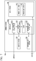
- FIG. 7 is a block diagram showing a constitution of a semiconductor memory device according to the second embodiment.
- FIG. 8 is a flowchart showing an operation of the semiconductor memory device according to the second embodiment.
- a semiconductor memory device of an embodiment includes a memory cell array, a processing circuit, a timer, a command decoder, and a training circuit.
- the memory cell array includes a plurality of memory cells.
- the processing circuit writes data into the memory cell array.
- the timer sets a waiting time.
- the command decoder receives a command output from a memory controller.
- the training circuit waits until the waiting time has passed since a predetermined command is received by the command decoder and performs a process relating to determination of a correction value for a signal sent from the memory controller to the processing circuit based on reference data output from the memory controller after the waiting time has passed.
- based on XX means “based at least on XX” and also includes a case based on another element in addition to XX. Further, “based on XX” is not limited to a case in which XX is used directly and also includes a case in which XX is based on a calculation or processing. “XX” is an arbitrary element (for example, arbitrary information). In this specification, “connection” also includes a case of electrical connection.
- FIG. 1 is a block diagram showing a constitution of a storage device 1 according to a first embodiment.
- the storage device 1 is to be connected to a host device in a communicative manner and to be used as a storage space for the host device.
- the storage device 1 is, for example, a storage device such as a solid state drive (SSD).
- SSD solid state drive
- the storage device 1 is mounted in, for example, a server device in a data center or an information processing device such as a personal computer (hereinafter, referred to as a “PC”).
- the storage device 1 is not limited thereto and may be, for example, a universal serial bus (USB) memory or an SD (registered trademark) memory card.
- USB universal serial bus
- SD registered trademark
- the host device is, for example, a server device in a data center or an information processing device such as a PC, but is not limited thereto.
- the host device broadly refers to a system to which the storage device 1 is connected in a communicative manner.
- the host device may be referred to as an “external device”.
- the “command” broadly means an instruction which causes a computer (for example, the storage device 1 ) to execute a target process.
- the “command” in this application is not limited to an instruction output by the host device, and includes an instruction generated inside the storage device 1 based on an instruction received from the host device, and an instruction regarding an internal process of the storage device 1 .
- the “command” may be read as “instruction”, “order”, “signal”, or the like.
- the “write command” is a command which includes information which indicates a write destination of communication data (for example, a write destination logical address).
- the host device outputs a read command to the storage device 1 , for example, when the communication data written in the storage device 1 is read.
- the “read command” is a command which includes information which indicates a read destination of communication data to be read by the host device (for example, a read destination logical address).
- the host device outputs an erase command to the storage device 1 , for example, when at least a part of the communication data written in the storage device 1 is to be erased.
- the “erase command” is a command which designates a region in which the communication data to be erased is written.
- the storage device 1 includes a plurality of (for example, three) semiconductor memory devices 10 , a memory controller 20 , a DRAM 30 , and a case (not shown) which accommodates these elements.
- the number of semiconductor memory devices 10 may be two, or more than three as long as the number is plural.
- Each of the plurality of semiconductor memory devices 10 and the memory controller 20 constitute a module mounted on the same board (not shown).
- the board is, for example, a printed circuit board.
- the plurality of semiconductor memory devices 10 , the memory controller 20 , and the DRAM 30 are mounted on this board.
- the semiconductor memory device 10 is an example of a semiconductor module.
- the plurality of semiconductor memory devices 10 are arranged and disposed on the board.
- the plurality of semiconductor memory devices 10 are electrically connected to the memory controller 20 in parallel with each other.
- the constitution and function of the semiconductor memory device 10 will be described later in detail.
- the semiconductor memory device 10 is, for example, a nonvolatile memory device, and is, for example, a NAND flash memory.
- the memory controller 20 is located between the host device and each of the plurality of semiconductor memory devices 10 .
- the memory controller 20 controls the plurality of semiconductor memory devices 10 as a whole.
- the DRAM (dynamic random access memory) 30 holds various management data. Further, the DRAM 30 serves as a cache memory. Other storage media may be used instead of the DRAM 30 .
- FIG. 2 is a block diagram showing the constitution of the semiconductor memory device 10 a according to the first embodiment.
- the semiconductor memory device 10 a includes a controller 100 a , an address storage 110 , a reference data storage 120 , a correction data storage 130 , and a data storage 140 .
- the controller 100 a includes a command decoder 101 a , an address recognition circuit 102 , a timer 103 , a detector 105 , and a corrector 106 .
- the detector 105 , the corrector 106 , the reference data storage 120 , and the correction data storage 130 constitute a training circuit TR.
- the controller 100 a controls various processes in the semiconductor memory device 10 a based on the command received from the memory controller 20 .
- the various processes referred to in this specification include writing of communication data to the data storage 140 , reading or erasing of communication data stored in the data storage 140 , communication training between the own semiconductor memory device 10 a and the memory controller 20 , or the like.
- the communication training is a timing adjustment of mutual processing between the semiconductor memory device 10 a and the memory controller 20 .
- the command decoder 101 a receives various commands output from the memory controller 20 .
- the various commands here are, for example, the above-described write command, read command, erase command, or the like.
- the various commands referred to here also include a “training command”.
- the training command is a command which indicates an instruction to execute the communication training between the semiconductor memory device 10 a and the memory controller 20 .
- the training command is output from the memory controller 20 to each of the semiconductor memory devices 10 at the time of, for example, starting up the storage device 1 , changing a setting, or the like.
- the command decoder 101 a When receiving the command, the command decoder 101 a identifies a type of the command. For example, the command decoder 101 a refers to information in which a command is associated with the type of the command (hereinafter, referred to as “correspondence information”). The correspondence information is stored in advance in, for example, a storage medium (not shown) included in the semiconductor memory device 10 a . The command decoder 101 a compares the received commands with the command included in the correspondence information, to identify the type of the received command.
- the controller 100 a performs various processes according to the type of the received command. For example, in a case where the command received by the command decoder 101 a is a write command, the controller 100 a write the communication data to the data storage 140 . Further, for example, in a case where the command received by the command decoder 101 a is a read command, the controller 100 a reads the communication data stored in the data storage 140 . Furthermore, for example, in a case where the command received by the command decoder 101 a is an erase command, the controller 100 a performs erasing of the communication data stored in the data storage 140 .
- the command decoder 101 a outputs a predetermined signal to the address recognition circuit 102 .
- the address recognition circuit 102 reads an address stored in the address storage 110 .
- the address storage 110 stores in advance information which indicates an address uniquely assigned to the own semiconductor memory device 10 a.
- FIG. 3 is a view showing an example of correspondence between the semiconductor memory devices 10 a and addresses according to the first embodiment.
- the address is a value which is unique to each of the semiconductor memory devices 10 a and is assigned in advance to be a continuous value.
- the address recognition circuit 102 determines a time to be set in the timer 103 based on the received address value and a length of a predetermined period. The address recognition circuit 102 sets the determined time in the timer 103 .
- the predetermined period corresponds to a length of time required for one communication training. For example, it is assumed that the time required for one communication training is 100 microseconds.
- the address recognition circuit 102 multiplies 0 by 100 and sets the calculation result (0 microsecond) to the timer 103 .
- the address recognition circuit 102 multiplies 1 by 100 and sets the calculation result (100 microseconds) to the timer 103 .
- the address recognition circuit 102 multiplies 2 by 100 and sets the calculation result (200 microseconds) to the timer 103 .
- the timer 103 outputs an enable signal to the training circuit TR (the detector 105 ) at a timing when the time set by the address recognition circuit 102 has passed.
- the training circuit TR starts execution of the communication training.
- the start of the execution of the communication training refers to the start of the communication training between the semiconductor memory device 10 a and the memory controller 20 .
- the communication training refers to performing a timing adjustment of the mutual processing between the semiconductor memory device 10 a and the memory controller 20 .
- the detector 105 receives the enable signal output from the timer 103 . When receiving the enable signal, the detector 105 receives the data output from the memory controller 20 .
- the constitution of the corrector 106 will be described later.
- the data received by the detector 105 is reference data.
- the reference data here is known data which is recognized in advance by both the semiconductor memory device 10 a and the memory controller 20 .
- the reference data storage 120 stores the reference data in advance.
- the detector 105 compares the reference data received from the memory controller 20 with the reference data stored in the reference data storage 120 , to generate correction data.
- the correction data is, for example, a difference value between the reference data received from the memory controller 20 and the reference data stored in the reference data storage 120 .
- the correction data is not limited to a difference value and may be, for example, a parameter of a calculation formula for correcting the difference value.
- the correction data may be data for correcting a phase of a signal which indicates the reference data, a waveform shape of the signal, or a duty ratio of the signal.
- the correction data storage 130 stores the correction data.
- the detector 105 stores the generated correction data in the correction data storage 130 .
- the memory controller 20 broadcasts a common training command to all the semiconductor memory devices 10 a and then sequentially outputs the reference data for each of the semiconductor memory devices 10 a at a predetermined timing (for example, following the above-described broadcast).
- the corrector 106 receives the communication data output from the memory controller 20 .
- the corrector 106 corrects the received communication data using the correction data stored in the correction data storage 130 .
- the corrector 106 writes the corrected communication data into the data storage 140 .
- the constitution of the corrector 106 described above is a constitution in the case in which the command decoder 101 a receives the write command, but the same applies to a case in which the read command is not received.
- the corrector 106 reads the communication data designated by the read command from the data storage 140 .
- the corrector 106 corrects the read communication data using the correction data stored in the correction data storage 130 .
- the corrector 106 outputs the corrected communication data to the memory controller 20 .
- the correction target is not limited to the communication data and may be, for example, a clock, a strobe, or the like.
- the data storage 140 is a storage medium which stores a variety of data.
- the data storage 140 includes a memory cell array 141 and a processing circuit 142 .
- the memory cell array 141 includes a plurality of memory cells.
- the processing circuit 142 performs data writing, reading, erasing, or the like on the memory cell array 141 .
- FIG. 4 is a timing chart showing a timing of receiving the training command and the reference data in the semiconductor memory device 10 a according to the first embodiment.
- the memory controller 20 outputs the common training command to all the semiconductor memory devices 10 a .
- the training command is broadcast to all the semiconductor memory devices 10 a .
- the semiconductor memory device 10 a - 1 , the semiconductor memory device 10 a - 2 , and the semiconductor memory device 10 a - 3 receive the training command output from the memory controller 20 .
- each of the semiconductor memory devices 10 a sets a time for the timer 103 . For example, 0 microsecond is set in the timer 103 of the semiconductor memory device 10 a - 1 , 100 microsecond is set in the timer 103 of the semiconductor memory device 10 a - 2 , and 200 microsecond is set in the timer 103 of the semiconductor memory device 10 a - 3 .
- the memory controller 20 After outputting the training command, the memory controller 20 next outputs the reference data for the semiconductor memory device 10 a - 1 (hereinafter, referred to as “reference data for 10 a - 1 ”).
- the reference data is broadcast to all the semiconductor memory devices 10 a .
- the semiconductor memory device 10 a - 1 , the semiconductor memory device 10 a - 2 , and the semiconductor memory device 10 a - 3 receive the reference data for 10 a - 1 output from the memory controller 20 .
- the timer is set so that the training circuit TR of the semiconductor memory device 10 a - 1 is validated at the timing when the semiconductor memory device 10 a - 1 receives the reference data for 10 a - 1 output from the memory controller 20 .
- the semiconductor memory device 10 a - 1 performs the communication training using the reference data for 10 a - 1 which is reference data for its own device. On the other hand, the semiconductor memory devices 10 a - 2 and the semiconductor memory device 10 a - 3 are in a waiting state since the time set in the timer 103 has not passed.
- the memory controller 20 After outputting the reference data for 10 a - 1 , the memory controller 20 outputs the reference data for the semiconductor memory device 10 a - 2 (hereinafter, referred to as “reference data for 10 a - 2 ”).
- the semiconductor memory devices 10 a - 1 , the semiconductor memory device 10 a - 2 , and the semiconductor memory device 10 a - 3 receive the reference data for 10 a - 2 output from the memory controller 20 .
- the timer is set so that the training circuit TR of the semiconductor memory device 10 a - 2 is validated at the timing when the semiconductor memory device 10 a - 2 receives the reference data for 10 a - 2 output from the memory controller 20 .
- the semiconductor memory device 10 a - 2 performs the communication training using the reference data for 10 a - 2 which is reference data for its own device. On the other hand, the semiconductor memory devices 10 a - 3 is still in the waiting state since the time set in the timer 103 has not passed.
- the memory controller 20 After outputting the reference data for 10 a - 2 , the memory controller 20 outputs the reference data for the semiconductor memory device 10 a - 3 (hereinafter, referred to as “reference data for 10 a - 3 ”).
- the semiconductor memory devices 10 a - 1 , the semiconductor memory device 10 a - 2 , and the semiconductor memory device 10 a - 3 receive the reference data for 10 a - 3 output from the memory controller 20 .
- the timer is set so that the training circuit TR of the semiconductor memory device 10 a - 3 is validated at the timing when the semiconductor memory device 10 a - 3 receives the reference data for 10 a - 3 output from the memory controller 20 .
- the semiconductor memory device 10 a - 3 performs the communication training using the reference data for 10 a - 3 which is reference data for its own device.
- the storage device 1 including the semiconductor memory device 10 a for example, in a case where the number of semiconductor memory devices 10 a is three, one training command output period and three reference data output periods are required to complete the communication training between all the semiconductor memory devices 10 a and the memory controller 20 . That is, for example, in a case where the number of the semiconductor memory devices 10 a is three, a total of four periods are required.
- a case in which, for example, the memory controller 20 sequentially outputs the training command and the reference data for each of the semiconductor memory devices 10 a is considered.
- the number of semiconductor memory devices 10 a is three
- three training command output period and three reference data output periods are required. That is, for example, in a case where the number of the semiconductor memory devices 10 a is three, a total of six periods are required.
- the storage device 1 including the semiconductor memory device 10 a according to the first embodiment as described above, the communication training between each of the semiconductor memory devices 10 a and the memory controller 20 can be completed in a total of four periods. In this way, the storage device 1 according to the first embodiment can reduce the time required for communication training.
- FIG. 5 is a flowchart showing the operation of the semiconductor memory device 10 a according to the first embodiment.
- the command decoder 101 a receives a command output from the memory controller 20 (Step S 001 ).
- the command decoder 101 a identifies the type of the received command.
- the controller 100 a performs various processes according to the type of the received command (Step S 003 ).
- the command decoder 101 a In a case where the received command is the training command (Yes in Step S 002 ), the command decoder 101 a outputs a predetermined signal to the address recognition circuit 102 .
- the address recognition circuit 102 When receiving the predetermined signal from the command decoder 101 a , the address recognition circuit 102 reads the address stored in the address storage 110 (Step S 004 ). The address recognition circuit 102 determines a time to be set in the timer 103 based on the received address value and a length of the predetermined period. The address recognition circuit 102 sets the determined time in the timer 103 (Step S 005 ).
- Step S 006 When the time set by the address recognition circuit 102 has not passed (No in Step S 006 ), the timer 103 is in the waiting state. When the time set by the address recognition circuit 102 has passed (Yes in Step S 006 ), the timer 103 outputs the enable signal to the training circuit TR (the detector 105 ) (Step S 007 ). When receiving the enable signal output from the timer 103 , the detector 105 validates its own training circuit TR (Step S 008 ).
- the detector 105 waits until receiving the reference data output from the memory controller 20 (No in Step S 009 ). When receiving the reference data (Yes in Step S 009 ), the detector 105 starts the execution of the communication training (Step S 010 ).
- the detector 105 compares the reference data received from the memory controller 20 with the reference data stored in the reference data storage 120 , to generate correction data (Step S 011 ).
- the detector 105 stores the generated correction data in the correction data storage 130 (Step S 012 ).
- the detector 105 invalidates its own training circuit TR (Step S 013 ).
- the operation of the semiconductor memory device 10 a shown in the flowchart of FIG. 5 is ended.
- the storage device 1 includes the memory controller 20 which broadcasts the training command to the plurality of semiconductor memory devices 10 a . Then, after broadcasting the training command, the memory controller 20 sequentially outputs the reference data to each of the semiconductor memory devices 10 a at different timings. Further, the storage device 1 has the plurality of semiconductor memory devices 10 a including the command decoder 101 a which receives a command output from the memory controller 20 . Furthermore, when the command decoder 101 a receives the training command, each of the semiconductor memory devices 10 a performs the communication training using the reference data received at a different timing for each of the semiconductor memory devices 10 a.
- each of the semiconductor memory devices 10 a sets the timer 103 so that the training circuit TR is validated at a timing when receiving the reference data for its own semiconductor memory device 10 a .
- the time set in the timer 103 is determined based on, for example, the address value uniquely assigned to be a continuous value in the plurality of semiconductor memory devices 10 a and a time required for communication training.
- the storage device 1 can start the communication training in all the semiconductor memory devices 10 a in order only by broadcasting the common training command only once from the memory controller to all the semiconductor memory devices 10 a . That is, the storage device 1 can reduce an output time of the training command to an output time of one training command. Thus, efficiency of the operation of the storage device 1 can be improved.
- the execution start timing of the communication training in the semiconductor memory device 10 a is controlled by the timer 103 provided in the semiconductor memory device 10 a .
- Such a constitution in which the communication timing is controlled by the timer 103 can be applied, for example, to a case in which the semiconductor memory device returns, for example, the communication data or the command to the memory controller at a predetermined timing according to a request from the memory controller.
- the memory controller (hereinafter, referred to as “memory controller 20 b ”) includes a training circuit TR which performs the communication training.
- the memory controller 20 b broadcasts a reference data request command to a plurality of semiconductor memory devices (hereinafter, referred to as “semiconductor memory devices 10 b ”) according to a second embodiment.
- the “reference data request command” is a command in which the memory controller 20 b requests each of the semiconductor memory devices 10 b to output the reference data to its own memory controller 20 b .
- the reference data request command is output from the memory controller 20 b to each of the semiconductor memory devices 10 b , for example, when the storage device 2 is activated or when the setting is changed.
- the reference data is stored in advance in each of the semiconductor memory devices 10 b.
- Each of the semiconductor memory devices 10 b outputs the reference data to the memory controller 20 b at a timing when a time set in the timer 103 has passed.
- the time set in the timer 103 is determined based on, for example, an address value which is uniquely assigned to be a continuous value in the plurality of semiconductor memory devices 10 b and a time required for outputting the reference data. Accordingly, the memory controller 20 b can sequentially receive the reference data output from the plurality of semiconductor memory devices 10 b at different timings.
- FIG. 6 is a block diagram showing a constitution of the storage device 2 according to the second embodiment.
- the storage device 2 includes a plurality of (for example, three) semiconductor memory devices 10 b , a memory controller 20 b , a DRAM 30 , and a case (not shown) which accommodates these elements.
- the memory controller 20 b includes a training circuit TR.
- the training circuit TR includes a reference data storage 220 , a detector 205 , a correction data storage 230 , and a corrector 206 .
- the constitutions of the reference data storage 220 , the detector 205 , the correction data storage 230 , and the corrector 206 respectively correspond to the constitutions of the reference data storage 120 , the detector 105 , the correction data storage 130 , and the corrector 106 of the storage device 1 according to the first embodiment.
- the memory controller 20 b broadcasts a reference data request command to the plurality of semiconductor memory devices 10 b . Then, the detector 205 of the memory controller 20 b sequentially receives the reference data output from each of the plurality of semiconductor memory devices 10 b at different timings.
- the detector 205 When receiving the reference data, the detector 205 starts execution of the communication training. The detector 205 compares the reference data received from the semiconductor memory device 10 b with reference data stored in the reference data storage 220 in advance, to generate correction data. The detector 205 stores the generated correction data in the correction data storage 230 .
- the corrector 206 corrects the received communication data using the correction data stored in the correction data storage 230 .
- the corrector 206 outputs the corrected communication data to the host device. Further, when receiving the communication data output from the host device, the corrector 206 corrects the received communication data using the correction data stored in the correction data storage 230 .
- the corrector 206 outputs the corrected communication data to the semiconductor memory device 10 b.
- FIG. 7 is a block diagram showing the constitution of the semiconductor memory device 10 b according to the second embodiment.
- the semiconductor memory device 10 b includes a controller 100 b , an address storage 110 , a reference data storage 120 , and a data storage 140 .
- the controller 100 b includes a command decoder 101 b , an address recognition circuit 102 , a timer 103 , and a reference data output unit 107 .
- the controller 100 b controls various processes in the semiconductor memory device 10 b based on the command received from the memory controller 20 .
- the various processes referred to this specification include, for example, writing of the communication data to the data storage 140 , reading or erasing of communication data stored in the data storage 140 , and outputting of the reference data to the memory controller 20 .
- the command decoder 101 b receives various commands output from the memory controller 20 .
- the various commands here are, for example, the above-described write command, read command, erase command, or the like.
- the various commands also include the above-described reference data request command.
- the command decoder 101 b When receiving the command, the command decoder 101 b identifies a type of the command. For example, the command decoder 101 b refers to correspondence information in which a command is associated with the type of the command. The correspondence information is stored in advance in, for example, a storage medium (not shown) included in the semiconductor memory device 10 b . The command decoder 101 b compares the received command with the command included in the correspondence information, to identify the type of the received command.
- the controller 100 b performs various processes according to the type of the received command.
- the command decoder 101 b outputs a predetermined signal to the address recognition circuit 102 .
- the address recognition circuit 102 reads the address stored in the address storage 110 .
- the address storage 110 stores in advance information which indicates an address uniquely assigned to its own semiconductor memory device 10 b .
- the address is a value which is unique to each of the semiconductor memory devices 10 b and is assigned in advance to be a continuous value.
- the address recognition circuit 102 determines a time to be set in the timer 103 based on the received address value and a length of a predetermined period. The address recognition circuit 102 sets the determined time in the timer 103 .
- the predetermined period corresponds to a length of time required for outputting the reference data to the memory controller 20 . It is assumed that the length of time required for outputting the reference data to the memory controller 20 is the same in each of the semiconductor memory devices 10 b . For example, it is assumed that the time required for outputting the reference data is 100 microseconds. Further, for example, the number of the semiconductor memory devices 10 b is three including a semiconductor memory device 10 b - 1 , a semiconductor memory device 10 b - 2 , and a semiconductor memory device 10 b - 3 . In this case, for example, “0”, “1”, and “2” are assigned in advance to the semiconductor memory devices 10 b - 1 , 10 b - 2 , and 10 b - 3 as addresses.
- the address recognition circuit 102 multiplies 0 by 100 and sets the calculation result (0 microsecond) to the timer 103 .
- the address recognition circuit 102 multiplies 1 by 100 and sets the calculation result (100 microseconds) to the timer 103 .
- the address recognition circuit 102 multiplies 2 by 100 and sets the calculation result (200 microseconds) to the timer 103 .
- the timer 103 outputs an enable signal to the reference data output unit 107 at a timing when the time set by the address recognition circuit 102 has passed.
- the reference data storage 120 stores the reference data in advance.
- the reference data output unit 107 receives the enable signal output from the timer 103 . When receiving the enable signal output from the timer 103 , the reference data output unit 107 reads the reference data stored in the reference data storage 120 . Additionally, the reference data output unit 107 outputs the read reference data to the memory controller 20 .
- the reference data output unit 107 is an example of a “data output unit”.
- the data storage 140 is a storage medium which stores a variety of data.
- the data storage 140 includes a memory cell array 141 and a processing circuit 142 .
- the memory cell array 141 includes a plurality of memory cells.
- the processing circuit 142 performs data writing, reading, erasing, or the like on the memory cell array 141 .
- the data storage 140 stores, for example, communication data.
- the communication data stored in the data storage 140 is read, for example, according to the read command output from the memory controller 20 . Then, the read communication data is corrected by the corrector 206 of the memory controller 20 b as described above. Further, the communication data stored in the data storage 140 is written according to, for example, the write command output from the memory controller 20 .
- the communication data written in this case is communication data which is output from the host device as described above and corrected by the corrector 206 of the memory controller 20 b.
- FIG. 8 is a flowchart showing the operation of the semiconductor memory device 10 b according to the second embodiment.
- the command decoder 101 b receives a command output from the memory controller 20 (Step S 101 ).
- the command decoder 101 b identifies the type of the received command. In a case where the received command is not the reference data request command (Step S 102 : No), the controller 100 b performs various processes according to the type of the received command (Step S 103 ).
- the command decoder 101 b In a case where the received command is the reference data request command (Yes in Step S 102 ), the command decoder 101 b outputs a predetermined signal to the address recognition circuit 102 .
- the address recognition circuit 102 When receiving the predetermined signal from the command decoder 101 b , the address recognition circuit 102 reads the address stored in the address storage 110 (Step S 104 ). The address recognition circuit 102 determines a time to be set in the timer 103 based on the received address value and a length of the predetermined period. The address recognition circuit 102 sets the determined time in the timer 103 (Step S 105 ).
- Step S 106 When the time set by the address recognition circuit 102 has not passed (No in Step S 106 ), the timer 103 is in the waiting state. When the time set by the address recognition circuit 102 has passed (Yes in Step S 106 ), the timer 103 outputs the enable signal to the reference data output unit 107 (Step S 107 ). When receiving the enable signal output from the timer 103 , the reference data output unit 107 reads the reference data stored in the reference data storage 120 (Step S 108 ).
- the reference data output unit 107 outputs the read reference data to the memory controller 20 (Step S 109 ).
- Step S 109 the operation of the semiconductor memory device 10 b shown in the flowchart of FIG. 8 is ended.
- each of the semiconductor memory devices 10 b includes the command decoder 101 b which receives the command output from the memory controller 20 . Furthermore, when the command decoder 101 b receives the reference data request command, each of the semiconductor memory devices 10 b outputs the reference data to the memory controller 20 at a different timing for each of the semiconductor memory devices 10 b.
- each of the semiconductor memory devices 10 b sets the timer 103 so that the output of the reference data is performed at a predetermined timing.
- the time set in the timer 103 is determined based on, for example, an address value uniquely assigned to be a continuous value in the plurality of semiconductor memory devices 10 b and a time required for outputting reference data.
- the storage device according to the second embodiment can collect the reference data from all the semiconductor memory devices 10 b in order only by broadcasting the common reference data request command only once from the memory controller 20 to all the semiconductor memory devices 10 b . That is, the storage device according to the second embodiment can reduce the output time of the reference data request command to the output time of one reference data request command. Thus, efficiency of the operation of the storage device according to the second embodiment can be improved.
- the storage device can improve the efficiency of the operation by including the command decoder 101 ( 101 a and 101 b ) which receives the command output from the memory controller 20 , and the function unit (the controller 100 a and the controller 100 b ) which performs the communication training between the memory controller 20 and its own device at a point in time when the predetermined time has passed since the predetermined command is received by the command decoder 101 ( 101 a and 101 b ).
Landscapes
- Dram (AREA)
- Memory System (AREA)
- Read Only Memory (AREA)
- Bus Control (AREA)
Abstract
Description
Claims (12)
Applications Claiming Priority (3)
| Application Number | Priority Date | Filing Date | Title |
|---|---|---|---|
| JPJP2019-167215 | 2019-09-13 | ||
| JP2019167215A JP2021043870A (en) | 2019-09-13 | 2019-09-13 | Semiconductor storage devices and storage devices |
| JP2019-167215 | 2019-09-13 |
Publications (2)
| Publication Number | Publication Date |
|---|---|
| US20210082536A1 US20210082536A1 (en) | 2021-03-18 |
| US11309053B2 true US11309053B2 (en) | 2022-04-19 |
Family
ID=74861727
Family Applications (1)
| Application Number | Title | Priority Date | Filing Date |
|---|---|---|---|
| US17/009,404 Active US11309053B2 (en) | 2019-09-13 | 2020-09-01 | Semiconductor memory device and storage device |
Country Status (2)
| Country | Link |
|---|---|
| US (1) | US11309053B2 (en) |
| JP (1) | JP2021043870A (en) |
Citations (6)
| Publication number | Priority date | Publication date | Assignee | Title |
|---|---|---|---|---|
| US20090172213A1 (en) * | 2007-12-31 | 2009-07-02 | Sowmiya Jayachandran | Command completion detection in a mass storage device |
| US20100325372A1 (en) | 2009-06-17 | 2010-12-23 | Housty Oswin E | Parallel training of dynamic random access memory channel controllers |
| US20150100744A1 (en) * | 2013-10-04 | 2015-04-09 | Micron Technology, Inc. | Methods and apparatuses for requesting ready status information from a memory |
| US20160239206A1 (en) * | 2015-02-12 | 2016-08-18 | SK Hynix Inc. | Semiconductor system performing status read for semiconductor device and operating method thereof |
| US20180350414A1 (en) | 2017-06-01 | 2018-12-06 | Samsung Electronics Co, Ltd | Nonvolatile memory including duty correction circuit and storage device including the nonvolatile memory |
| US20190122714A1 (en) | 2017-10-19 | 2019-04-25 | Samsung Electronics Co., Ltd. | Storage device and operating method of storage device |
Family Cites Families (5)
| Publication number | Priority date | Publication date | Assignee | Title |
|---|---|---|---|---|
| JP3517237B2 (en) * | 1992-03-06 | 2004-04-12 | ラムバス・インコーポレーテッド | Synchronous bus system and memory device therefor |
| US7701764B2 (en) * | 2006-05-17 | 2010-04-20 | Micron Technology, Inc. | Apparatus and method for reduced peak power consumption during common operation of multi-NAND flash memory devices |
| JP2008192201A (en) * | 2007-02-01 | 2008-08-21 | Matsushita Electric Works Ltd | Ddrsdram and data storage system |
| US8949520B2 (en) * | 2009-01-22 | 2015-02-03 | Rambus Inc. | Maintenance operations in a DRAM |
| JP2014021711A (en) * | 2012-07-18 | 2014-02-03 | Mitsubishi Electric Corp | Transmission timing determination circuit, memory device, computer, transmission timing determination method and transmission timing determination program |
-
2019
- 2019-09-13 JP JP2019167215A patent/JP2021043870A/en active Pending
-
2020
- 2020-09-01 US US17/009,404 patent/US11309053B2/en active Active
Patent Citations (6)
| Publication number | Priority date | Publication date | Assignee | Title |
|---|---|---|---|---|
| US20090172213A1 (en) * | 2007-12-31 | 2009-07-02 | Sowmiya Jayachandran | Command completion detection in a mass storage device |
| US20100325372A1 (en) | 2009-06-17 | 2010-12-23 | Housty Oswin E | Parallel training of dynamic random access memory channel controllers |
| US20150100744A1 (en) * | 2013-10-04 | 2015-04-09 | Micron Technology, Inc. | Methods and apparatuses for requesting ready status information from a memory |
| US20160239206A1 (en) * | 2015-02-12 | 2016-08-18 | SK Hynix Inc. | Semiconductor system performing status read for semiconductor device and operating method thereof |
| US20180350414A1 (en) | 2017-06-01 | 2018-12-06 | Samsung Electronics Co, Ltd | Nonvolatile memory including duty correction circuit and storage device including the nonvolatile memory |
| US20190122714A1 (en) | 2017-10-19 | 2019-04-25 | Samsung Electronics Co., Ltd. | Storage device and operating method of storage device |
Also Published As
| Publication number | Publication date |
|---|---|
| US20210082536A1 (en) | 2021-03-18 |
| JP2021043870A (en) | 2021-03-18 |
Similar Documents
| Publication | Publication Date | Title |
|---|---|---|
| US20240248601A1 (en) | Memory protocol | |
| JP6931674B2 (en) | Devices and methods for simultaneously accessing multiple memory planes of memory during memory access operation | |
| US10783095B2 (en) | Semiconductor memory device and continuous reading method for the same | |
| US8320200B2 (en) | Semiconductor storage device and method of reading data therefrom | |
| JP4173642B2 (en) | Memory card data writing method | |
| US20110191527A1 (en) | Semiconductor storage device and control method thereof | |
| JP4643729B2 (en) | Interleave control device, interleave control method, and memory system | |
| JP2017527897A (en) | Apparatus and method for simultaneously accessing different memory planes of memory | |
| KR20150124751A (en) | Nonvolatile memory system | |
| US20200090754A1 (en) | Semiconductor memory device | |
| US10621117B2 (en) | Controlling memory devices using a shared channel | |
| US8380920B2 (en) | Flash storage device and data access method of flash memory | |
| US11586566B2 (en) | Memory protocol with command priority | |
| US11309053B2 (en) | Semiconductor memory device and storage device | |
| US20250004669A1 (en) | Memory protocol | |
| WO2019136986A1 (en) | Method for dispersing and reducing peak current and power consumption of non-volatile storage device | |
| JP4696501B2 (en) | Data recording method | |
| US10387076B2 (en) | Methods for scheduling data-programming tasks and apparatuses using the same | |
| US20140281163A1 (en) | Memory system |
Legal Events
| Date | Code | Title | Description |
|---|---|---|---|
| AS | Assignment |
Owner name: KIOXIA CORPORATION, JAPAN Free format text: ASSIGNMENT OF ASSIGNORS INTEREST;ASSIGNORS:KUROSAWA, TAKEHISA;SHINOHARA, KOICHI;TANEFUSA, YUSUKE;SIGNING DATES FROM 20200819 TO 20200825;REEL/FRAME:053661/0889 |
|
| FEPP | Fee payment procedure |
Free format text: ENTITY STATUS SET TO UNDISCOUNTED (ORIGINAL EVENT CODE: BIG.); ENTITY STATUS OF PATENT OWNER: LARGE ENTITY |
|
| STPP | Information on status: patent application and granting procedure in general |
Free format text: DOCKETED NEW CASE - READY FOR EXAMINATION |
|
| STPP | Information on status: patent application and granting procedure in general |
Free format text: NON FINAL ACTION MAILED |
|
| STPP | Information on status: patent application and granting procedure in general |
Free format text: RESPONSE TO NON-FINAL OFFICE ACTION ENTERED AND FORWARDED TO EXAMINER |
|
| STPP | Information on status: patent application and granting procedure in general |
Free format text: NOTICE OF ALLOWANCE MAILED -- APPLICATION RECEIVED IN OFFICE OF PUBLICATIONS |
|
| STPP | Information on status: patent application and granting procedure in general |
Free format text: PUBLICATIONS -- ISSUE FEE PAYMENT VERIFIED |
|
| STCF | Information on status: patent grant |
Free format text: PATENTED CASE |
|
| MAFP | Maintenance fee payment |
Free format text: PAYMENT OF MAINTENANCE FEE, 4TH YEAR, LARGE ENTITY (ORIGINAL EVENT CODE: M1551); ENTITY STATUS OF PATENT OWNER: LARGE ENTITY Year of fee payment: 4 |