US11307919B2 - Fail information control circuit, semiconductor apparatus including the same, and fail information control method of semiconductor apparatus - Google Patents
Fail information control circuit, semiconductor apparatus including the same, and fail information control method of semiconductor apparatus Download PDFInfo
- Publication number
- US11307919B2 US11307919B2 US16/709,273 US201916709273A US11307919B2 US 11307919 B2 US11307919 B2 US 11307919B2 US 201916709273 A US201916709273 A US 201916709273A US 11307919 B2 US11307919 B2 US 11307919B2
- Authority
- US
- United States
- Prior art keywords
- signal
- counting
- fail
- output
- write data
- Prior art date
- Legal status (The legal status is an assumption and is not a legal conclusion. Google has not performed a legal analysis and makes no representation as to the accuracy of the status listed.)
- Active, expires
Links
Images


Classifications
-
- G—PHYSICS
- G06—COMPUTING OR CALCULATING; COUNTING
- G06F—ELECTRIC DIGITAL DATA PROCESSING
- G06F11/00—Error detection; Error correction; Monitoring
- G06F11/07—Responding to the occurrence of a fault, e.g. fault tolerance
- G06F11/0703—Error or fault processing not based on redundancy, i.e. by taking additional measures to deal with the error or fault not making use of redundancy in operation, in hardware, or in data representation
- G06F11/0766—Error or fault reporting or storing
- G06F11/0772—Means for error signaling, e.g. using interrupts, exception flags, dedicated error registers
-
- G—PHYSICS
- G06—COMPUTING OR CALCULATING; COUNTING
- G06F—ELECTRIC DIGITAL DATA PROCESSING
- G06F11/00—Error detection; Error correction; Monitoring
- G06F11/07—Responding to the occurrence of a fault, e.g. fault tolerance
- G06F11/08—Error detection or correction by redundancy in data representation, e.g. by using checking codes
- G06F11/10—Adding special bits or symbols to the coded information, e.g. parity check, casting out 9's or 11's
- G06F11/1008—Adding special bits or symbols to the coded information, e.g. parity check, casting out 9's or 11's in individual solid state devices
- G06F11/1048—Adding special bits or symbols to the coded information, e.g. parity check, casting out 9's or 11's in individual solid state devices using arrangements adapted for a specific error detection or correction feature
-
- G—PHYSICS
- G11—INFORMATION STORAGE
- G11C—STATIC STORES
- G11C29/00—Checking stores for correct operation ; Subsequent repair; Testing stores during standby or offline operation
- G11C29/56—External testing equipment for static stores, e.g. automatic test equipment [ATE]; Interfaces therefor
-
- G—PHYSICS
- G06—COMPUTING OR CALCULATING; COUNTING
- G06F—ELECTRIC DIGITAL DATA PROCESSING
- G06F11/00—Error detection; Error correction; Monitoring
- G06F11/07—Responding to the occurrence of a fault, e.g. fault tolerance
- G06F11/0703—Error or fault processing not based on redundancy, i.e. by taking additional measures to deal with the error or fault not making use of redundancy in operation, in hardware, or in data representation
- G06F11/0706—Error or fault processing not based on redundancy, i.e. by taking additional measures to deal with the error or fault not making use of redundancy in operation, in hardware, or in data representation the processing taking place on a specific hardware platform or in a specific software environment
- G06F11/0727—Error or fault processing not based on redundancy, i.e. by taking additional measures to deal with the error or fault not making use of redundancy in operation, in hardware, or in data representation the processing taking place on a specific hardware platform or in a specific software environment in a storage system, e.g. in a DASD or network based storage system
-
- G—PHYSICS
- G06—COMPUTING OR CALCULATING; COUNTING
- G06F—ELECTRIC DIGITAL DATA PROCESSING
- G06F11/00—Error detection; Error correction; Monitoring
- G06F11/07—Responding to the occurrence of a fault, e.g. fault tolerance
- G06F11/0703—Error or fault processing not based on redundancy, i.e. by taking additional measures to deal with the error or fault not making use of redundancy in operation, in hardware, or in data representation
- G06F11/0706—Error or fault processing not based on redundancy, i.e. by taking additional measures to deal with the error or fault not making use of redundancy in operation, in hardware, or in data representation the processing taking place on a specific hardware platform or in a specific software environment
- G06F11/073—Error or fault processing not based on redundancy, i.e. by taking additional measures to deal with the error or fault not making use of redundancy in operation, in hardware, or in data representation the processing taking place on a specific hardware platform or in a specific software environment in a memory management context, e.g. virtual memory or cache management
-
- G—PHYSICS
- G06—COMPUTING OR CALCULATING; COUNTING
- G06F—ELECTRIC DIGITAL DATA PROCESSING
- G06F11/00—Error detection; Error correction; Monitoring
- G06F11/07—Responding to the occurrence of a fault, e.g. fault tolerance
- G06F11/0703—Error or fault processing not based on redundancy, i.e. by taking additional measures to deal with the error or fault not making use of redundancy in operation, in hardware, or in data representation
- G06F11/0751—Error or fault detection not based on redundancy
- G06F11/0754—Error or fault detection not based on redundancy by exceeding limits
- G06F11/076—Error or fault detection not based on redundancy by exceeding limits by exceeding a count or rate limit, e.g. word- or bit count limit
-
- G—PHYSICS
- G06—COMPUTING OR CALCULATING; COUNTING
- G06F—ELECTRIC DIGITAL DATA PROCESSING
- G06F11/00—Error detection; Error correction; Monitoring
- G06F11/07—Responding to the occurrence of a fault, e.g. fault tolerance
- G06F11/08—Error detection or correction by redundancy in data representation, e.g. by using checking codes
- G06F11/10—Adding special bits or symbols to the coded information, e.g. parity check, casting out 9's or 11's
- G06F11/1008—Adding special bits or symbols to the coded information, e.g. parity check, casting out 9's or 11's in individual solid state devices
- G06F11/1068—Adding special bits or symbols to the coded information, e.g. parity check, casting out 9's or 11's in individual solid state devices in sector programmable memories, e.g. flash disk
-
- G—PHYSICS
- G11—INFORMATION STORAGE
- G11C—STATIC STORES
- G11C29/00—Checking stores for correct operation ; Subsequent repair; Testing stores during standby or offline operation
- G11C29/04—Detection or location of defective memory elements, e.g. cell constructio details, timing of test signals
- G11C29/08—Functional testing, e.g. testing during refresh, power-on self testing [POST] or distributed testing
- G11C29/12—Built-in arrangements for testing, e.g. built-in self testing [BIST] or interconnection details
- G11C29/38—Response verification devices
- G11C29/42—Response verification devices using error correcting codes [ECC] or parity check
-
- G—PHYSICS
- G11—INFORMATION STORAGE
- G11C—STATIC STORES
- G11C29/00—Checking stores for correct operation ; Subsequent repair; Testing stores during standby or offline operation
- G11C29/04—Detection or location of defective memory elements, e.g. cell constructio details, timing of test signals
- G11C29/08—Functional testing, e.g. testing during refresh, power-on self testing [POST] or distributed testing
- G11C29/12—Built-in arrangements for testing, e.g. built-in self testing [BIST] or interconnection details
- G11C29/44—Indication or identification of errors, e.g. for repair
-
- G—PHYSICS
- G11—INFORMATION STORAGE
- G11C—STATIC STORES
- G11C29/00—Checking stores for correct operation ; Subsequent repair; Testing stores during standby or offline operation
- G11C29/04—Detection or location of defective memory elements, e.g. cell constructio details, timing of test signals
- G11C2029/0411—Online error correction
-
- G—PHYSICS
- G11—INFORMATION STORAGE
- G11C—STATIC STORES
- G11C29/00—Checking stores for correct operation ; Subsequent repair; Testing stores during standby or offline operation
- G11C29/04—Detection or location of defective memory elements, e.g. cell constructio details, timing of test signals
- G11C29/08—Functional testing, e.g. testing during refresh, power-on self testing [POST] or distributed testing
- G11C29/12—Built-in arrangements for testing, e.g. built-in self testing [BIST] or interconnection details
- G11C2029/1208—Error catch memory
Definitions
- Various embodiments generally relate to a semiconductor circuit, and particularly, to a fail information control circuit, a semiconductor apparatus including the same, and a fail information control method of the semiconductor apparatus.
- failed bits associated with the memory may be counted. Based on the counted number of failed bits, an error correction code (ECC) correction operation may be performed or a repair operation of replacing a failed cell, associated with the failed bits, with a redundancy memory cell may be performed. This, however, does not always make efficient use of the memory space.
- ECC error correction code
- a fail information control circuit capable of efficiently using a memory area, a semiconductor apparatus including the same, and a fail information control method of the semiconductor apparatus are described herein.
- a fail information control circuit may include: a comparison circuit configured to generate a comparison result signal by comparing read data and write data; a fail bit discrimination circuit configured to generate a first fail discrimination signal for discriminating a fail detected when the write data has a first value and a second fail discrimination signal for discriminating a fail detected when the write data has a second value, in response to the comparison result signal; and a fail bit counter configured to generate a first counting signal by counting the first fail discrimination signal and generate a second counting signal by counting the second fail discrimination signal.
- a fail information control circuit may include: a comparison circuit configured to generate a comparison result signal by comparing read data and write data; a fail bit discrimination circuit configured to generate a first fail discrimination signal for discriminating a fail detected when the write data has a first value and a second fail discrimination signal for discriminating a fail detected when the write data has a second value, in response to the comparison result signal; and a fail information output circuit configured to generate a first counting signal and a second counting signal by counting the first fail discrimination signal and the second fail discrimination signal, and to generate a first counting correction signal and a second counting correction signal by resetting remaining bits, except for a most significant bit of a first level among bits of the first counting signal and the second counting signal.
- a semiconductor apparatus may include: a memory area; input/output pads; and a fail information control circuit configured to classify fails, which are detected according to a result of comparing write data provided to the memory area with read data outputted from the memory area, into a case where write data has a first value and a case where the write data has a second value, and count the classified fails to generate a first counting signal and a second counting signal, wherein the first counting signal and the second counting signal are outputted to an exterior through the input/output pads.
- a fail information control method of a semiconductor apparatus may include: a comparison step of comparing read data and write data; a counting step of classifying a type of fail bits into a first fail and a second fail when the write data and the read data do not coincide with each other in the comparison step, and generating a first counting signal and a second counting signal; and an output step of outputting the first counting signal and the second counting signal to an exterior of the semiconductor apparatus.
- FIG. 1 is a diagram illustrating a configuration of a semiconductor system in accordance with an embodiment.
- FIG. 2 is a diagram illustrating a configuration of a fail information control circuit in accordance with an embodiment.
- FIG. 3 is a diagram illustrating a configuration of a fail bit discrimination circuit of FIG. 2 .
- FIG. 4 to FIG. 7 are diagrams illustrating examples of test operations.
- FIG. 8 and FIG. 9 are diagrams illustrating configurations of a fail bit counter and a counting signal correction circuit of FIG. 2 .
- FIG. 10 and FIG. 11 are diagrams for explaining a fail flag output method in accordance with an embodiment.
- FIG. 12 is a diagram illustrating an example of the fail flag output method according to FIG. 10 and FIG. 11 .
- FIG. 13 is a flowchart illustrating a fail information control method in accordance with an embodiment.
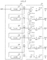
- FIG. 1 is a diagram illustrating a configuration of a semiconductor system 100 in accordance with an embodiment.
- the semiconductor system 100 may include a host 200 and a semiconductor apparatus 300 .
- the semiconductor apparatus 300 may include a memory area, a fail information control circuit 303 , a repair circuit 304 , an ECC circuit 306 , and input/output pads 305 .
- the memory area may include a normal memory cell array 301 and a redundancy memory cell array 302 .
- the redundancy memory cell array 302 may include redundancy memory cells for repairing unusable memory cells (hereinafter, referred to as failed cells) among memory cells of the normal memory cell array 301 .
- the fail information control circuit 303 may classify detected fails into a case where write data has a first value (for example, ‘0’) and a case where the write data has a second value (for example, ‘1’), according to a result of comparing the write data with read data for each address, and count the classified fails to generate counting signals.
- a first value for example, ‘0’
- a second value for example, ‘1’
- the semiconductor apparatus 300 may perform the aforementioned counting signal generation operation on at least one of the normal memory cell array 301 and the redundancy memory cell array 302 .
- a fail detected when the write data is ‘0’ is referred to as a first fail
- a signal according to the first fail is referred to as a first fail discrimination signal
- a fail detected when the write data is ‘1’ is referred to as a second fail and a signal according to the second fail is referred to as a second fail discrimination signal.
- the fail information control circuit 303 may generate a counting correction signal by correcting a value of the counting signal.
- Write data provided to the fail information control circuit 303 may be data (for example, 0 or 1) having a predetermined pattern for a test.
- Read data provided to the fail information control circuit 303 may be data read from the normal memory cell array 301 for each address.
- the fail information control circuit 303 may output a value of ‘1’ of the counting signal as a counting signal corrected by resetting the remaining bits except for the most significant bit of bits, which is described below with reference to FIG. 6 .
- the repair circuit 304 may include a one-time programmable (OTP) memory 311 and a program circuit 312 .
- OTP one-time programmable
- the OTP memory 311 may include an electrical fuse (e-fuse) array such that a repair operation is possible after the packaging of the semiconductor apparatus 300 as well as before the packaging thereof.
- e-fuse electrical fuse
- the OTP memory 311 may store an address for accessing an unusable normal memory cell, that is, a failed cell, of the normal memory cell array in the e-fuse array.
- the program circuit 312 may program a failed address into the OTP memory 311 .
- the program circuit 312 may program the failed address by selectively rupturing fuses of the OTP memory 311 .
- the fuse rupture operation is an operation in which a high voltage is applied to an e-fuse array to destroy a gate insulating layer of a transistor constituting the e-fuse array, and failed address programming is feasible by performing a selective rupture operation on a plurality of e-fuses according to a value of the failed address.
- the repair circuit 304 may control an operation of programming the failed address into the OTP memory 311 and an operation of accessing an address corresponding to a redundancy memory cell instead of the failed address when an address provided from an exterior is the failed address during a normal operation.
- the ECC circuit 306 may perform a correction operation using an error correction code on input/output data of the semiconductor apparatus 300 .
- the input/output pads 305 may include data input/output pads DQ.
- the host 200 may be, for example, a test device, provide the semiconductor apparatus 300 with a command, an address, and/or write data, and determine the pass or fail of a normal memory cell and/or a redundancy memory cell corresponding to an address according to read data outputted from the semiconductor apparatus 300 .
- a fail flag may define the number of fail bits according to a timing at which the fail flag is generated, which is described below.
- the counting signal, the corrected counting signal, and the fail flag may be used as information on the number of fail bits of read data.
- FIG. 2 is a diagram illustrating a configuration of the fail information control circuit in accordance with an embodiment.
- the fail information control circuit 303 may include a comparison circuit 401 , a fail bit discrimination circuit 403 , and a fail information output circuit 405 .
- the comparison circuit 401 may generate a comparison result signal CMP by comparing read data RDATA and write data WDATA.
- the write data WDATA may be inputted as a random or predetermined pattern (for example, all ‘0’ or all ‘1’), that is, a pattern promised in advance between the host 200 and the semiconductor apparatus 300 .
- the comparison circuit 401 may include an exclusive OR logic (XOR).
- the exclusive OR logic (XOR) compares the read data RDATA and the write data WDATA by one bit unit. When the read data RDATA and the write data WDATA coincide with each other, the exclusive OR logic (XOR) may output the comparison result signal CMP at a low level, and when the read data RDATA and the write data WDATA do not coincide with each other, the exclusive OR logic (XOR) may output the comparison result signal CMP at a high level.
- the comparison result signal CMP When the comparison result signal CMP is at a high level, it may indicate that a fail bit has occurred due to an error of a corresponding memory cell.
- the fail bit discrimination circuit 403 may generate a first fail discrimination signal FL 0 and a second fail discrimination signal FL 1 according to the write data WDATA in response to the comparison result signal CMP.
- the first fail discrimination signal FL 0 may indicate that a detected fail has occurred when the write data is ‘0’.
- the second fail discrimination signal FL 1 may indicate that the detected fail has occurred when the write data is ‘1’.
- the fail information output circuit 405 may be configured to generate a first counting signal Aa ⁇ 0:K> and a second counting signal Ab ⁇ 0:K> by counting the first fail discrimination signal FL 0 and the second fail discrimination signal FL 1 , and generate a first counting correction signal Qa ⁇ 0:K> and a second counting correction signal Qb ⁇ 0:K> by resetting the remaining bits except for the most significant bit of a first level among the bits of the first counting signal Aa ⁇ 0:K> and the second counting signal Ab ⁇ 0:K>.
- the fail information output circuit 405 may include a fail bit counter 600 and a counting signal correction circuit 700 .
- the fail bit counter 600 may generate the first counting signal Aa ⁇ 0:K> by counting the first fail discrimination signal FL 0 and generate the second counting signal Ab ⁇ 0:K> by counting the second fail discrimination signal FL 1 .
- the counting signal correction circuit 700 may output, as the first counting correction signal Qa ⁇ 0:K>, a signal obtained by resetting the levels of the remaining bits, except for the most significant bit among the high level bits of the first counting signal Aa ⁇ 0:K>, to a low level.
- the counting signal correction circuit 700 may output, as the second counting correction signal Qb ⁇ 0:K>, a signal obtained by resetting the levels of the remaining bits, except for the most significant bit among the high level bits of the second counting signal Ab ⁇ 0:K>, to a low level.
- FIG. 3 is a diagram illustrating a configuration of the fail bit discrimination circuit 403 of FIG. 2 .
- the fail bit discrimination circuit 403 may include a first logic gate 501 , a second logic gate 502 , and a third logic gate 503 .
- the first logic gate 501 may invert and output the write data WDATA.
- the second logic gate 502 may output the second fail discrimination signal FL 1 by performing a logical AND operation on the comparison result signal CMP and the write data WDATA.
- the third logic gate 503 may output the first fail discrimination signal FL 0 by performing a logical AND operation on the comparison result signal CMP and the output signal of the first logic gate 501 .
- the first counting signal Aa ⁇ 0:K> and the second counting signal Ab ⁇ 0:K> may be generated through test operations illustrated in FIG. 4 to FIG. 7 .
- FIG. 4 and FIG. 5 are diagrams illustrating examples of test operations for each address
- FIG. 6 and FIG. 7 are diagrams illustrating examples of test operations for substantially the same address.
- the test operation may be performed by a first method, for example, a bit by bit method.
- the bit by bit method may be a method of counting a fail bit by repeating write and read in units of bits while changing Address #0 to #9.
- test data may be ‘0’ or ‘1’ during each write operation.
- a fail bit related to ‘0’ that is, the first fail discrimination signal FL 0 may be generated.
- the value of the first counting signal Aa ⁇ 0:K> may increase to be ‘1’ and the second counting signal Ab ⁇ 0:K> may substantially maintain an initial value ‘0’.
- a fail bit related to ‘1’ that is, the second fail discrimination signal FL 1 may be generated.
- the value of the first counting signal Aa ⁇ 0:K> may be substantially maintained to ‘1’ and the value of the second counting signal Ab ⁇ 0:K> may increase to be ‘1’.
- the fail bit related to ‘0’ that is, the first fail discrimination signal FL 0 may be generated.
- the value of the first counting signal Aa ⁇ 0:K> may increase to ‘2’ and the value of the second counting signal Ab ⁇ 0:K> may be substantially maintained to ‘1’.
- the fail bit related to ‘0’ that is, the first fail discrimination signal FL 0 may be generated.
- the value of the first counting signal Aa ⁇ 0: K> may increase to ‘4’ and the value of the second counting signal Ab ⁇ 0:K> may be substantially maintained to ‘2’.
- the test operation may be performed by a second method, for example, an all by all method.
- the all by all method may be a method of dividing addresses into a plurality of groups, writing substantially the same data to each group, and then performing sequential read and fail bit counting. Data written to different groups may be different.
- Address #0 to Address #14 data ‘0’ may be written to Address #0 to Address #4 and then sequential read and fail bit counting may be performed, data ‘1’ may be written to Address #5 to Address #9 and then sequential read and fail bit counting may be performed, and data ‘0’ may be written to Address #10 to Address #14 and then sequential read and fail bit counting may be performed.
- first fail discrimination signals FL 0 are generated and the value of the first counting signal Aa ⁇ 0:K> may become ‘4’, and two second fail discrimination signals FL 1 are generated and the value of the second counting signal Ab ⁇ 0:K> may be substantially maintained to ‘2’.
- the test operation may be performed by a third method, for example, a method of writing substantially the same data to substantially the same address and then performing read and fail bit counting.
- data ‘0’ may be written to Address #0 and then read and fail bit counting may be performed.
- FIG. 6 and FIG. 7 illustrate merely examples in which data ‘0’ is written, and data ‘1’ may be written.
- the value of the first counting signal Aa ⁇ 0:K> and the value of the second counting signal Ab ⁇ 0:K> are equal to or less than predetermined reference values that may be determined differently to match the characteristics of a semiconductor circuit, it may be determined as a soft error, and when the values exceed the predetermined reference values, it may be determined as a hard error.
- the case of FIG. 6 may be determined as the soft error, and when the case is determined as the soft error, an ECC correction operation may be performed.
- the case of FIG. 7 may be determined as the hard error because a relatively larger number of fail bits may be generated than FIG. 6 , and when the case is determined as the hard error, a repair operation may be performed to repair a failed cell with a redundancy cell.
- FIG. 8 and FIG. 9 are diagrams illustrating configurations of the fail bit counter and the counting signal correction circuit of FIG. 2 .
- the first counting circuit 610 may include a plurality of unit counters 611 to 616 .
- the plurality of unit counters 611 to 616 may be configured to generate the first counting signal Aa ⁇ 0:5> by counting the comparison result signal CMP or the output Aa 0 , Aa 1 , Aa 2 , Aa 3 , and Aa 4 of the counters of previous sequences.
- the first correction circuit 710 may include a plurality of inverters 711 - 1 and 712 - 1 to 712 - 6 , a plurality of NAND gates 711 - 2 to 711 - 6 , and a plurality of AND gates 713 - 1 to 713 - 4 .
- the first inverter 711 - 1 may output a signal Ba 5 obtained by inverting Aa 5 of the first counting signal Aa ⁇ 0:5>.
- the second inverter 712 - 1 may invert the signal Ba 5 and output the inverted signal as Qa 5 of the first counting correction signal Qa ⁇ 0:5>.
- the first NAND gate 711 - 2 may output a signal Ba 4 obtained by performing a logical inverse AND operation on Aa 4 of the first counting signal Aa ⁇ 0:5> and the signal Ba 5 .
- the third inverter 712 - 2 may invert the signal Ba 4 and output the inverted signal as Qa 4 of the first counting correction signal Qa ⁇ 0:5>.
- the first AND gate 713 - 1 may output a signal Ca 1 obtained by performing a logical AND operation on the signal Ba 4 and the signal Ba 5 .
- the second NAND gate 711 - 3 may output a signal Ba 3 obtained by performing a logical inverse AND operation on Aa 3 of the first counting signal Aa ⁇ 0:5> and the signal Ca 1 .
- the fourth inverter 712 - 3 may invert the signal Ba 3 and output the inverted signal as Qa 3 of the first counting correction signal Qa ⁇ 0:5>.
- the second AND gate 713 - 2 may output a signal Ca 2 obtained by performing a logical AND operation on the signal Ba 3 and the signal Ca 1 .
- the third NAND gate 711 - 4 may output a signal Ba 2 obtained by performing a logical inverse AND operation on Aa 2 of the first counting signal Aa ⁇ 0:5> and the signal Ca 2 .
- the fifth inverter 712 - 4 may invert the signal Ba 2 and output the inverted signal as Qa 2 of the first counting correction signal Qa ⁇ 0:5>.
- the third AND gate 713 - 3 may output a signal Ca 3 obtained by performing a logical AND operation on the signal Ba 2 and the signal Ca 2 .
- the fourth NAND gate 711 - 5 may output a signal Ba 1 obtained by performing a logical inverse AND operation on Aa 1 of the first counting signal Aa ⁇ 0:5> and the signal Ca 3 .
- the sixth inverter 712 - 5 may invert the signal Ba 1 and output the inverted signal as Qa 1 of the first counting correction signal Qa ⁇ 0:5>.
- the fourth AND gate 713 - 4 may output a signal Ca 4 obtained by performing a logical AND operation on the signal Ba 1 and the signal Ca 3 .
- the fifth NAND gate 711 - 6 may output a signal Ba 0 obtained by performing a logical inverse AND operation on Aa 0 of the first counting signal Aa ⁇ 0:5> and the signal Ca 4 .
- the seventh inverter 712 - 6 may invert the signal Ba 0 and output the inverted signal as Qa 0 of the first counting correction signal Qa ⁇ 0:5>.
- the logics of the first correction circuit 710 may output, as the first counting correction signal Qa ⁇ 0:5>, ‘001000’, which is a value obtained by resetting the remaining bits Aa 0 and Aa 1 , except for the most significant bit Aa 2 of the bits Aa ⁇ 0:2>, having a value of ‘1’, of Aa ⁇ 0:5>, to ‘0’.
- the first counting circuit 620 may include a plurality of unit counters 621 to 626 .
- the plurality of unit counters 621 to 626 may be configured to generate the second counting signal Ab ⁇ 0:5> by counting the comparison result signal CMP or the output Ab 0 , Ab 1 , Ab 2 , Ab 3 , and Ab 4 of the counters of previous sequences.
- the second correction circuit 720 may include a plurality of inverters 721 - 1 and 722 - 1 to 722 - 6 , a plurality of NAND gates 721 - 2 to 721 - 6 , and a plurality of AND gates 723 - 1 to 723 - 4 .
- the first inverter 721 - 1 may output a signal Bb 5 obtained by inverting Ab 5 of the second counting signal Ab ⁇ 0:5>.
- the second inverter 722 - 1 may invert the signal Bb 5 and output the inverted signal as Qb 5 of the second counting correction signal Qb ⁇ 0:5>.
- the first NAND gate 721 - 2 may output a signal Bb 4 obtained by performing a logical inverse AND operation on Ab 4 of the second counting signal Ab ⁇ 0:5> and the signal Bb 5 .
- the third inverter 722 - 2 may invert the signal Bb 4 and output the inverted signal as Qb 4 of the second counting correction signal Qb ⁇ 0:5>.
- the first AND gate 723 - 1 may output a signal Cb 1 obtained by performing a logical AND operation on the signal Bb 4 and the signal Bb 5 .
- the second NAND gate 721 - 3 may output a signal Bb 3 obtained by performing a logical inverse AND operation on Ab 3 of the second counting signal Ab ⁇ 0:5> and the signal Cb 1 .
- the fourth inverter 722 - 3 may invert the signal Bb 3 and output the inverted signal as Qb 3 of the second counting correction signal Qb ⁇ 0:5>.
- the second AND gate 723 - 2 may output a signal Cb 2 obtained by performing a logical AND operation on the signal Bb 3 and the signal Cb 1 .
- the third NAND gate 721 - 4 may output a signal Bb 2 obtained by performing a logical inverse AND operation on Ab 2 of the second counting signal Ab ⁇ 0:5> and the signal Cb 2 .
- the fifth inverter 722 - 4 may invert the signal Bb 2 and output the inverted signal as Qb 2 of the second counting correction signal Qb ⁇ 0:5>.
- the third AND gate 723 - 3 may output a signal Cb 3 obtained by performing a logical AND operation on the signal Bb 1 and the signal Cb 2 .
- the fourth NAND gate 721 - 5 may output a signal Bb 1 obtained by performing a logical inverse AND operation on Ab 1 of the second counting signal Ab ⁇ 0:5> and the signal Cb 3 .
- the sixth inverter 722 - 5 may invert the signal Bb 1 and output the inverted signal as Qb 1 of the second counting correction signal Qb ⁇ 0:5>.
- the fourth AND gate 723 - 4 may output a signal Cb 4 obtained by performing a logical AND operation on the signal Bb 1 and the signal Cb 3 .
- the fifth NAND gate 721 - 6 may output a signal Bb 0 obtained by performing a logical inverse AND operation on Ab 0 of the second counting signal Ab ⁇ 0:5> and the signal Cb 4 .
- the seventh inverter 722 - 6 may invert the signal Bb 0 and output the inverted signal as Qb 0 of the second counting correction signal Qb ⁇ 0:5>.
- the logics of the second correction circuit 720 may output, as the second counting correction signal Qb ⁇ 0:5>, ‘010000’, which is a value obtained by resetting the remaining bits Ab 0 , except for the most significant bit Ab 1 of the bits Ab ⁇ 0:1>, having a value of ‘1’, of Ab ⁇ 0:5>, to ‘0’.
- FIG. 10 and FIG. 11 are diagrams for explaining a fail flag output method in accordance with an embodiment.
- the semiconductor apparatus 300 in accordance with an embodiment may provide the host 200 with a first fail flag using the first counting correction signal Qa ⁇ 0:K> and a second fail flag using the second counting correction signal Qb ⁇ 0:K>, which have been described with reference to FIG. 8 and FIG. 9 .
- the semiconductor apparatus 300 may provide the host 200 with the first fail flag and the second fail flag through the data input/output pads DQ.
- BL burst length
- the first counting correction signal Qa ⁇ 0:K> may be used as the first fail flag.
- DQ 1 burst length
- the second counting correction signal Qb ⁇ 0:K> may be used as the second fail flag.
- the first counting correction signal Qa ⁇ 0:K> which is generated by resetting the remaining bits, except for the most significant bit among the bits, having a value of ‘1’, of the first counting signal Aa ⁇ 0:K>, to ‘0’ by using the first correction circuit 710 , may be included in DQ 0 /BL ⁇ 0:5> as the first fail flag and provided to the host 200 .
- the second counting correction signal Qb ⁇ 0:K> which is generated by resetting the remaining bits, except for the most significant bit among the bits, having a value of ‘1’, of the second counting signal Ab ⁇ 0:K>, to ‘0’ by using the second correction circuit 720 , may be included in DQ 1 /BL ⁇ 0:5> as the second fail flag and provided to the host 200 .
- Qa 0 of the first counting correction signal Qa ⁇ 0:K> may represent a binary number 2 0 , it may be defined that one first fail discrimination signal FL 0 has been generated by putting high level Qa 0 into BL 0 .
- Qa 1 may represent 2 1 +2 0 , it may be defined that 2 to 3 first fail discrimination signals FL 0 have been generated by putting high level Qa 1 into BL 1 .
- Qa 2 may represent 2 2 +2 1 +2 0 , it may be defined that 4 to 7 first fail discrimination signals FL 0 have been generated by putting high level Qa 2 into BL 2 .
- first fail discrimination signals FL 0 have been generated by putting high level Qa 3 into BL 3
- 16 to 31 first fail discrimination signals FL 0 have been generated by putting high level Qa 4 into BL 4
- 32 to 63 first fail discrimination signals FL 0 have been generated by putting high level Qa 5 into BL 5 .
- Qb 0 of the second counting correction signal Qb ⁇ 0:K> may represent a binary number 2 0 , it may be defined that one second fail discrimination signal FL 1 has been generated by putting high level Qb 0 into BL 0 .
- Qb 1 may represent 2 1 +2 0 , it may be defined that 2 to 3 second fail discrimination signals FL 1 have been generated by putting high level Qb 1 into BL 1 .
- Qb 2 may represent 2 2 +2 1 +2 0 , it may be defined that 4 to 7 second fail discrimination signals FL 1 have been generated by putting high level Qb 2 into BL 2 .
- 8 to 15 second fail discrimination signals FL 1 have been generated by putting high level Qb 3 into BL 3
- 16 to 31 second fail discrimination signals FL 1 have been generated by putting high level Qb 4 into BL 4
- 32 to 63 second fail discrimination signals FL 1 have been generated by putting high level Qb 5 into BL 5 .
- the first counting correction signal Qa ⁇ 0:5> at a low level is allocated to BL ⁇ 0:5>
- the first fail discrimination signal FL 0 has not been generated
- the second counting correction signal Qb ⁇ 0:5> at a low level is allocated to BL ⁇ 0:5>
- the second fail discrimination signal FL 1 has not been generated.
- the aforementioned example is merely an example in which the first counting correction signal Qa ⁇ 0:5> is allocated to DQ 0 /BL ⁇ 0:5> as the first fail flag and the second counting correction signal Qb ⁇ 0:5> is allocated to DQ 1 /BL ⁇ 0:5> as the second fail flag, DQ of another sequence may also be used, and in the case of a circuit configuration of increasing the number of bits of a signal in which fail bits have been counted, the generation of a larger number of fail bits may be defined.
- FIG. 12 is a diagram illustrating an example of the fail flag output method according to FIG. 10 and FIG. 11 .
- the first fail flag according to the high level Qa 2 may be generated at a timing corresponding to BL 2 of BL ⁇ 0:5>, which may define that 4 to 7 fail bits have been generated, referring to FIG. 12 .
- the second fail flag according to the high level Qb 1 may be generated at a timing corresponding to BL 1 of BL ⁇ 0:5>, which may define that 2 to 3 fail bits have been generated, referring to FIG. 12 .
- FIG. 13 is a flowchart illustrating a fail information control method in accordance with an embodiment.
- a test data write and scan operation S 101 and a fail bit counting operation S 102 may be performed.
- the fail bit counting may include a series of steps S 103 to S 107 .
- step S 103 when the write data WDATA and the read data RDATA do not coincide with each other, the type of a fail bit is determined, that is, it is determined whether the write data WDATA is ‘0’ (S 104 ).
- step S 104 when the write data WDATA is ‘0’, a ‘0’ fail count value, that is, the value of the first counting signal Aa ⁇ 0:K> is increased (S 105 ).
- step S 104 when the write data WDATA is not ‘0’, a ‘1’ fail count value, that is, the value of the second counting signal Ab ⁇ 0:K> is increased (S 106 ).
- step S 105 or step S 106 it is determined whether the fail bit counting has ended (S 107 ).
- step S 107 when the fail bit counting has not ended, the fail bit counting may be performed for another address or substantially the same address.
- step S 107 when the fail bit counting for all addresses has ended, fail bit count values may be outputted (S 108 ).
- Step S 108 may include an operation in which the first counting signal Aa ⁇ 0:K> and the second counting signal Ab ⁇ 0:K> are outputted to an exterior of the semiconductor apparatus 300 , for example, the host 200 , as the fail bit count values.
- Step S 108 may include an operation in which the first fail flag using the first counting correction signal Qa ⁇ 0:K> and the second fail flag using the second counting correction signal Qb ⁇ 0:K> are outputted to an exterior of the semiconductor apparatus 300 , for example, the host 200 , as the fail bit count values.
- the host 200 may determine that an error detected in the semiconductor apparatus 300 is a soft error or a hard error according to the fail bit count value (S 109 ).
- the host 200 may allow the ECC correction to be performed, and when it is determined that the error detected in the semiconductor apparatus 300 is the hard error, the host 200 may allow the repair operation of replacing a failed cell with a redundancy cell to be performed (S 110 ).
- the fail bit count values outputted from the semiconductor apparatus 300 are values obtained by discriminating a fail bit related to ‘0’ data or a fail bit related to ‘1’ data.
Landscapes
- Engineering & Computer Science (AREA)
- Theoretical Computer Science (AREA)
- Quality & Reliability (AREA)
- Physics & Mathematics (AREA)
- General Engineering & Computer Science (AREA)
- General Physics & Mathematics (AREA)
- For Increasing The Reliability Of Semiconductor Memories (AREA)
Abstract
Description
Claims (17)
Applications Claiming Priority (2)
| Application Number | Priority Date | Filing Date | Title |
|---|---|---|---|
| KR10-2019-0080055 | 2019-07-03 | ||
| KR1020190080055A KR102790220B1 (en) | 2019-07-03 | 2019-07-03 | Fail information control circuit, semiconductor apparatus including the same and fail information control method of the semiconductor apparatus |
Publications (2)
| Publication Number | Publication Date |
|---|---|
| US20210004285A1 US20210004285A1 (en) | 2021-01-07 |
| US11307919B2 true US11307919B2 (en) | 2022-04-19 |
Family
ID=73919513
Family Applications (1)
| Application Number | Title | Priority Date | Filing Date |
|---|---|---|---|
| US16/709,273 Active 2040-04-01 US11307919B2 (en) | 2019-07-03 | 2019-12-10 | Fail information control circuit, semiconductor apparatus including the same, and fail information control method of semiconductor apparatus |
Country Status (3)
| Country | Link |
|---|---|
| US (1) | US11307919B2 (en) |
| KR (1) | KR102790220B1 (en) |
| CN (1) | CN112185454B (en) |
Citations (8)
| Publication number | Priority date | Publication date | Assignee | Title |
|---|---|---|---|---|
| KR100933861B1 (en) | 2008-03-10 | 2009-12-24 | 주식회사 하이닉스반도체 | Nonvolatile Memory Device and Program Verification Method |
| US20120254686A1 (en) * | 2010-10-01 | 2012-10-04 | SIGLEAD Inc. | Non-volatile semiconductor memory devices and error correction methods |
| US20170091026A1 (en) * | 2015-09-29 | 2017-03-30 | Apple Inc. | Storing Address of Spare in Failed Memory Location |
| US20170206124A1 (en) * | 2016-01-15 | 2017-07-20 | Bong-Soon Lim | Operating method of non-volatile memory device |
| US9778985B1 (en) * | 2016-08-17 | 2017-10-03 | SK Hynix Inc. | Operating method of data storage device |
| US20180144813A1 (en) * | 2016-11-21 | 2018-05-24 | SK Hynix Inc. | Fail bit counter and semiconductor memory device having the same |
| US20190130991A1 (en) * | 2017-11-02 | 2019-05-02 | Samsung Electronics Co., Ltd. | Semiconductor memory devices, memory systems and methods of operating semiconductor memory devices |
| US20200183784A1 (en) * | 2018-12-11 | 2020-06-11 | Samsung Electronics Co., Ltd. | Nonvolatile memory device and memory system including nonvolatile memory device |
Family Cites Families (8)
| Publication number | Priority date | Publication date | Assignee | Title |
|---|---|---|---|---|
| EP2003653B1 (en) * | 2006-04-06 | 2010-08-04 | Advantest Corporation | Test device and test method |
| WO2008038710A1 (en) * | 2006-09-28 | 2008-04-03 | Mitsubishi Electric Corporation | Fault detector, fault detection method, and fault detection program |
| JP2009059434A (en) * | 2007-08-31 | 2009-03-19 | Toshiba Corp | Semiconductor integrated circuit |
| US9235466B2 (en) * | 2012-07-03 | 2016-01-12 | Samsung Electronics Co., Ltd. | Memory devices with selective error correction code |
| KR20170054182A (en) * | 2015-11-09 | 2017-05-17 | 에스케이하이닉스 주식회사 | Semiconductor device |
| KR102517700B1 (en) * | 2016-06-10 | 2023-04-05 | 에스케이하이닉스 주식회사 | Semiconductor memory device and operating method thereof |
| KR102692010B1 (en) * | 2016-10-06 | 2024-08-05 | 에스케이하이닉스 주식회사 | Semiconductor device for executing a test method checking a cell allay failure |
| KR20180104455A (en) * | 2017-03-13 | 2018-09-21 | 에스케이하이닉스 주식회사 | Repair device and semiconductor including the same |
-
2019
- 2019-07-03 KR KR1020190080055A patent/KR102790220B1/en active Active
- 2019-12-10 US US16/709,273 patent/US11307919B2/en active Active
-
2020
- 2020-01-08 CN CN202010017650.2A patent/CN112185454B/en active Active
Patent Citations (8)
| Publication number | Priority date | Publication date | Assignee | Title |
|---|---|---|---|---|
| KR100933861B1 (en) | 2008-03-10 | 2009-12-24 | 주식회사 하이닉스반도체 | Nonvolatile Memory Device and Program Verification Method |
| US20120254686A1 (en) * | 2010-10-01 | 2012-10-04 | SIGLEAD Inc. | Non-volatile semiconductor memory devices and error correction methods |
| US20170091026A1 (en) * | 2015-09-29 | 2017-03-30 | Apple Inc. | Storing Address of Spare in Failed Memory Location |
| US20170206124A1 (en) * | 2016-01-15 | 2017-07-20 | Bong-Soon Lim | Operating method of non-volatile memory device |
| US9778985B1 (en) * | 2016-08-17 | 2017-10-03 | SK Hynix Inc. | Operating method of data storage device |
| US20180144813A1 (en) * | 2016-11-21 | 2018-05-24 | SK Hynix Inc. | Fail bit counter and semiconductor memory device having the same |
| US20190130991A1 (en) * | 2017-11-02 | 2019-05-02 | Samsung Electronics Co., Ltd. | Semiconductor memory devices, memory systems and methods of operating semiconductor memory devices |
| US20200183784A1 (en) * | 2018-12-11 | 2020-06-11 | Samsung Electronics Co., Ltd. | Nonvolatile memory device and memory system including nonvolatile memory device |
Non-Patent Citations (1)
| Title |
|---|
| Google Scholar/Patents—text refined (Year: 2021). * |
Also Published As
| Publication number | Publication date |
|---|---|
| KR102790220B1 (en) | 2025-04-03 |
| US20210004285A1 (en) | 2021-01-07 |
| CN112185454B (en) | 2024-02-23 |
| KR20210004135A (en) | 2021-01-13 |
| CN112185454A (en) | 2021-01-05 |
Similar Documents
| Publication | Publication Date | Title |
|---|---|---|
| CN112420116B (en) | Apparatus and method for fuse error detection | |
| CN108877870B (en) | Repair circuit for repair operation and memory device including repair circuit | |
| US9959164B2 (en) | Semiconductor device and driving method thereof | |
| US11328787B2 (en) | One-time programmable memory circuit and semiconductor apparatus including the same | |
| US8634260B2 (en) | Semiconductor device and control method therefor | |
| US9104588B2 (en) | Circuits, apparatuses, and methods for address scrambling | |
| US20140126302A1 (en) | Memory device and test method thereof | |
| US7137049B2 (en) | Method and apparatus for masking known fails during memory tests readouts | |
| US7231582B2 (en) | Method and system to encode and decode wide data words | |
| US10338984B2 (en) | Storage control apparatus, storage apparatus, and storage control method | |
| US8867288B2 (en) | Memory device and test method thereof | |
| US11243828B2 (en) | Semiconductor apparatus and semiconductor system including the semiconductor apparatus | |
| KR20180038211A (en) | Fuse circuit, repair control circuit and semiconductor apparatus including the same | |
| US11532375B2 (en) | Latch circuit and memory device including the same | |
| US9847142B2 (en) | Semiconductor apparatus and repair method thereof | |
| CN100498975C (en) | Semiconductor memory device and semiconductor memory device testing method | |
| US10535418B2 (en) | Memory device including repair circuit and operation method thereof | |
| US11307919B2 (en) | Fail information control circuit, semiconductor apparatus including the same, and fail information control method of semiconductor apparatus | |
| KR20190075354A (en) | Memory device and operation method of the same | |
| US11574699B2 (en) | Semiconductor device equipped with global column redundancy | |
| US10102921B1 (en) | Fuse blowing method and fuse blowing system |
Legal Events
| Date | Code | Title | Description |
|---|---|---|---|
| AS | Assignment |
Owner name: SK HYNIX INC., KOREA, REPUBLIC OF Free format text: ASSIGNMENT OF ASSIGNORS INTEREST;ASSIGNOR:KANG, JAE YONG;REEL/FRAME:051234/0869 Effective date: 20191205 |
|
| FEPP | Fee payment procedure |
Free format text: ENTITY STATUS SET TO UNDISCOUNTED (ORIGINAL EVENT CODE: BIG.); ENTITY STATUS OF PATENT OWNER: LARGE ENTITY |
|
| STPP | Information on status: patent application and granting procedure in general |
Free format text: DOCKETED NEW CASE - READY FOR EXAMINATION |
|
| STPP | Information on status: patent application and granting procedure in general |
Free format text: NON FINAL ACTION MAILED |
|
| STPP | Information on status: patent application and granting procedure in general |
Free format text: RESPONSE TO NON-FINAL OFFICE ACTION ENTERED AND FORWARDED TO EXAMINER |
|
| STPP | Information on status: patent application and granting procedure in general |
Free format text: FINAL REJECTION MAILED |
|
| STPP | Information on status: patent application and granting procedure in general |
Free format text: NOTICE OF ALLOWANCE MAILED -- APPLICATION RECEIVED IN OFFICE OF PUBLICATIONS |
|
| STPP | Information on status: patent application and granting procedure in general |
Free format text: PUBLICATIONS -- ISSUE FEE PAYMENT VERIFIED |
|
| STCF | Information on status: patent grant |
Free format text: PATENTED CASE |
|
| MAFP | Maintenance fee payment |
Free format text: PAYMENT OF MAINTENANCE FEE, 4TH YEAR, LARGE ENTITY (ORIGINAL EVENT CODE: M1551); ENTITY STATUS OF PATENT OWNER: LARGE ENTITY Year of fee payment: 4 |