US11295949B2 - Virtual wafer techniques for fabricating semiconductor devices - Google Patents
Virtual wafer techniques for fabricating semiconductor devices Download PDFInfo
- Publication number
- US11295949B2 US11295949B2 US16/372,381 US201916372381A US11295949B2 US 11295949 B2 US11295949 B2 US 11295949B2 US 201916372381 A US201916372381 A US 201916372381A US 11295949 B2 US11295949 B2 US 11295949B2
- Authority
- US
- United States
- Prior art keywords
- doped
- semiconductor substrate
- crystalline
- heavily
- regions
- Prior art date
- Legal status (The legal status is an assumption and is not a legal conclusion. Google has not performed a legal analysis and makes no representation as to the accuracy of the status listed.)
- Active
Links
Images


Classifications
-
- H10P95/11—
-
- H—ELECTRICITY
- H10—SEMICONDUCTOR DEVICES; ELECTRIC SOLID-STATE DEVICES NOT OTHERWISE PROVIDED FOR
- H10D—INORGANIC ELECTRIC SEMICONDUCTOR DEVICES
- H10D30/00—Field-effect transistors [FET]
- H10D30/01—Manufacture or treatment
- H10D30/021—Manufacture or treatment of FETs having insulated gates [IGFET]
- H10D30/028—Manufacture or treatment of FETs having insulated gates [IGFET] of double-diffused metal oxide semiconductor [DMOS] FETs
- H10D30/0291—Manufacture or treatment of FETs having insulated gates [IGFET] of double-diffused metal oxide semiconductor [DMOS] FETs of vertical DMOS [VDMOS] FETs
- H10D30/0297—Manufacture or treatment of FETs having insulated gates [IGFET] of double-diffused metal oxide semiconductor [DMOS] FETs of vertical DMOS [VDMOS] FETs using recessing of the gate electrodes, e.g. to form trench gate electrodes
-
- H—ELECTRICITY
- H10—SEMICONDUCTOR DEVICES; ELECTRIC SOLID-STATE DEVICES NOT OTHERWISE PROVIDED FOR
- H10D—INORGANIC ELECTRIC SEMICONDUCTOR DEVICES
- H10D30/00—Field-effect transistors [FET]
- H10D30/01—Manufacture or treatment
- H10D30/021—Manufacture or treatment of FETs having insulated gates [IGFET]
- H10D30/025—Manufacture or treatment of FETs having insulated gates [IGFET] of vertical IGFETs
-
- H—ELECTRICITY
- H01—ELECTRIC ELEMENTS
- H01L—SEMICONDUCTOR DEVICES NOT COVERED BY CLASS H10
- H01L21/00—Processes or apparatus adapted for the manufacture or treatment of semiconductor or solid state devices or of parts thereof
- H01L21/02—Manufacture or treatment of semiconductor devices or of parts thereof
- H01L21/02104—Forming layers
- H01L21/02365—Forming inorganic semiconducting materials on a substrate
- H01L21/02367—Substrates
- H01L21/0237—Materials
- H01L21/02373—Group 14 semiconducting materials
- H01L21/02381—Silicon, silicon germanium, germanium
-
- H10P14/2905—
-
- H—ELECTRICITY
- H01—ELECTRIC ELEMENTS
- H01L—SEMICONDUCTOR DEVICES NOT COVERED BY CLASS H10
- H01L21/00—Processes or apparatus adapted for the manufacture or treatment of semiconductor or solid state devices or of parts thereof
- H01L21/02—Manufacture or treatment of semiconductor devices or of parts thereof
- H01L21/02104—Forming layers
- H01L21/02365—Forming inorganic semiconducting materials on a substrate
- H01L21/02518—Deposited layers
- H01L21/02521—Materials
- H01L21/02524—Group 14 semiconducting materials
- H01L21/02532—Silicon, silicon germanium, germanium
-
- H—ELECTRICITY
- H01—ELECTRIC ELEMENTS
- H01L—SEMICONDUCTOR DEVICES NOT COVERED BY CLASS H10
- H01L21/00—Processes or apparatus adapted for the manufacture or treatment of semiconductor or solid state devices or of parts thereof
- H01L21/02—Manufacture or treatment of semiconductor devices or of parts thereof
- H01L21/02104—Forming layers
- H01L21/02365—Forming inorganic semiconducting materials on a substrate
- H01L21/02518—Deposited layers
- H01L21/0257—Doping during depositing
- H01L21/02573—Conductivity type
- H01L21/02576—N-type
-
- H—ELECTRICITY
- H01—ELECTRIC ELEMENTS
- H01L—SEMICONDUCTOR DEVICES NOT COVERED BY CLASS H10
- H01L21/00—Processes or apparatus adapted for the manufacture or treatment of semiconductor or solid state devices or of parts thereof
- H01L21/02—Manufacture or treatment of semiconductor devices or of parts thereof
- H01L21/02104—Forming layers
- H01L21/02365—Forming inorganic semiconducting materials on a substrate
- H01L21/02612—Formation types
- H01L21/02617—Deposition types
- H01L21/02634—Homoepitaxy
-
- H—ELECTRICITY
- H01—ELECTRIC ELEMENTS
- H01L—SEMICONDUCTOR DEVICES NOT COVERED BY CLASS H10
- H01L21/00—Processes or apparatus adapted for the manufacture or treatment of semiconductor or solid state devices or of parts thereof
- H01L21/02—Manufacture or treatment of semiconductor devices or of parts thereof
- H01L21/02104—Forming layers
- H01L21/02365—Forming inorganic semiconducting materials on a substrate
- H01L21/02656—Special treatments
- H01L21/02664—Aftertreatments
-
- H—ELECTRICITY
- H01—ELECTRIC ELEMENTS
- H01L—SEMICONDUCTOR DEVICES NOT COVERED BY CLASS H10
- H01L21/00—Processes or apparatus adapted for the manufacture or treatment of semiconductor or solid state devices or of parts thereof
- H01L21/67—Apparatus specially adapted for handling semiconductor or electric solid state devices during manufacture or treatment thereof; Apparatus specially adapted for handling wafers during manufacture or treatment of semiconductor or electric solid state devices or components ; Apparatus not specifically provided for elsewhere
- H01L21/683—Apparatus specially adapted for handling semiconductor or electric solid state devices during manufacture or treatment thereof; Apparatus specially adapted for handling wafers during manufacture or treatment of semiconductor or electric solid state devices or components ; Apparatus not specifically provided for elsewhere for supporting or gripping
- H01L21/6835—Apparatus specially adapted for handling semiconductor or electric solid state devices during manufacture or treatment thereof; Apparatus specially adapted for handling wafers during manufacture or treatment of semiconductor or electric solid state devices or components ; Apparatus not specifically provided for elsewhere for supporting or gripping using temporarily an auxiliary support
-
- H01L29/045—
-
- H01L29/66734—
-
- H—ELECTRICITY
- H10—SEMICONDUCTOR DEVICES; ELECTRIC SOLID-STATE DEVICES NOT OTHERWISE PROVIDED FOR
- H10D—INORGANIC ELECTRIC SEMICONDUCTOR DEVICES
- H10D30/00—Field-effect transistors [FET]
- H10D30/60—Insulated-gate field-effect transistors [IGFET]
- H10D30/64—Double-diffused metal-oxide semiconductor [DMOS] FETs
- H10D30/66—Vertical DMOS [VDMOS] FETs
- H10D30/668—Vertical DMOS [VDMOS] FETs having trench gate electrodes, e.g. UMOS transistors
-
- H—ELECTRICITY
- H10—SEMICONDUCTOR DEVICES; ELECTRIC SOLID-STATE DEVICES NOT OTHERWISE PROVIDED FOR
- H10D—INORGANIC ELECTRIC SEMICONDUCTOR DEVICES
- H10D62/00—Semiconductor bodies, or regions thereof, of devices having potential barriers
- H10D62/10—Shapes, relative sizes or dispositions of the regions of the semiconductor bodies; Shapes of the semiconductor bodies
- H10D62/124—Shapes, relative sizes or dispositions of the regions of semiconductor bodies or of junctions between the regions
-
- H—ELECTRICITY
- H10—SEMICONDUCTOR DEVICES; ELECTRIC SOLID-STATE DEVICES NOT OTHERWISE PROVIDED FOR
- H10D—INORGANIC ELECTRIC SEMICONDUCTOR DEVICES
- H10D62/00—Semiconductor bodies, or regions thereof, of devices having potential barriers
- H10D62/10—Shapes, relative sizes or dispositions of the regions of the semiconductor bodies; Shapes of the semiconductor bodies
- H10D62/13—Semiconductor regions connected to electrodes carrying current to be rectified, amplified or switched, e.g. source or drain regions
- H10D62/149—Source or drain regions of field-effect devices
- H10D62/151—Source or drain regions of field-effect devices of IGFETs
- H10D62/156—Drain regions of DMOS transistors
- H10D62/157—Impurity concentrations or distributions
-
- H—ELECTRICITY
- H10—SEMICONDUCTOR DEVICES; ELECTRIC SOLID-STATE DEVICES NOT OTHERWISE PROVIDED FOR
- H10D—INORGANIC ELECTRIC SEMICONDUCTOR DEVICES
- H10D62/00—Semiconductor bodies, or regions thereof, of devices having potential barriers
- H10D62/40—Crystalline structures
- H10D62/405—Orientations of crystalline planes
-
- H—ELECTRICITY
- H10—SEMICONDUCTOR DEVICES; ELECTRIC SOLID-STATE DEVICES NOT OTHERWISE PROVIDED FOR
- H10D—INORGANIC ELECTRIC SEMICONDUCTOR DEVICES
- H10D62/00—Semiconductor bodies, or regions thereof, of devices having potential barriers
- H10D62/80—Semiconductor bodies, or regions thereof, of devices having potential barriers characterised by the materials
- H10D62/83—Semiconductor bodies, or regions thereof, of devices having potential barriers characterised by the materials being Group IV materials, e.g. B-doped Si or undoped Ge
-
- H10P14/20—
-
- H10P14/24—
-
- H10P14/2924—
-
- H10P14/3211—
-
- H10P14/3246—
-
- H10P14/3411—
-
- H10P14/3442—
-
- H10P14/3452—
-
- H10P14/38—
-
- H10P14/3802—
-
- H10P32/15—
-
- H10P52/00—
-
- H10P72/74—
-
- H—ELECTRICITY
- H01—ELECTRIC ELEMENTS
- H01L—SEMICONDUCTOR DEVICES NOT COVERED BY CLASS H10
- H01L2221/00—Processes or apparatus adapted for the manufacture or treatment of semiconductor or solid state devices or of parts thereof covered by H01L21/00
- H01L2221/67—Apparatus for handling semiconductor or electric solid state devices during manufacture or treatment thereof; Apparatus for handling wafers during manufacture or treatment of semiconductor or electric solid state devices or components; Apparatus not specifically provided for elsewhere
- H01L2221/683—Apparatus for handling semiconductor or electric solid state devices during manufacture or treatment thereof; Apparatus for handling wafers during manufacture or treatment of semiconductor or electric solid state devices or components; Apparatus not specifically provided for elsewhere for supporting or gripping
- H01L2221/68304—Apparatus for handling semiconductor or electric solid state devices during manufacture or treatment thereof; Apparatus for handling wafers during manufacture or treatment of semiconductor or electric solid state devices or components; Apparatus not specifically provided for elsewhere for supporting or gripping using temporarily an auxiliary support
- H01L2221/6835—Apparatus for handling semiconductor or electric solid state devices during manufacture or treatment thereof; Apparatus for handling wafers during manufacture or treatment of semiconductor or electric solid state devices or components; Apparatus not specifically provided for elsewhere for supporting or gripping using temporarily an auxiliary support used as a support during build up manufacturing of active devices
-
- H—ELECTRICITY
- H01—ELECTRIC ELEMENTS
- H01L—SEMICONDUCTOR DEVICES NOT COVERED BY CLASS H10
- H01L2221/00—Processes or apparatus adapted for the manufacture or treatment of semiconductor or solid state devices or of parts thereof covered by H01L21/00
- H01L2221/67—Apparatus for handling semiconductor or electric solid state devices during manufacture or treatment thereof; Apparatus for handling wafers during manufacture or treatment of semiconductor or electric solid state devices or components; Apparatus not specifically provided for elsewhere
- H01L2221/683—Apparatus for handling semiconductor or electric solid state devices during manufacture or treatment thereof; Apparatus for handling wafers during manufacture or treatment of semiconductor or electric solid state devices or components; Apparatus not specifically provided for elsewhere for supporting or gripping
- H01L2221/68304—Apparatus for handling semiconductor or electric solid state devices during manufacture or treatment thereof; Apparatus for handling wafers during manufacture or treatment of semiconductor or electric solid state devices or components; Apparatus not specifically provided for elsewhere for supporting or gripping using temporarily an auxiliary support
- H01L2221/68381—Details of chemical or physical process used for separating the auxiliary support from a device or wafer
-
- H10P72/7426—
-
- H10P72/744—
Definitions
- the power transistor can include a single transistor occupying most of a semiconductor die.
- the power transistor is utilized to conduct relatively large currents, and therefore utilizes a heavily doped semiconductor substrate, which reduces the bulk resistance of the semiconductor substrate.
- donor impurity atoms such as Boron (B) or Phosphorous (P)
- molten intrinsic semiconductor material such as Silicon (Si)
- Si Silicon
- the resulting ingot can then be sliced into a plurality of semiconductor wafers.
- small traces of Oxygen (O) can be present in the reaction chamber or introduced by the phosphorous doping source. The oxygen atoms can conglomerate with the excess phosphorus to form defects in the semiconductor lattice structure.
- the semiconductor device fabrication process can require the use of a heavily n-doped semiconductor substrate 110 , such as silicon heavily doped with phosphorous.
- the silicon substrate heavily doped with phosphorous utilized in the commercial fabrication of semiconductor devices, can have one or more types of point defects 120 , 130 within the lattice structure of the semiconductor substrate 110 , as illustrated in FIG. 1A .
- phosphorous and oxygen can combine as Phosphorus Pentoxide (P 2 O 5 ) and generate point defects in the semiconductor substrate 110 .
- Point defects at or near the surface of the semiconductor substrate 110 can cause a reduction of the breakdown voltage and or excessive leakage current in the one or more devices fabricated on the substrate.
- Other dopants, such as Arsenic (As) can result in similar point defect based voltage breakdown failure mechanisms and or excessive leakage current.
- TMOSFETs Trench Metal Oxide Semiconductor Field Effect Transistors
- VMOS Vertical MOSFET
- VDMOS Vertical Diffused MOSFET
- DMOS Double-Diffused MOSFET
- UMOS Power MOSFET
- a method of fabricating a semiconductor device can include depositing a heavily doped crystalline substrate on a lightly doped crystalline virtual substrate. One or more regions of one or more devices can be formed in and on the heavily doped crystalline substrate. The lightly doped crystalline virtual substrate can then be removed leaving the one or more regions of the one or more devices formed in and on the heavily doped crystalline substrate.
- a method of fabricating a semiconductor device can include epitaxially depositing a heavily n-doped substrate layer on a lightly n-doped virtual substrate. One or more regions of one or more devices can be formed about a surface of the heavily n-doped substrate layer. The lightly n-doped virtual substrate can be removed from the heavily n-doped substrate after forming the one or more regions of the one or more devices.
- a method of fabricating a semiconductor device can include depositing a buffer layer on a crystalline virtual substrate.
- a heavily doped crystalline substrate can then be deposited on the buffer layer.
- the butter layer can be configured to prevent propagation of defects from the crystalline virtual substrate into the heavily doped crystalline substrate.
- One or more regions of one or more device can be formed about the surface of the heavily doped crystalline substrate before the crystalline virtual substrate and optionally the buffer layer are removed.
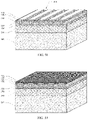
- FIGS. 1A and 1B show an exemplary semiconductor device fabrication process, in accordance with the conventional art.
- FIG. 2 shows a method of fabricating a semiconductor device, in accordance with aspects of the present technology.
- FIGS. 3A, 3B and 3C show an exemplary semiconductor device fabrication process, in accordance with aspects of the present technology.
- FIGS. 4A and 4B show a method of fabricating a vertical power device, in accordance with aspects of the present technology.
- FIGS. 5A through 5K show an exemplary vertical power device fabrication process, in accordance with aspects of the present technology.
- FIGS. 6A and 6B show a method of fabricating a vertical power device, in accordance with aspects of the present technology.
- FIGS. 7A through 7K show an exemplary vertical power device fabrication process, in accordance with aspects of the present technology.
- routines, modules, logic blocks, and other symbolic representations of operations on data within one or more electronic devices are presented in terms of routines, modules, logic blocks, and other symbolic representations of operations on data within one or more electronic devices.
- the descriptions and representations are the means used by those skilled in the art to most effectively convey the substance of their work to others skilled in the art.
- a routine, module, logic block and/or the like is herein, and generally, conceived to be a self-consistent sequence of processes or instructions leading to a desired result.
- the processes are those including physical manipulations of physical quantities.
- these physical manipulations take the form of electric or magnetic signals capable of being stored, transferred, compared and otherwise manipulated in an electronic device.
- these signals are referred to as data, bits, values, elements, symbols, characters, terms, numbers, strings, and/or the like with reference to embodiments of the present technology.
- the use of the disjunctive is intended to include the conjunctive.
- the use of definite or indefinite articles is not intended to indicate cardinality.
- a reference to “the” object or “a” object is intended to denote also one of a possible plurality of such objects. It is also to be understood that the phraseology and terminology used herein is for the purpose of description and should not be regarded as limiting.
- the method of fabricating a semiconductor device can include optionally depositing a barrier layer (not shown) on a lightly doped crystalline virtual substrate 310 , at 210 .
- the barrier layer can be configured to reduce doping diffusion from a subsequently described heavily doped crystalline substrate layer 310 to the lightly doped crystalline virtual substrate 320 .
- a heavily doped crystalline substrate layer 320 can be deposited on the lightly doped crystalline virtual substrate 310 , or on the barrier layer if included.
- the term virtual substrate is used herein to convey that the virtual substrate is used to deposit the heavily doped crystalline substrate layer thereupon, and then is subsequently removed before fabrication of the semiconductor device is completed, as further described below.
- the lightly doped crystalline virtual substrate 310 can be substantially free of point defects.
- the lightly doped crystalline virtual substrate 310 can be a silicon wafer lightly doped with phosphorous.
- the silicon wafer lightly doped with phosphorous can have a wafer thickness of approximately 625 micrometers ( ⁇ m) and a resistivity of approximately a few milli-Ohms centimeter (m ⁇ cm) or less.
- the silicon wafer lightly doped with phosphorous can have a very low point defect density.
- a silicon wafer used in the conventional art of comparable cost that is heavily doped with phosphorous, with a resistivity below m ⁇ cm can have a substantially higher point defect density due to the precipitation of oxygen atoms with the abundantly present phosphorus in the substrate.
- the heavily doped crystalline substrate 320 can be formed by epitaxially depositing silicon in the presence of phosphorous doping utilizing Chemical Vapor Deposition, Vapor-Phase Epitaxy (VPE), Liquid- Phase Epitaxy (LPE), Molecular Beam Epitaxy (MBE), or other similar epitaxy process.
- VPE Vapor-Phase Epitaxy
- LPE Liquid- Phase Epitaxy
- MBE Molecular Beam Epitaxy
- a gas of Silicon Tetrachloride (SiCh 4 ), Silane (SilH 4 ), dichlorosilane (SiH 2 C 2 ), trichlorosilane (SiHCl 3 ) or the like, along with an impurity gas of Phosphine (PH 3 ) or the like can be used in VPE at a temperature of approximately 1200° Celsius (C) to deposit a silicon epitaxy layer heavily doped with phosphorous on the silicon lightly doped with phosphorous virtual substrate.
- the epitaxial process can be performed to deposit a silicon epitaxial layer heavily doped with phosphorus to a resistivity of less than 1 m ⁇ cm, and a thickness of approximately 20-50 ⁇ m, on the silicon lightly doped with phosphorous virtual substrate.
- the heavily doped crystalline substrate layer 320 deposited on the lightly doped crystalline virtual substrate 310 can optionally be annealed to reduce one or more types of defects in the heavily doped crystalline substrate layer 320 .
- the silicon lightly doped with phosphorous virtual substrate and the epitaxially deposited silicon heavily doped with phosphorous can be subjected to a thermal cycle of approximately 1000° C. to reduce one or more types of defects in the deposited silicon heavily doped with phosphorus substrate layer.
- one or more regions of one or more devices 330 can be formed about an exposed surface of the heavily doped crystalline substrate layer 320 .
- one or more semiconductor fabrication techniques such as epitaxial deposition, photolithography, etching, implanting, deposition, and the like can be performed to form one or more regions of one or more devices 330 , such as drain regions, drift regions, body regions, source regions, gate regions, gate dielectric regions, contacts, vias and or the like of one or more transistors or other similar devices, in and on the surface of the deposited silicon heavily doped with phosphorus substrate layer.
- the lightly doped crystalline virtual substrate 310 can be removed from the heavily doped crystalline substrate layer 320 leaving the one or more regions of the one or more devices 330 formed about the heavily doped crystalline substrate layer 320 .
- the lightly doped crystalline virtual substrate 3310 can be removed by a back grinding and polishing process.
- the heavily doped crystalline substrate layer 320 can optionally be thinned.
- the back grinding and polishing process can also be utilized to remove a portion of the heavily doped crystalline substrate layer 320 from the exposed surface opposite the one or more region of the one or more devices 330 .
- the heavily doped crystalline substrate layer 320 can be thinned to a final thickness of approximately 20-50 ⁇ m.
- the method of fabricating a semiconductor device can proceed with forming one or more additional regions of the one or more devices 330 about the exposed surface of the heavily doped crystalline substrate layer 320 .
- one or more additional semiconductor fabrication techniques such as photolithography, etching, implanting, deposition, and the like can be performed to form one or more regions of one or more devices 330 , such as encapsulation layers, leads and or the like of one or more transistors or other similar devices, in and on the surface of the heavily doped crystalline substrate layer.
- FIGS. 4A and 4B a method of fabricating an exemplary vertical power device, in accordance with aspects of the present technology, is shown.
- the fabrication method will be further described with reference to FIGS. 5A through 5K , which show portions of an exemplary vertical power device during various stages of fabricating.
- the vertical power device in one implementation, can be a Trench Metal Oxide Semiconductor Field Effect Transistor (TMOSFET).
- TMOSFET Trench Metal Oxide Semiconductor Field Effect Transistor
- the method of fabricating a vertical power device can include optionally depositing a barrier layer (not shown) on a lightly n-doped virtual substrate 502 , at 405 .
- the barrier layer can be configured to reduce doping diffusion from a subsequently described heavily doped crystalline substrate layer 504 to the lightly doped crystalline virtual substrate 502 .
- the barrier layer can be a thin layer of Arsenic (As) or Phosphorus (P).
- a heavily n-doped substrate layer 504 can be epitaxially deposited on a lightly n-doped crystalline virtual substrate 502 or the optional buffer layer.
- virtual substrate is used herein to convey that the virtual substrate is used to epitaxially grow the heavily doped crystalline substrate layer thereupon, and then is subsequently removed from the finished semiconductor device as further described below.
- the lightly n-doped crystalline virtual substrate 502 can be substantially free of point defects.
- the lightly n-doped crystalline virtual substrate 502 can be a silicon wafer lightly doped with phosphorous.
- the silicon wafer lightly doped with phosphorous can have a wafer thickness of approximately 625 ⁇ m and a resistivity of approximately a few milli-Ohms centimeter (m ⁇ cm) or less.
- m ⁇ cm milli-Ohms centimeter
- a silicon wafer of comparable cost that is heavily doped with phosphorous, with a resistivity below 1 (m ⁇ cm) can have a substantially higher point defect density due to the precipitation of oxygen atoms with the abundantly present phosphorus in the substrate.
- the heavily n-doped crystalline substrate 504 can be formed by epitaxially depositing silicon in the presence of phosphorous doping utilizing Chemical Vapor Deposition, Vapor-Phase Epitaxy (VPE), Liquid- Phase Epitaxy (LPE), Molecular Beam Epitaxy (MBE), or other similar epitaxy process.
- VPE Vapor-Phase Epitaxy
- LPE Liquid- Phase Epitaxy
- MBE Molecular Beam Epitaxy
- a gas of Silicon Tetrachloride (SiCl 4 ), Silane (SiH 4 ), dichlorosilane (SiH 2 Cl 2 ), trichlorosilane (SiHCl 3 ) or the like, along with an impurity gas of Phosphine (PH 3 ) or the like can be used in VPE at a temperature of approximately 1200° C. to deposit a silicon epitaxy layer heavily doped with phosphorous on the silicon lightly doped with phosphorous virtual substrate.
- an Arsenic (As) buffer layer can be deposited on the lightly n-doped crystalline virtual substrate 502 before the heavily n-doped crystalline substrate 504 is epitaxially deposited to control out-diffusion of the n-doping form the heavily n-doped crystalline substrate 504 to the lightly n-doped crystalline virtual substrate 502 to improve control of the doping concentration and or doping profile in the heavily n-doped crystalline substrate 504 .
- the epitaxial process can be performed to deposit a silicon epitaxial layer heavily doped with phosphorus to a resistivity of less than 1 m ⁇ m, and a thickness of approximately 20-50 ⁇ m on the silicon lightly doped with phosphorous virtual substrate.
- a moderately n-doped crystalline layer 506 can be epitaxially deposited on the heavily n-doped substrate layer 504 .
- the moderately n-doped crystalline layer can be configured to be a drift region.
- the moderately n-doped crystalline layer can be an epitaxially deposited silicon layer moderately doped with Phosphorous (P).
- the heavily n-doped crystalline substrate layer 504 and the moderately n-doped drift region 506 can optionally be annealed to reduce one or more types of defects in the heavily n-doped crystalline substrate layer 504 and the moderately n-doped drift region 506 .
- the silicon lightly doped with phosphorous virtual substrate 502 , the epitaxial deposited silicon heavily doped with phosphorous substrate 504 and the epitaxial deposited silicon moderately doped with phosphorous drift region 506 can be subjected to a thermal cycle of approximately 1000° C. to reduce one or more types of defects in the epitaxial deposited silicon heavily doped with phosphorus substrate layer 504 and epitaxial deposited silicon moderately doped with phosphorous drift region 506 .
- a plurality of trenches 508 can be formed in the moderately n-doped drift region 506 .
- a mask layer can be deposited and patterned utilizing a photolithograph process.
- the moderately n-doped crystalline drift layer 506 exposed by the patterned mask layer 510 can be etched to form the plurality of trenches 508 , as illustrated in FIG. 5B .
- the patterned mask layer 510 can then be removed after the plurality of trenches 508 have been etched.
- a plurality of gate dielectric regions can be formed on the walls of the plurality of trenches 508 .
- a plurality of gate regions can also be formed in the plurality of trenches 508 , at 435 .
- the plurality of gate dielectric regions can be disposed between the moderately n-doped crystalline drift region 506 and the plurality of gate regions.
- a gate dielectric layer 512 can be grown on the exposed surface of the moderately n-doped crystalline drift region 506 utilizing a thermal oxidation process to form a silicon oxide layer.
- a conformal n-doped semiconductor layer 514 can be deposited in the trenches 506 and on top of the gate dielectric layer 512 .
- the n-doped semiconductor layer 514 can be a polysilicon layer doped with phosphorous.
- the n-doped semiconductor layer 514 and the gate dielectric layer 512 can then be etched back until the n-doped semiconductor and the gate dielectric are removed from the surface of the moderately n-doped crystalline drift region 506 leaving the gate dielectric and the n-doped semiconductor filling the trenches 508 to form the plurality of gate regions 516 , and the plurality of gate dielectric regions 518 disposed between the moderately n-doped crystalline drift region 506 and the plurality of gate regions 516 , as illustrated in FIG. 5E .
- a plurality of p-doped body regions 520 can be formed in a portion of the moderately n-doped drift region 506 , opposite the heavily n-doped crystalline substrate layer 504 .
- a mask layer can be deposited and patterned utilizing a photolithography process.
- the plurality of p-doped body regions 520 can be formed by implanting a p-dopant, such as Boron (B), 524 into an upper portion of the moderately n-doped crystalline drift region 506 exposed by the patterned mask 522 .
- the patterned mask 522 can then be removed after implanting the plurality of p-doped body regions 520 .
- the plurality of p-doped body regions 520 can extend to the bottom of the plurality of gate regions 516 .
- a plurality of n-doped source regions 526 can be formed in a portion of the plurality of p-doped body regions 520 opposite the moderately n-doped crystalline drift region 506 .
- a mask layer 528 can be deposited and patterned utilizing a photolithography process.
- the plurality of n-doped source regions 526 can be formed by implanting a n-dopant, such as phosphorous, 530 into an upper portion of the p-doped body regions 520 exposed by the patterned mask 528 .
- the patterned mask 528 can then be removed after implanting the plurality of n-doped source regions 526 .
- a source-body contact coupled to the plurality of n-doped source regions 526 and the plurality of p-doped body regions 520 can be formed.
- a dielectric layer 532 can be deposited over the surface of the plurality of gate regions 516 , the plurality of gate dielectric regions 518 , the plurality of source regions 526 and the plurality of body regions 520 .
- a mask layer 534 can be deposited and patterned utilizing a photolithography process. The portions of the dielectric layer 532 exposed by the patterned mask layer 534 can be selectively etched to form a plurality of source-body contact openings 536 in the dielectric layer 530 .
- the patterned mask 534 can then be removed after forming the source-body contact openings 536 in the dielectric layer 532 .
- a source-body contact layer 538 can be deposited in the source-body contact openings 536 and over the surface of the patterned dielectric layer 532 .
- the source-body-contact layer 538 can be patterned to form a plurality of source-body contacts 540 coupled to the to the plurality of n-doped source regions 526 and the plurality of p-doped body regions 520 .
- the lightly n-doped crystalline virtual substrate 502 can be removed from the heavily n-doped crystalline substrate layer 504 leaving the plurality of gate regions 516 , the plurality of gate dielectric regions 518 , the plurality of p-doped body regions 520 , and the plurality of source-body contacts 540 formed about the moderately n-doped crystalline drift region 506 .
- the lightly n-doped crystalline virtual substrate 502 can be removed by a back grinding and polishing process.
- the heavily n-doped crystalline substrate layer 504 can optionally be thinned.
- the back grinding and polishing process can also be utilized to remove a portion of the heavily n-doped crystalline substrate layer 504 from the exposed surface opposite the plurality of gate regions 516 , the plurality of gate dielectric regions 518 , the plurality of p-doped body regions 520 , and the plurality of source-body contacts 540 formed about the moderately n-doped crystalline drift region 506 .
- the heavily doped crystalline substrate layer 504 can be thinned to a final thickness of approximately 25-50 micrometers ( ⁇ m).
- the heavily doped crystalline substrate 504 can be thinned to achieve a resistivity of approximately 1 m ⁇ cm or less.
- the method of fabricating a semiconductor device can proceed with forming one or more additional regions of the one or more devices about the heavily n-doped crystalline substrate layer 504 .
- one or more additional semiconductor fabrication techniques such as photolithography, etching, implanting, deposition, and the like can be performed to form one or more regions of one or more devices, such as encapsulation layers, leads and or the like of one or more transistors or other similar devices, in and on the surface of the epitaxial deposited heavily n-doped substrate layer.
- a drain contact layer 542 can be deposited on the heavily n-doped crystalline substrate layer 504 opposite the plurality of gate regions 516 , the plurality of gate dielectric regions 518 , the plurality of source regions 526 and the plurality of body regions 520 . Additional processes can be performed to form gate contacts, encapsulation layers, and the like.
- the exemplary semiconductor device and method of manufacture thereof described and illustrated with reference to FIGS. 4A-4B and FIGS. 5A-5K is included herein to teach the implementation of aspects of the present technology.
- the present technology is not limited thereto and can be readily applied to any number of different semiconductor devices and methods of manufacturing such semiconductor devices.
- FIGS. 6A and 6B a method of fabricating another exemplary vertical power device, in accordance with aspects of the present technology, is shown.
- the fabrication method will be further described with reference to FIGS. 7A through 7K , which show portions of an exemplary vertical power device during various stage of fabricating.
- the vertical power device in one implementation, can be a Trench Metal Oxide Semiconductor Field Effect Transistor (TMOSFET).
- the method of fabricating a vertical power device can include depositing a barrier layer 702 on a crystalline virtual substrate 704 , at 605 .
- the crystalline virtual substrate 704 can be of any type and can have defects therein.
- the barrier layer 702 can be configured to prevent propagation of defects from the virtual substrate 704 into a subsequently described heavily doped crystalline substrate layer 706 .
- the barrier layer can be a thin layer of Arsenic (As) or Phosphorus (P).
- a heavily n-doped substrate layer 706 can be epitaxially deposited on the buffer layer 702 .
- virtual substrate is used herein to convey that the virtual substrate is used to epitaxially grow the heavily doped crystalline substrate layer thereupon, and then is subsequently removed from the finished semiconductor device as further described below.
- the crystalline virtual substrate 704 can be a silicon wafer doped with phosphorous.
- the silicon wafer doped with phosphorous can have a wafer thickness of approximately 625 ⁇ m and a resistivity of approximately a few milli-Ohms centimeter (m ⁇ cm) or less.
- the heavily n-doped crystalline substrate 706 can be formed by epitaxially depositing silicon in the presence of phosphorous doping utilizing Chemical Vapor Deposition, Vapor-Phase Epitaxy (VPE), Liquid- Phase Epitaxy (LPE), Molecular Beam Epitaxy (MBE), or other similar epitaxy process.
- VPE Vapor-Phase Epitaxy
- LPE Liquid- Phase Epitaxy
- MBE Molecular Beam Epitaxy
- a gas of Silicon Tetrachloride (SiCl 4 ), Silane (SiH 4 ), dichlorosilane (SiH 2 Cl 2 ), trichlorosilane (SiHCl 3 ) or the like, along with an impurity gas of Phosphine (PH 3 ) or the like can be used in VPE at a temperature of approximately 1200° C. to deposit a silicon epitaxy layer heavily doped with phosphorous on the buffer layer 702 .
- the epitaxial process can be performed to deposit a silicon epitaxial layer heavily doped with phosphorus to a resistivity of less than 1 (m ⁇ cm), and a thickness of approximately 20-50 ⁇ m on the buffer layer 702 .
- a moderately n-doped crystalline layer 708 can be epitaxially deposited on the heavily n-doped substrate layer 706 .
- the moderately n-doped crystalline layer can be configured to be a drift region.
- the moderately n-doped crystalline layer can be an epitaxially deposited silicon layer moderately doped with Phosphorous (P).
- the heavily n-doped crystalline substrate layer 706 and the moderately n-doped drift region 708 can optionally be annealed to reduce one or more types of defects in the heavily n-doped crystalline substrate layer 706 and the moderately n-doped drift region 708 .
- the silicon doped with phosphorous virtual substrate 704 , the buffer layer 702 , the epitaxial deposited silicon heavily doped with phosphorous substrate 706 and the epitaxial deposited silicon moderately doped with phosphorous drift region 708 can be subjected to a thermal cycle of approximately 1000° C. to reduce one or more types of defects in the epitaxial deposited silicon heavily doped with phosphorus substrate layer 706 and epitaxial deposited silicon moderately doped with phosphorous drift region 708 .
- a plurality of trenches 710 can be formed in the moderately n-doped drift region 708 .
- a mask layer can be deposited and patterned utilizing a photolithograph process.
- the moderately n-doped crystalline drift layer 708 exposed by the patterned mask layer 712 can be etched to form the plurality of trenches 710 , as illustrated in FIG. 7B .
- the patterned mask layer 712 can then be removed after the plurality of trendies 710 have been etched.
- a plurality of gate dielectric regions can be formed on the walls of the plurality of trenches 710 .
- a plurality of gate regions can also be formed in the plurality of trenches 710 , at 635 .
- the plurality of gate dielectric regions can be disposed between the moderately n-doped crystalline drift region 708 and the plurality of gate regions.
- a gate dielectric layer 714 can be grown on the exposed surface of the moderately n-doped crystalline drift region 708 utilizing a thermal oxidation process to form a silicon oxide layer.
- a conformal n-doped semiconductor layer 716 can be deposited in the trenches 708 and on top of the gate dielectric layer 714 .
- the n-doped semiconductor layer 716 can be a polysilicon layer doped with phosphorous.
- the n-doped semiconductor layer 716 and the gate dielectric layer 714 can then be etched back until the n-doped semiconductor and the gate dielectric are removed from the surface of the moderately n-doped crystalline drift region 70 S leaving the gate dielectric and the n-doped semiconductor filling the trenches 710 to form the plurality of gate regions 718 , and the plurality of gate dielectric regions 720 disposed between the moderately n-doped crystalline drift region 708 and the plurality of gate regions 718 , as illustrated in FIG. 7E .
- a plurality of p-doped body regions 722 can be formed in a portion of the moderately n-doped drift region 708 , opposite the heavily n-doped crystalline substrate layer 706 .
- a mask layer can be deposited and patterned utilizing a photolithography process.
- the plurality of p-doped body regions 722 can be formed by implanting a p-dopant, such as Boron (B), 726 into an upper portion of the moderately n-doped crystalline drift region 708 exposed by the patterned mask 724 .
- the patterned mask 724 can then be removed after implanting the plurality of p-doped body regions 722 .
- the plurality of p-doped body regions 722 can extend to the bottom of the plurality of gate regions 718 .
- a plurality of n-doped source regions 728 can be formed in a portion of the plurality of p-doped body regions 722 opposite the moderately n-doped crystalline drift region 708 .
- a mask layer 730 can be deposited and patterned utilizing a photolithography process.
- the plurality of n-doped source regions 728 can be formed by implanting a n-dopant, such as phosphorous, 732 into an upper portion of the p-doped body regions 722 exposed by the patterned mask 730 .
- the patterned mask 730 can then be removed after implanting the plurality of n-doped source regions 728 .
- a source-body contact coupled to the plurality of n-doped source regions 728 and the plurality of p-doped body regions 722 can be formed.
- a dielectric layer 734 can be deposited over the surface of the plurality of gate regions 718 , the plurality of gate dielectric regions 720 , the plurality of source regions 728 and the plurality of body regions 722 .
- a mask layer 736 can be deposited and patterned utilizing a photolithography process. The portions of the dielectric layer 734 exposed by the patterned mask layer 736 can be selectively etched to form a plurality of source-body contact openings 738 in the dielectric layer 732 .
- the patterned mask 736 can then be removed after forming the source-body contact openings 738 in the dielectric layer 734 .
- a source-body contact layer 740 can be deposited in the source-body contact openings 738 and over the surface of the patterned dielectric layer 734 .
- the source-body-contact layer 740 can be patterned to form a plurality of source-body contacts 742 coupled to the to the plurality of n-doped source regions 728 and the plurality of p-doped body regions 722 .
- the crystalline virtual substrate 704 can be removed.
- the buffer layer 702 can also be removed from the heavily n-doped crystalline substrate layer 706 , leaving the plurality of gate regions 718 , the plurality of gate dielectric regions 720 , the plurality of p-doped body regions 722 , and the plurality of source-body contacts 742 formed about the moderately n-doped crystalline drift region 708 .
- the crystalline virtual substrate 704 and buffer layer 702 can be removed by a back grinding and polishing process.
- the heavily n-doped crystalline substrate layer 706 can optionally be thinned.
- the back grinding and polishing process can also be utilized to remove a portion of the heavily n-doped crystalline substrate layer 706 from the exposed surface opposite the plurality of gate regions 718 , the plurality of gate dielectric regions 720 , the plurality of p-doped body regions 722 , and the plurality of source-body contacts 742 formed about the moderately n-doped crystalline drift region 708 .
- the heavily doped crystalline substrate layer 706 can be thinned to a final thickness of approximately 25-50 micrometers ( ⁇ m).
- the heavily doped crystalline substrate 706 can be thinned to achieve a resistivity of approximately 1 m ⁇ cm or less.
- the method of fabricating a semiconductor device can proceed with forming one or more additional regions of the one or more devices about the heavily n-doped crystalline substrate layer 706 .
- one or more additional semiconductor fabrication techniques such as photolithography, etching, implanting, deposition, and the like can be performed to form one or more regions of one or more devices, such as encapsulation layers, leads and or the like of one or more transistors or other similar devices, in and on the surface of the epitaxial deposited heavily n-doped substrate layer.
- a drain contact layer 744 can be deposited on the heavily n-doped crystalline substrate layer 706 opposite the plurality of gate regions 718 , the plurality of gate dielectric regions 720 , the plurality of source regions 728 and the plurality of body regions 722 . Additional processes can be performed to form gate contacts, encapsulation layers, and the like.
- the exemplary semiconductor device and method of manufacture thereof described and illustrated with reference to FIGS. 6A-6B and FIGS. 7A-7K is included herein to teach the implementation of aspects of the present technology.
- the present technology is not limited thereto and can be readily applied to any number of different semiconductor devices and methods of manufacturing such semiconductor devices.
- the heavily doped crystalline substrate 320 , 504 , 706 is characterized by a low bulk resistivity and a low point defect concentration.
- the low bulk resistivity is particularly advantageous for use in Trench MOSFETs (TMOSFETs), Vertical MOSFET (VMOS), Vertical Diffused MOSFET (VDMOS), Double-Diffused (DMOS), Power MOSFET (UMOS), and other similar devices that conduct relatively large amounts of currently through the substrate.
- the low bulk resistivity of the heavily doped crystalline substrate 320 , 502 , 706 results in a relatively low on resistance of such Trench MOSFETs (TMOSFETs), Vertical MOSFET (VMOS), Vertical Diffused MOSFET (VDMOS), Double-Diffused (DMOS), Power MOSFET (UMOS), and other similar devices.
- TMOSFETs Trench MOSFETs
- VMOS Vertical MOSFET
- VDMOS Vertical Diffused MOSFET
- DMOS Double-Diffused
- UMOS Power MOSFET
- Trench MOSFETs Trench MOSFETs
- VMOS Vertical MOSFET
- VDMOS Vertical Diffused MOSFET
- DMOS Double-Diffused MOSFET
- UMOS Power MOSFET
- a lateral transistor architecture where the conduction channel is along the surface of the substrate is typically affected only by point defects proximate the surface of the substrate and not those located down in the substrate away from the active region of the later transistor architecture.
- the low point defect concentration of the heavily doped crystalline substrate 320 , 504 , 706 results in a lower breakdown voltage failure rate and or lower leakage current for Trench MOSFETs (TMOSFETs), Vertical MOSFET (VMOS), Vertical Diffused MOSFET (VDMOS), Double-Diffused (DMOS), Power MOSFET (UMOS), and other similar devices.
- TMOSFETs Trench MOSFETs
- VMOS Vertical MOSFET
- VDMOS Vertical Diffused MOSFET
- DMOS Double-Diffused
- UMOS Power MOSFET
- the technique of epitaxially depositing a heavily doped crystalline substrate layer on a lightly doped crystalline virtual substrate advantageously enables the use of a lightly doped crystalline wafer which is less expensive than a heavily doped crystalline wafer.
- the density of point defects in a lightly doped crystalline wafer is substantially lower than the density of point defect in a heavily doped crystalline wafer for wafers of approximately the same costs.
- the point defect density has been found to have a one-to-one relationship to the breakdown voltage failure mode in devices fabricated in the wafer.
- the process of epitaxially depositing a heavily doped crystalline substrate layer on a lightly doped crystalline virtual substrate advantageously provides for a reduction in the breakdown voltage failure mode in devices fabricated in the wafer, as compared to fabricating the devices in a heavily doped crystalline substrate wafer.
- the subsequent removal of the lightly doped crystalline virtual substrate also advantageously enables the devices fabricated in the epitaxially deposited heavily doped crystalline substrate layer to achieve on-resistance values comparable to heavily doped crystalline substrates wafer.
- the epitaxial deposition of the heavily doped crystalline substrate layer also advantageously enables increased control of the doping profile and or thickness of the epitaxial heavily doped crystalline substrate layer and or additional regions formed in or on the epitaxial heavily doped crystalline substrate layer.
Landscapes
- Engineering & Computer Science (AREA)
- Microelectronics & Electronic Packaging (AREA)
- Condensed Matter Physics & Semiconductors (AREA)
- General Physics & Mathematics (AREA)
- Manufacturing & Machinery (AREA)
- Computer Hardware Design (AREA)
- Physics & Mathematics (AREA)
- Power Engineering (AREA)
- Chemical & Material Sciences (AREA)
- Materials Engineering (AREA)
- Metal-Oxide And Bipolar Metal-Oxide Semiconductor Integrated Circuits (AREA)
- Recrystallisation Techniques (AREA)
- Crystallography & Structural Chemistry (AREA)
Abstract
Description
Claims (18)
Priority Applications (4)
| Application Number | Priority Date | Filing Date | Title |
|---|---|---|---|
| US16/372,381 US11295949B2 (en) | 2019-04-01 | 2019-04-01 | Virtual wafer techniques for fabricating semiconductor devices |
| CN202010237984.0A CN111799174A (en) | 2019-04-01 | 2020-03-30 | Virtual Wafer Technology for Manufacturing Semiconductor Devices |
| EP20167151.8A EP3730676A3 (en) | 2019-04-01 | 2020-03-31 | Virtual wafer techniques for fabricating semiconductor devices |
| KR1020200039589A KR102435904B1 (en) | 2019-04-01 | 2020-04-01 | Virtual wafer techniques for fabricating semiconductor devices |
Applications Claiming Priority (1)
| Application Number | Priority Date | Filing Date | Title |
|---|---|---|---|
| US16/372,381 US11295949B2 (en) | 2019-04-01 | 2019-04-01 | Virtual wafer techniques for fabricating semiconductor devices |
Publications (2)
| Publication Number | Publication Date |
|---|---|
| US20200312657A1 US20200312657A1 (en) | 2020-10-01 |
| US11295949B2 true US11295949B2 (en) | 2022-04-05 |
Family
ID=70165777
Family Applications (1)
| Application Number | Title | Priority Date | Filing Date |
|---|---|---|---|
| US16/372,381 Active US11295949B2 (en) | 2019-04-01 | 2019-04-01 | Virtual wafer techniques for fabricating semiconductor devices |
Country Status (4)
| Country | Link |
|---|---|
| US (1) | US11295949B2 (en) |
| EP (1) | EP3730676A3 (en) |
| KR (1) | KR102435904B1 (en) |
| CN (1) | CN111799174A (en) |
Families Citing this family (2)
| Publication number | Priority date | Publication date | Assignee | Title |
|---|---|---|---|---|
| CN114999949A (en) * | 2022-04-08 | 2022-09-02 | 上海新昇半导体科技有限公司 | Preparation method of standard sheet for resistivity test, standard sheet and calibration method |
| CN117766378B (en) * | 2023-12-22 | 2024-08-09 | 上海领矽半导体有限公司 | Preparation method of silicon epitaxial material for low-capacitance TVS |
Citations (23)
| Publication number | Priority date | Publication date | Assignee | Title |
|---|---|---|---|---|
| US3721588A (en) * | 1971-08-13 | 1973-03-20 | Motorola Inc | Thin single crystal silicon on an insulating substrate and improved dielectric isolation processing method |
| US5134448A (en) * | 1990-01-29 | 1992-07-28 | Motorola, Inc. | MOSFET with substrate source contact |
| US6236083B1 (en) * | 1996-06-12 | 2001-05-22 | Intersil Corporation | Power device |
| US20020060340A1 (en) | 1999-04-21 | 2002-05-23 | Gerald Deboy | Semiconductor component |
| US20040124445A1 (en) * | 2002-11-18 | 2004-07-01 | Masanobu Ogino | Semiconductor substrate and method of manufacture thereof |
| US20050167742A1 (en) * | 2001-01-30 | 2005-08-04 | Fairchild Semiconductor Corp. | Power semiconductor devices and methods of manufacture |
| US20070298591A1 (en) | 2006-06-27 | 2007-12-27 | Magnachip Semiconductor Ltd. | Epitaxial silicon wafer and method for fabricating the same |
| US20090179259A1 (en) * | 2007-09-27 | 2009-07-16 | Qi Wang | Semiconductor device with (110)-oriented silicon |
| US20090179829A1 (en) | 2005-08-23 | 2009-07-16 | Hideki Nakata | Plasma display panel driving circuit and plasma display apparatus |
| WO2010021623A1 (en) | 2008-08-21 | 2010-02-25 | Midwest Research Institute | Epitaxial growth of silicon for layer transfer |
| US20110250739A1 (en) * | 2007-06-29 | 2011-10-13 | Memc Electronic Materials, Inc. | Epitaxial wafer having a heavily doped substrate and process for the preparation thereof |
| US20120080749A1 (en) * | 2010-09-30 | 2012-04-05 | Purtell Robert J | Umos semiconductor devices formed by low temperature processing |
| WO2013003522A2 (en) | 2011-06-28 | 2013-01-03 | Saint-Gobain Ceramics & Plastics, Inc. | Semiconductor substrate and method of forming |
| US20140057402A1 (en) * | 2012-08-21 | 2014-02-27 | Micron Technology, Inc. | Methods of Forming Memory Arrays and Semiconductor Constructions |
| US20140159150A1 (en) * | 2011-09-08 | 2014-06-12 | Fuji Electric Co., Ltd. | Semiconductor device and semiconductor device manufacturing method |
| CN104810282A (en) | 2014-01-26 | 2015-07-29 | 国家电网公司 | Method for manufacturing N-channel IGBT device by using N-type silicon carbide substrate |
| US20150325440A1 (en) * | 2014-05-09 | 2015-11-12 | Infineon Technologies Ag | Method for Forming a Semiconductor Device and Semiconductor Device |
| US20160336392A1 (en) | 2014-01-28 | 2016-11-17 | Mitsubishi Electric Corporation | Silicon carbide semiconductor device and silicon carbide semiconductor device manufacturing method |
| US20170018457A1 (en) * | 2015-07-16 | 2017-01-19 | Infineon Technologies Ag | Semiconductor Device Comprising an Oxygen Diffusion Barrier and Manufacturing Method |
| DE112016001962T5 (en) | 2015-04-30 | 2018-01-18 | Sumco Corporation | Process for producing silicon epitaxial wafers |
| US20180226533A1 (en) * | 2017-02-08 | 2018-08-09 | Amberwave Inc. | Thin Film Solder Bond |
| US20180323261A1 (en) * | 2016-04-27 | 2018-11-08 | Denso Corporation | Silicon carbide semiconductor device and method for producing same |
| US20190035909A1 (en) * | 2017-07-31 | 2019-01-31 | Infineon Technologies Ag | Method for Manufacturing a Power Semiconductor Device Having a Reduced Oxygen Concentration |
Family Cites Families (2)
| Publication number | Priority date | Publication date | Assignee | Title |
|---|---|---|---|---|
| US4191602A (en) * | 1978-04-24 | 1980-03-04 | General Electric Company | Liquid phase epitaxial method of making a high power, vertical channel field effect transistor |
| JP2000150913A (en) * | 1998-11-06 | 2000-05-30 | Tokin Corp | Semiconductor device |
-
2019
- 2019-04-01 US US16/372,381 patent/US11295949B2/en active Active
-
2020
- 2020-03-30 CN CN202010237984.0A patent/CN111799174A/en active Pending
- 2020-03-31 EP EP20167151.8A patent/EP3730676A3/en active Pending
- 2020-04-01 KR KR1020200039589A patent/KR102435904B1/en active Active
Patent Citations (23)
| Publication number | Priority date | Publication date | Assignee | Title |
|---|---|---|---|---|
| US3721588A (en) * | 1971-08-13 | 1973-03-20 | Motorola Inc | Thin single crystal silicon on an insulating substrate and improved dielectric isolation processing method |
| US5134448A (en) * | 1990-01-29 | 1992-07-28 | Motorola, Inc. | MOSFET with substrate source contact |
| US6236083B1 (en) * | 1996-06-12 | 2001-05-22 | Intersil Corporation | Power device |
| US20020060340A1 (en) | 1999-04-21 | 2002-05-23 | Gerald Deboy | Semiconductor component |
| US20050167742A1 (en) * | 2001-01-30 | 2005-08-04 | Fairchild Semiconductor Corp. | Power semiconductor devices and methods of manufacture |
| US20040124445A1 (en) * | 2002-11-18 | 2004-07-01 | Masanobu Ogino | Semiconductor substrate and method of manufacture thereof |
| US20090179829A1 (en) | 2005-08-23 | 2009-07-16 | Hideki Nakata | Plasma display panel driving circuit and plasma display apparatus |
| US20070298591A1 (en) | 2006-06-27 | 2007-12-27 | Magnachip Semiconductor Ltd. | Epitaxial silicon wafer and method for fabricating the same |
| US20110250739A1 (en) * | 2007-06-29 | 2011-10-13 | Memc Electronic Materials, Inc. | Epitaxial wafer having a heavily doped substrate and process for the preparation thereof |
| US20090179259A1 (en) * | 2007-09-27 | 2009-07-16 | Qi Wang | Semiconductor device with (110)-oriented silicon |
| WO2010021623A1 (en) | 2008-08-21 | 2010-02-25 | Midwest Research Institute | Epitaxial growth of silicon for layer transfer |
| US20120080749A1 (en) * | 2010-09-30 | 2012-04-05 | Purtell Robert J | Umos semiconductor devices formed by low temperature processing |
| WO2013003522A2 (en) | 2011-06-28 | 2013-01-03 | Saint-Gobain Ceramics & Plastics, Inc. | Semiconductor substrate and method of forming |
| US20140159150A1 (en) * | 2011-09-08 | 2014-06-12 | Fuji Electric Co., Ltd. | Semiconductor device and semiconductor device manufacturing method |
| US20140057402A1 (en) * | 2012-08-21 | 2014-02-27 | Micron Technology, Inc. | Methods of Forming Memory Arrays and Semiconductor Constructions |
| CN104810282A (en) | 2014-01-26 | 2015-07-29 | 国家电网公司 | Method for manufacturing N-channel IGBT device by using N-type silicon carbide substrate |
| US20160336392A1 (en) | 2014-01-28 | 2016-11-17 | Mitsubishi Electric Corporation | Silicon carbide semiconductor device and silicon carbide semiconductor device manufacturing method |
| US20150325440A1 (en) * | 2014-05-09 | 2015-11-12 | Infineon Technologies Ag | Method for Forming a Semiconductor Device and Semiconductor Device |
| DE112016001962T5 (en) | 2015-04-30 | 2018-01-18 | Sumco Corporation | Process for producing silicon epitaxial wafers |
| US20170018457A1 (en) * | 2015-07-16 | 2017-01-19 | Infineon Technologies Ag | Semiconductor Device Comprising an Oxygen Diffusion Barrier and Manufacturing Method |
| US20180323261A1 (en) * | 2016-04-27 | 2018-11-08 | Denso Corporation | Silicon carbide semiconductor device and method for producing same |
| US20180226533A1 (en) * | 2017-02-08 | 2018-08-09 | Amberwave Inc. | Thin Film Solder Bond |
| US20190035909A1 (en) * | 2017-07-31 | 2019-01-31 | Infineon Technologies Ag | Method for Manufacturing a Power Semiconductor Device Having a Reduced Oxygen Concentration |
Non-Patent Citations (8)
| Title |
|---|
| Addison Engineering, Inc., "Request Quote for Silicon Wafer," https://www.addisonengineering..com/silicon-wafer-quote. |
| Global Wafer Japan, "Production Methods of Single Crystal Silicon Ingots," https://www.sas-globalwafers.co.jp/eng/products/wafer/crystal.html. |
| May, Gary et al., "Fundamentals of Semiconductor Fabrication", 2004, pp. 17-39 John Wiley & Sons, Inc. |
| MicroChemicals, "Silicon Ingot Production Process for Wafers," https://www.microchemicals.com/technical_information/czochralski_floatzone_silicon_ingot_production.pdf. |
| Silicon Valley Microelectronics, "SVM Float Zone Wafer Sample Specification," https://www.svmi.com/silicon-wafers/float-zone-wafers. |
| Van Zant, Peter, "Microchip Fabrication," Fifth Edition, 2004, pp. 51-69, The McGraw-Hill Companies, Inc. |
| Wafer World Incorporated, "Request a Quote," https://www.waferworld.com/request-a-quote/. |
| Williams Richard K et al., "The Trench Power Mosfet: Part 1—History, Technology, and Prospects", IEEE Transactions on Electron Devices, IEEE Service Center, Pisacataway, NJ, US, vol. 64, No. 3, Mar. 2017 (Mar. 2017), pp. 674-691, Chapter ‘E, Substrat Engineering’. |
Also Published As
| Publication number | Publication date |
|---|---|
| EP3730676A2 (en) | 2020-10-28 |
| US20200312657A1 (en) | 2020-10-01 |
| CN111799174A (en) | 2020-10-20 |
| EP3730676A3 (en) | 2021-01-27 |
| KR102435904B1 (en) | 2022-08-25 |
| KR20200116426A (en) | 2020-10-12 |
Similar Documents
| Publication | Publication Date | Title |
|---|---|---|
| US9257550B2 (en) | Integrated electronic device and method for manufacturing thereof | |
| JP5885750B2 (en) | HEMT with increased buffer breakdown voltage | |
| US9525056B2 (en) | Vertical microelectronic component and corresponding production method | |
| CN108242468B (en) | Semiconductor device and method of manufacturing the same | |
| US11031466B2 (en) | Method of forming oxygen inserted Si-layers in power semiconductor devices | |
| US11575039B2 (en) | Semiconductor device | |
| US11769805B2 (en) | Semiconductor device with field plate electrode | |
| US8313995B2 (en) | Method for manufacturing a semiconductor device | |
| CN110828561A (en) | Si layer for oxygen insertion with reduced contact implant outdiffusion in vertical power devices | |
| CN108269761B (en) | semiconductor device | |
| US11295949B2 (en) | Virtual wafer techniques for fabricating semiconductor devices | |
| JP5526493B2 (en) | Trench gate type semiconductor device and manufacturing method thereof | |
| US8816401B2 (en) | Heterojunction bipolar transistor | |
| JP2020035931A (en) | Gallium nitride based semiconductor device and method of manufacturing gallium nitride based semiconductor device | |
| CN102881577A (en) | Single crystal u-mos gates using microwave crystal regrowth | |
| US20230253473A1 (en) | Semiconductor device and method of manufacturing semiconductor device | |
| US20240234220A9 (en) | Vertical semiconductor component and method for generating an abrupt end point detection signal during the production of such a vertical semiconductor component | |
| JP2001274395A (en) | Semiconductor device and manufacturing method thereof | |
| US20230008858A1 (en) | Gradient doping epitaxy in superjunction to improve breakdown voltage | |
| JPH03108342A (en) | Field-effect transistor |
Legal Events
| Date | Code | Title | Description |
|---|---|---|---|
| AS | Assignment |
Owner name: SILICONIX INCORPORATED, CALIFORNIA Free format text: ASSIGNMENT OF ASSIGNORS INTEREST;ASSIGNORS:SHIBIB, M. AYMAN;TERRILL, KYLE;SIGNING DATES FROM 20190327 TO 20190401;REEL/FRAME:048760/0470 |
|
| FEPP | Fee payment procedure |
Free format text: ENTITY STATUS SET TO UNDISCOUNTED (ORIGINAL EVENT CODE: BIG.); ENTITY STATUS OF PATENT OWNER: LARGE ENTITY |
|
| STPP | Information on status: patent application and granting procedure in general |
Free format text: RESPONSE TO NON-FINAL OFFICE ACTION ENTERED AND FORWARDED TO EXAMINER |
|
| STPP | Information on status: patent application and granting procedure in general |
Free format text: FINAL REJECTION MAILED |
|
| STPP | Information on status: patent application and granting procedure in general |
Free format text: RESPONSE AFTER FINAL ACTION FORWARDED TO EXAMINER |
|
| STPP | Information on status: patent application and granting procedure in general |
Free format text: NOTICE OF ALLOWANCE MAILED -- APPLICATION RECEIVED IN OFFICE OF PUBLICATIONS |
|
| STPP | Information on status: patent application and granting procedure in general |
Free format text: DOCKETED NEW CASE - READY FOR EXAMINATION |
|
| STPP | Information on status: patent application and granting procedure in general |
Free format text: NOTICE OF ALLOWANCE MAILED -- APPLICATION RECEIVED IN OFFICE OF PUBLICATIONS |
|
| STPP | Information on status: patent application and granting procedure in general |
Free format text: PUBLICATIONS -- ISSUE FEE PAYMENT VERIFIED |
|
| STCF | Information on status: patent grant |
Free format text: PATENTED CASE |
|
| AS | Assignment |
Owner name: JPMORGAN CHASE BANK, N.A., ILLINOIS Free format text: SECURITY INTEREST;ASSIGNORS:VISHAY DALE ELECTRONICS, INC. (N/K/A VISHAY DALE ELECTRONICS, LLC);VISHAY-SILICONIX (N/K/A SILICONIX INCORPORATED);VISHAY GENERAL SEMICONDUCTOR INC. (N/K/A VISHAY GSI, INC.);AND OTHERS;REEL/FRAME:072272/0193 Effective date: 20250908 |
|
| MAFP | Maintenance fee payment |
Free format text: PAYMENT OF MAINTENANCE FEE, 4TH YEAR, LARGE ENTITY (ORIGINAL EVENT CODE: M1551); ENTITY STATUS OF PATENT OWNER: LARGE ENTITY Year of fee payment: 4 |