US11257939B2 - High electron mobility transistor - Google Patents
High electron mobility transistor Download PDFInfo
- Publication number
- US11257939B2 US11257939B2 US16/711,451 US201916711451A US11257939B2 US 11257939 B2 US11257939 B2 US 11257939B2 US 201916711451 A US201916711451 A US 201916711451A US 11257939 B2 US11257939 B2 US 11257939B2
- Authority
- US
- United States
- Prior art keywords
- layer
- buffer layer
- buffer
- thickness
- hemt
- Prior art date
- Legal status (The legal status is an assumption and is not a legal conclusion. Google has not performed a legal analysis and makes no representation as to the accuracy of the status listed.)
- Active
Links
- 239000000758 substrate Substances 0.000 claims abstract description 19
- 229910016920 AlzGa1−z Inorganic materials 0.000 claims abstract description 10
- 230000004888 barrier function Effects 0.000 claims description 12
- 230000006911 nucleation Effects 0.000 claims description 9
- 238000010899 nucleation Methods 0.000 claims description 9
- 239000000463 material Substances 0.000 claims description 7
- 229910052782 aluminium Inorganic materials 0.000 description 25
- XAGFODPZIPBFFR-UHFFFAOYSA-N aluminium Chemical compound [Al] XAGFODPZIPBFFR-UHFFFAOYSA-N 0.000 description 25
- 238000000034 method Methods 0.000 description 23
- 230000008569 process Effects 0.000 description 22
- 238000005229 chemical vapour deposition Methods 0.000 description 11
- 229910052751 metal Inorganic materials 0.000 description 8
- 239000002184 metal Substances 0.000 description 8
- JMASRVWKEDWRBT-UHFFFAOYSA-N Gallium nitride Chemical compound [Ga]#N JMASRVWKEDWRBT-UHFFFAOYSA-N 0.000 description 6
- 238000002248 hydride vapour-phase epitaxy Methods 0.000 description 6
- 229910002601 GaN Inorganic materials 0.000 description 5
- 239000004065 semiconductor Substances 0.000 description 4
- KDLHZDBZIXYQEI-UHFFFAOYSA-N Palladium Chemical compound [Pd] KDLHZDBZIXYQEI-UHFFFAOYSA-N 0.000 description 3
- 230000015572 biosynthetic process Effects 0.000 description 3
- 238000001451 molecular beam epitaxy Methods 0.000 description 3
- TWNQGVIAIRXVLR-UHFFFAOYSA-N oxo(oxoalumanyloxy)alumane Chemical compound O=[Al]O[Al]=O TWNQGVIAIRXVLR-UHFFFAOYSA-N 0.000 description 3
- BASFCYQUMIYNBI-UHFFFAOYSA-N platinum Chemical compound [Pt] BASFCYQUMIYNBI-UHFFFAOYSA-N 0.000 description 3
- PIGFYZPCRLYGLF-UHFFFAOYSA-N Aluminum nitride Chemical compound [Al]#N PIGFYZPCRLYGLF-UHFFFAOYSA-N 0.000 description 2
- 239000007772 electrode material Substances 0.000 description 2
- 239000010931 gold Substances 0.000 description 2
- 238000001259 photo etching Methods 0.000 description 2
- 238000005240 physical vapour deposition Methods 0.000 description 2
- 229910052710 silicon Inorganic materials 0.000 description 2
- 239000010703 silicon Substances 0.000 description 2
- 239000000126 substance Substances 0.000 description 2
- 239000010936 titanium Substances 0.000 description 2
- VYPSYNLAJGMNEJ-UHFFFAOYSA-N Silicium dioxide Chemical compound O=[Si]=O VYPSYNLAJGMNEJ-UHFFFAOYSA-N 0.000 description 1
- XUIMIQQOPSSXEZ-UHFFFAOYSA-N Silicon Chemical compound [Si] XUIMIQQOPSSXEZ-UHFFFAOYSA-N 0.000 description 1
- BQCADISMDOOEFD-UHFFFAOYSA-N Silver Chemical compound [Ag] BQCADISMDOOEFD-UHFFFAOYSA-N 0.000 description 1
- RTAQQCXQSZGOHL-UHFFFAOYSA-N Titanium Chemical compound [Ti] RTAQQCXQSZGOHL-UHFFFAOYSA-N 0.000 description 1
- 230000004075 alteration Effects 0.000 description 1
- RNQKDQAVIXDKAG-UHFFFAOYSA-N aluminum gallium Chemical compound [Al].[Ga] RNQKDQAVIXDKAG-UHFFFAOYSA-N 0.000 description 1
- 238000004891 communication Methods 0.000 description 1
- 239000002019 doping agent Substances 0.000 description 1
- 238000005566 electron beam evaporation Methods 0.000 description 1
- 238000009713 electroplating Methods 0.000 description 1
- 238000005530 etching Methods 0.000 description 1
- 230000008020 evaporation Effects 0.000 description 1
- 238000001704 evaporation Methods 0.000 description 1
- 229910052732 germanium Inorganic materials 0.000 description 1
- GNPVGFCGXDBREM-UHFFFAOYSA-N germanium atom Chemical compound [Ge] GNPVGFCGXDBREM-UHFFFAOYSA-N 0.000 description 1
- PCHJSUWPFVWCPO-UHFFFAOYSA-N gold Chemical compound [Au] PCHJSUWPFVWCPO-UHFFFAOYSA-N 0.000 description 1
- 229910052737 gold Inorganic materials 0.000 description 1
- 238000010438 heat treatment Methods 0.000 description 1
- 239000012212 insulator Substances 0.000 description 1
- 150000002739 metals Chemical class 0.000 description 1
- 238000012986 modification Methods 0.000 description 1
- 230000004048 modification Effects 0.000 description 1
- 229910052763 palladium Inorganic materials 0.000 description 1
- 229910052697 platinum Inorganic materials 0.000 description 1
- 230000001012 protector Effects 0.000 description 1
- 229910052594 sapphire Inorganic materials 0.000 description 1
- 239000010980 sapphire Substances 0.000 description 1
- HBMJWWWQQXIZIP-UHFFFAOYSA-N silicon carbide Chemical compound [Si+]#[C-] HBMJWWWQQXIZIP-UHFFFAOYSA-N 0.000 description 1
- 229910010271 silicon carbide Inorganic materials 0.000 description 1
- 229910052814 silicon oxide Inorganic materials 0.000 description 1
- 229910052709 silver Inorganic materials 0.000 description 1
- 239000004332 silver Substances 0.000 description 1
- 238000004544 sputter deposition Methods 0.000 description 1
- 229910052719 titanium Inorganic materials 0.000 description 1
- WFKWXMTUELFFGS-UHFFFAOYSA-N tungsten Chemical compound [W] WFKWXMTUELFFGS-UHFFFAOYSA-N 0.000 description 1
- 229910052721 tungsten Inorganic materials 0.000 description 1
- 239000010937 tungsten Substances 0.000 description 1
Images


Classifications
-
- H—ELECTRICITY
- H01—ELECTRIC ELEMENTS
- H01L—SEMICONDUCTOR DEVICES NOT COVERED BY CLASS H10
- H01L29/00—Semiconductor devices adapted for rectifying, amplifying, oscillating or switching, or capacitors or resistors with at least one potential-jump barrier or surface barrier, e.g. PN junction depletion layer or carrier concentration layer; Details of semiconductor bodies or of electrodes thereof ; Multistep manufacturing processes therefor
- H01L29/66—Types of semiconductor device ; Multistep manufacturing processes therefor
- H01L29/68—Types of semiconductor device ; Multistep manufacturing processes therefor controllable by only the electric current supplied, or only the electric potential applied, to an electrode which does not carry the current to be rectified, amplified or switched
- H01L29/76—Unipolar devices, e.g. field effect transistors
- H01L29/772—Field effect transistors
- H01L29/778—Field effect transistors with two-dimensional charge carrier gas channel, e.g. HEMT ; with two-dimensional charge-carrier layer formed at a heterojunction interface
- H01L29/7786—Field effect transistors with two-dimensional charge carrier gas channel, e.g. HEMT ; with two-dimensional charge-carrier layer formed at a heterojunction interface with direct single heterostructure, i.e. with wide bandgap layer formed on top of active layer, e.g. direct single heterostructure MIS-like HEMT
- H01L29/7787—Field effect transistors with two-dimensional charge carrier gas channel, e.g. HEMT ; with two-dimensional charge-carrier layer formed at a heterojunction interface with direct single heterostructure, i.e. with wide bandgap layer formed on top of active layer, e.g. direct single heterostructure MIS-like HEMT with wide bandgap charge-carrier supplying layer, e.g. direct single heterostructure MODFET
-
- H—ELECTRICITY
- H01—ELECTRIC ELEMENTS
- H01L—SEMICONDUCTOR DEVICES NOT COVERED BY CLASS H10
- H01L29/00—Semiconductor devices adapted for rectifying, amplifying, oscillating or switching, or capacitors or resistors with at least one potential-jump barrier or surface barrier, e.g. PN junction depletion layer or carrier concentration layer; Details of semiconductor bodies or of electrodes thereof ; Multistep manufacturing processes therefor
- H01L29/66—Types of semiconductor device ; Multistep manufacturing processes therefor
- H01L29/68—Types of semiconductor device ; Multistep manufacturing processes therefor controllable by only the electric current supplied, or only the electric potential applied, to an electrode which does not carry the current to be rectified, amplified or switched
- H01L29/76—Unipolar devices, e.g. field effect transistors
- H01L29/772—Field effect transistors
- H01L29/778—Field effect transistors with two-dimensional charge carrier gas channel, e.g. HEMT ; with two-dimensional charge-carrier layer formed at a heterojunction interface
- H01L29/7782—Field effect transistors with two-dimensional charge carrier gas channel, e.g. HEMT ; with two-dimensional charge-carrier layer formed at a heterojunction interface with confinement of carriers by at least two heterojunctions, e.g. DHHEMT, quantum well HEMT, DHMODFET
- H01L29/7783—Field effect transistors with two-dimensional charge carrier gas channel, e.g. HEMT ; with two-dimensional charge-carrier layer formed at a heterojunction interface with confinement of carriers by at least two heterojunctions, e.g. DHHEMT, quantum well HEMT, DHMODFET using III-V semiconductor material
-
- H—ELECTRICITY
- H01—ELECTRIC ELEMENTS
- H01L—SEMICONDUCTOR DEVICES NOT COVERED BY CLASS H10
- H01L29/00—Semiconductor devices adapted for rectifying, amplifying, oscillating or switching, or capacitors or resistors with at least one potential-jump barrier or surface barrier, e.g. PN junction depletion layer or carrier concentration layer; Details of semiconductor bodies or of electrodes thereof ; Multistep manufacturing processes therefor
- H01L29/02—Semiconductor bodies ; Multistep manufacturing processes therefor
- H01L29/06—Semiconductor bodies ; Multistep manufacturing processes therefor characterised by their shape; characterised by the shapes, relative sizes, or dispositions of the semiconductor regions ; characterised by the concentration or distribution of impurities within semiconductor regions
- H01L29/0603—Semiconductor bodies ; Multistep manufacturing processes therefor characterised by their shape; characterised by the shapes, relative sizes, or dispositions of the semiconductor regions ; characterised by the concentration or distribution of impurities within semiconductor regions characterised by particular constructional design considerations, e.g. for preventing surface leakage, for controlling electric field concentration or for internal isolations regions
-
- H—ELECTRICITY
- H01—ELECTRIC ELEMENTS
- H01L—SEMICONDUCTOR DEVICES NOT COVERED BY CLASS H10
- H01L29/00—Semiconductor devices adapted for rectifying, amplifying, oscillating or switching, or capacitors or resistors with at least one potential-jump barrier or surface barrier, e.g. PN junction depletion layer or carrier concentration layer; Details of semiconductor bodies or of electrodes thereof ; Multistep manufacturing processes therefor
- H01L29/02—Semiconductor bodies ; Multistep manufacturing processes therefor
- H01L29/06—Semiconductor bodies ; Multistep manufacturing processes therefor characterised by their shape; characterised by the shapes, relative sizes, or dispositions of the semiconductor regions ; characterised by the concentration or distribution of impurities within semiconductor regions
- H01L29/0684—Semiconductor bodies ; Multistep manufacturing processes therefor characterised by their shape; characterised by the shapes, relative sizes, or dispositions of the semiconductor regions ; characterised by the concentration or distribution of impurities within semiconductor regions characterised by the shape, relative sizes or dispositions of the semiconductor regions or junctions between the regions
-
- H—ELECTRICITY
- H01—ELECTRIC ELEMENTS
- H01L—SEMICONDUCTOR DEVICES NOT COVERED BY CLASS H10
- H01L29/00—Semiconductor devices adapted for rectifying, amplifying, oscillating or switching, or capacitors or resistors with at least one potential-jump barrier or surface barrier, e.g. PN junction depletion layer or carrier concentration layer; Details of semiconductor bodies or of electrodes thereof ; Multistep manufacturing processes therefor
- H01L29/02—Semiconductor bodies ; Multistep manufacturing processes therefor
- H01L29/06—Semiconductor bodies ; Multistep manufacturing processes therefor characterised by their shape; characterised by the shapes, relative sizes, or dispositions of the semiconductor regions ; characterised by the concentration or distribution of impurities within semiconductor regions
- H01L29/10—Semiconductor bodies ; Multistep manufacturing processes therefor characterised by their shape; characterised by the shapes, relative sizes, or dispositions of the semiconductor regions ; characterised by the concentration or distribution of impurities within semiconductor regions with semiconductor regions connected to an electrode not carrying current to be rectified, amplified or switched and such electrode being part of a semiconductor device which comprises three or more electrodes
- H01L29/107—Substrate region of field-effect devices
- H01L29/1075—Substrate region of field-effect devices of field-effect transistors
- H01L29/1079—Substrate region of field-effect devices of field-effect transistors with insulated gate
-
- H—ELECTRICITY
- H01—ELECTRIC ELEMENTS
- H01L—SEMICONDUCTOR DEVICES NOT COVERED BY CLASS H10
- H01L29/00—Semiconductor devices adapted for rectifying, amplifying, oscillating or switching, or capacitors or resistors with at least one potential-jump barrier or surface barrier, e.g. PN junction depletion layer or carrier concentration layer; Details of semiconductor bodies or of electrodes thereof ; Multistep manufacturing processes therefor
- H01L29/02—Semiconductor bodies ; Multistep manufacturing processes therefor
- H01L29/12—Semiconductor bodies ; Multistep manufacturing processes therefor characterised by the materials of which they are formed
- H01L29/20—Semiconductor bodies ; Multistep manufacturing processes therefor characterised by the materials of which they are formed including, apart from doping materials or other impurities, only AIIIBV compounds
- H01L29/201—Semiconductor bodies ; Multistep manufacturing processes therefor characterised by the materials of which they are formed including, apart from doping materials or other impurities, only AIIIBV compounds including two or more compounds, e.g. alloys
- H01L29/205—Semiconductor bodies ; Multistep manufacturing processes therefor characterised by the materials of which they are formed including, apart from doping materials or other impurities, only AIIIBV compounds including two or more compounds, e.g. alloys in different semiconductor regions, e.g. heterojunctions
-
- H—ELECTRICITY
- H01—ELECTRIC ELEMENTS
- H01L—SEMICONDUCTOR DEVICES NOT COVERED BY CLASS H10
- H01L29/00—Semiconductor devices adapted for rectifying, amplifying, oscillating or switching, or capacitors or resistors with at least one potential-jump barrier or surface barrier, e.g. PN junction depletion layer or carrier concentration layer; Details of semiconductor bodies or of electrodes thereof ; Multistep manufacturing processes therefor
- H01L29/66—Types of semiconductor device ; Multistep manufacturing processes therefor
- H01L29/66007—Multistep manufacturing processes
- H01L29/66075—Multistep manufacturing processes of devices having semiconductor bodies comprising group 14 or group 13/15 materials
- H01L29/66227—Multistep manufacturing processes of devices having semiconductor bodies comprising group 14 or group 13/15 materials the devices being controllable only by the electric current supplied or the electric potential applied, to an electrode which does not carry the current to be rectified, amplified or switched, e.g. three-terminal devices
- H01L29/66409—Unipolar field-effect transistors
- H01L29/66446—Unipolar field-effect transistors with an active layer made of a group 13/15 material, e.g. group 13/15 velocity modulation transistor [VMT], group 13/15 negative resistance FET [NERFET]
- H01L29/66462—Unipolar field-effect transistors with an active layer made of a group 13/15 material, e.g. group 13/15 velocity modulation transistor [VMT], group 13/15 negative resistance FET [NERFET] with a heterojunction interface channel or gate, e.g. HFET, HIGFET, SISFET, HJFET, HEMT
-
- H—ELECTRICITY
- H01—ELECTRIC ELEMENTS
- H01L—SEMICONDUCTOR DEVICES NOT COVERED BY CLASS H10
- H01L29/00—Semiconductor devices adapted for rectifying, amplifying, oscillating or switching, or capacitors or resistors with at least one potential-jump barrier or surface barrier, e.g. PN junction depletion layer or carrier concentration layer; Details of semiconductor bodies or of electrodes thereof ; Multistep manufacturing processes therefor
- H01L29/66—Types of semiconductor device ; Multistep manufacturing processes therefor
- H01L29/68—Types of semiconductor device ; Multistep manufacturing processes therefor controllable by only the electric current supplied, or only the electric potential applied, to an electrode which does not carry the current to be rectified, amplified or switched
- H01L29/76—Unipolar devices, e.g. field effect transistors
- H01L29/772—Field effect transistors
- H01L29/778—Field effect transistors with two-dimensional charge carrier gas channel, e.g. HEMT ; with two-dimensional charge-carrier layer formed at a heterojunction interface
- H01L29/7782—Field effect transistors with two-dimensional charge carrier gas channel, e.g. HEMT ; with two-dimensional charge-carrier layer formed at a heterojunction interface with confinement of carriers by at least two heterojunctions, e.g. DHHEMT, quantum well HEMT, DHMODFET
-
- H—ELECTRICITY
- H01—ELECTRIC ELEMENTS
- H01L—SEMICONDUCTOR DEVICES NOT COVERED BY CLASS H10
- H01L29/00—Semiconductor devices adapted for rectifying, amplifying, oscillating or switching, or capacitors or resistors with at least one potential-jump barrier or surface barrier, e.g. PN junction depletion layer or carrier concentration layer; Details of semiconductor bodies or of electrodes thereof ; Multistep manufacturing processes therefor
- H01L29/02—Semiconductor bodies ; Multistep manufacturing processes therefor
- H01L29/06—Semiconductor bodies ; Multistep manufacturing processes therefor characterised by their shape; characterised by the shapes, relative sizes, or dispositions of the semiconductor regions ; characterised by the concentration or distribution of impurities within semiconductor regions
- H01L29/10—Semiconductor bodies ; Multistep manufacturing processes therefor characterised by their shape; characterised by the shapes, relative sizes, or dispositions of the semiconductor regions ; characterised by the concentration or distribution of impurities within semiconductor regions with semiconductor regions connected to an electrode not carrying current to be rectified, amplified or switched and such electrode being part of a semiconductor device which comprises three or more electrodes
- H01L29/1066—Gate region of field-effect devices with PN junction gate
-
- H—ELECTRICITY
- H01—ELECTRIC ELEMENTS
- H01L—SEMICONDUCTOR DEVICES NOT COVERED BY CLASS H10
- H01L29/00—Semiconductor devices adapted for rectifying, amplifying, oscillating or switching, or capacitors or resistors with at least one potential-jump barrier or surface barrier, e.g. PN junction depletion layer or carrier concentration layer; Details of semiconductor bodies or of electrodes thereof ; Multistep manufacturing processes therefor
- H01L29/02—Semiconductor bodies ; Multistep manufacturing processes therefor
- H01L29/12—Semiconductor bodies ; Multistep manufacturing processes therefor characterised by the materials of which they are formed
- H01L29/20—Semiconductor bodies ; Multistep manufacturing processes therefor characterised by the materials of which they are formed including, apart from doping materials or other impurities, only AIIIBV compounds
- H01L29/2003—Nitride compounds
Definitions
- the invention relates to a high electron mobility transistor (HEMT).
- HEMT high electron mobility transistor
- High electron mobility transistor (HEMT) fabricated from GaN-based materials have various advantages in electrical, mechanical, and chemical aspects of the field. For instance, advantages including wide band gap, high break down voltage, high electron mobility, high elastic modulus, high piezoelectric and piezoresistive coefficients, and chemical inertness. All of these advantages allow GaN-based materials to be used in numerous applications including high intensity light emitting diodes (LEDs), power switching devices, regulators, battery protectors, display panel drivers, and communication devices.
- LEDs high intensity light emitting diodes
- a high electron mobility transistor includes a buffer layer having a first buffer layer and a second buffer layer on a substrate.
- the first buffer layer includes a first layer of the first buffer layer comprising Al y Ga 1-y N and a second layer of the first buffer layer on the first layer of the first buffer layer comprising Al x Ga 1-x N.
- the second buffer layer includes a first layer of the second buffer layer on the first buffer layer comprising Al w Ga 1-w N; and a second layer of the second buffer layer on the first layer of the second buffer layer comprising Al z Ga 1-z N and x>z>y>w.
- a high electron mobility transistor includes a buffer layer having a first buffer layer and a second buffer layer on a substrate.
- the first buffer layer includes a first layer of the first buffer layer on the substrate comprising Al y Ga 1-y N and a second layer of the first buffer layer on the first layer of the first buffer layer comprising Al x Ga 1-x N.
- the second buffer layer includes a first layer of the second buffer layer on the first buffer layer comprising Al w Ga 1-w N and a second layer of the second buffer layer on the first layer of the second buffer layer, in which the second layer of the second buffer layer comprises Al z Ga 1-z N and a thickness of the second layer of the first buffer layer is less than a thickness of the second layer of the second buffer layer.
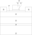
- FIG. 1 illustrates a structural view of a HEMT according to an embodiment of the present invention.
- FIG. 2 illustrates a structural view of a buffer layer of a HEMT according to an embodiment of the present invention.
- FIG. 3 illustrates a structural view of a buffer layer of a HEMT according to an embodiment of the present invention.
- FIG. 1 illustrates a structural view of a HEMT according to an embodiment of the present invention.
- a substrate 12 such as a substrate made from silicon, silicon carbide, or aluminum oxide (or also referred to as sapphire) is provided, in which the substrate 12 could be a single-layered substrate, a multi-layered substrate, gradient substrate, or combination thereof.
- the substrate 12 could also include a silicon-on-insulator (SOI) substrate.
- SOI silicon-on-insulator
- the nucleation layer 14 preferably includes aluminum nitride (AlN) and the buffer layer 16 is preferably made of III-V semiconductors such as gallium nitride (GaN), in which a thickness of the buffer layer 16 could be between 0.5 microns to 10 microns.
- AlN aluminum nitride
- GaN gallium nitride
- the formation of the buffer layer 16 on the substrate 12 could be accomplished by a molecular-beam epitaxy (MBE) process, a metal organic chemical vapor deposition (MOCVD) process, a chemical vapor deposition (CVD) process, a hydride vapor phase epitaxy (HVPE) process, or combination thereof.
- MBE molecular-beam epitaxy
- MOCVD metal organic chemical vapor deposition
- CVD chemical vapor deposition
- HVPE hydride vapor phase epitaxy
- an unintentionally doped (UID) buffer layer 18 is formed on the surface of the buffer layer 16 .
- the UID buffer layer 18 is preferably made of III-V semiconductors such as gallium nitride (GaN) or more specifically unintentionally doped GaN.
- the formation of the UID buffer layer 18 on the buffer layer 16 could be accomplished by a molecular-beam epitaxy (MBE) process, a metal organic chemical vapor deposition (MOCVD) process, a chemical vapor deposition (CVD) process, a hydride vapor phase epitaxy (HVPE) process, or combination thereof.
- MBE molecular-beam epitaxy
- MOCVD metal organic chemical vapor deposition
- CVD chemical vapor deposition
- HVPE hydride vapor phase epitaxy
- the barrier layer 20 is preferably made of III-V semiconductor such as n-type or n-graded aluminum gallium nitride (Al x Ga 1-x N), in which 0 ⁇ x ⁇ 1, the barrier layer 20 preferably includes an epitaxial layer formed through epitaxial growth process, and the barrier layer 20 could include dopants such as silicon or germanium.
- III-V semiconductor such as n-type or n-graded aluminum gallium nitride (Al x Ga 1-x N)
- Al x Ga 1-x N aluminum gallium nitride
- the barrier layer 20 preferably includes an epitaxial layer formed through epitaxial growth process, and the barrier layer 20 could include dopants such as silicon or germanium.
- the formation of the barrier layer 20 on the UID buffer layer 18 could be accomplished by a molecular-beam epitaxy (MBE) process, a metal organic chemical vapor deposition (MOCVD) process, a chemical vapor deposition (CVD) process, a hydride vapor phase epitaxy (HVPE) process, or combination thereof.
- MBE molecular-beam epitaxy
- MOCVD metal organic chemical vapor deposition
- CVD chemical vapor deposition
- HVPE hydride vapor phase epitaxy
- a gate dielectric layer and a gate material layer are formed on the surface of the barrier layer 20 , and a photo-etching process is conducted to remove part of the gate material layer and part of the gate dielectric layer to form a gate structure 22 on the surface of the barrier layer 20 , in which the gate structure 22 preferably includes a patterned gate dielectric layer 24 and a gate electrode 26 .
- the bottom portion of the gate electrode 26 could include semiconductor material such as p-type GaN while the top portion of the gate electrode 26 could include metal such as Schottky metal including but not limited to for example gold (Au), silver (Ag), or platinum (Pt).
- the gate dielectric layer 24 could include silicon oxide, aluminum nitride (AlN), or aluminum oxide (AlO).
- a source electrode 28 and a drain electrode 30 are formed adjacent to two sides of the gate electrode 26 .
- the source electrode 28 and the drain electrode 30 are preferably made of metal.
- the source electrode 28 and the drain electrode 30 are preferably made of ohmic contact metals.
- each of the source electrode 28 and drain electrode 30 could include titanium (Ti), aluminum (Al), tungsten (W), palladium (Pd), or combination thereof.
- a photo-etching process to remove part of the barrier layer 20 adjacent to two sides of the gate electrode 26 for forming a recess, conduct an electroplating process, sputtering process, resistance heating evaporation process, electron beam evaporation process, physical vapor deposition (PVD) process, chemical vapor deposition (CVD) process, or combination thereof to form electrode materials in the recess, and then pattern the electrode materials through etching process to form the source electrode 28 and the drain electrode 30 .
- PVD physical vapor deposition
- CVD chemical vapor deposition
- FIG. 2 illustrates a structural view of the buffer layer 16 of a HEMT according to an embodiment of the present invention.
- the buffer layer 16 includes a first buffer layer 300 , a second buffer layer 400 , and a third buffer layer 500 , in which the first buffer layer 300 further includes a first layer 31 , a second layer 32 , a third layer 33 , a fourth layer 34 , a fifth layer 35 , a sixth layer 36 , a seventh layer 37 , an eighth layer 38 , a ninth layer 39 , and tenth layer 40 , the second buffer layer 400 includes a first layer 41 , a second layer 42 , a third layer 43 , a fourth layer 44 , a fifth layer 45 , a sixth layer 46 , a seventh layer 47 , an eighth layer 48 , a ninth layer 49 , and tenth layer 50 , and the third buffer layer 500 includes a first layer 51 , a second layer 52 , a third buffer layer 500 , in which the first buffer layer 300 further includes
- the odd number layers within the first buffer layer 300 preferably include Al y Ga 1-y N while the even number layers include Al x Ga 1-x N.
- the first layer 31 , the third layer 33 , the fifth layer 35 , the seventh layer 37 , and the ninth layer 39 preferably include Al y Ga 1-y N while the second layer 32 , the fourth layer 34 , the sixth layer 36 , the eighth layer 38 , and the tenth layer 40 include Al x Ga 1-x N.
- the odd number layers within the second buffer layer 400 preferably include Al w Ga 1-w N while the even number layers include Al z Ga 1-z N.
- the first layer 41 , the third layer 43 , the fifth layer 45 , the seventh layer 47 , and the ninth layer 49 preferably include Al w Ga 1-w N while the second layer 42 , the fourth layer 44 , the sixth layer 46 , the eighth layer 48 , and the tenth layer 50 include Al z Ga 1-z N.
- the odd number layers within the third buffer layer 500 preferably include Al q Ga 1-q N while the even number layers include Al p Ga 1-p N.
- the first layer 51 , the third layer 53 , the fifth layer 55 , the seventh layer 57 , and the ninth layer 59 preferably include Al q Ga 1-q N while the second layer 52 , the fourth layer 54 , the sixth layer 56 , the eighth layer 58 , and the tenth layer 60 include Al p Ga 1-p N.
- each of the odd number layers and the even number layers within the first buffer layer 300 , the second buffer layer 400 , and the third buffer layer 500 include different concentrations of aluminum.
- the aluminum concentration index x from the even number layers of the first buffer layer 300 is preferably greater than the aluminum concentration index z from the even number layers of the second buffer layer 400
- the aluminum concentration index z from the even number layers of the second buffer layer 400 is greater than the aluminum concentration index p from even number layers of the third buffer layer 500
- the aluminum concentration index p from even number layers of the third buffer layer 500 is greater than the aluminum concentration index y from odd number layers of the first buffer layer 300
- the aluminum concentration index y from odd number layers of the first buffer layer 300 is greater than the aluminum concentration index w from odd number layers of the second buffer layer 400
- the aluminum concentration index w from odd number layers of the second buffer layer 400 is greater than the aluminum concentration index q from odd number layers of the third buffer layer 500 , or overall x>z>p>y>w
- the aluminum concentration index of the odd number layers and the even number layers from the first buffer layer 300 , the second buffer layer 400 , and the third buffer layer 500 could be having the aforementioned relationship of x>z>p>y>w>q as each of the odd number layers and even number layers could also include same or different thicknesses.
- the thickness tx of each of the even number layers of the first buffer layer 300 could be equal to the thickness tz of each of the even number layers of the second buffer layer 400
- the thickness tz of each of the even number layers of the second buffer layer 400 could be equal to the thickness tp of each of the even number layers of the third buffer layer 500
- the thickness tp of each of the even number layers of the third buffer layer 500 could be less than the thickness ty of each of the odd number layers of the first buffer layer 300
- the thickness ty of each of the odd number layers of the first buffer layer 300 could be equal to the thickness tw of each of the odd number layers of the second buffer layer 400
- the thickness tw of each of the odd number layers of the second buffer layer 400 could be equal to the thickness tq of each of the odd number layers of the third buffer layer 500
- FIG. 3 illustrates a structural view of the buffer layer 16 of a HEMT according to an embodiment of the present invention.
- each of the odd number layers and even number layers of the first buffer layer 300 , the second buffer layer 400 , and the third buffer layer 500 could include different thicknesses according to a second embodiment of the present invention.
- the thickness tx of each of the even number layers of the first buffer layer 300 could be less than the thickness tz of each of the even number layers of the second buffer layer 400
- the thickness tz of each of the even number layers of the second buffer layer 400 could be less than the thickness tp of each of the even number layers of the third buffer layer 500
- the thickness tp of each of the even number layers of the third buffer layer 500 could be less than the thickness ty of each of the odd number layers of the first buffer layer 300
- the thickness ty of each of the odd number layers of the first buffer layer 300 could be less than the thickness tw of each of the odd number layers of the second buffer layer 400
- the thickness tw of each of the odd number layers of the second buffer layer 400 could be less than the thickness tq of each of the odd number layers of the third buffer layer 500 , or overall tx ⁇ tz ⁇ tp ⁇ ty ⁇ tw ⁇ tq.
- each of the odd number layers and even number layers could also be having same or different thickness depending on the demand of the product.
- each of the even number layers of the first buffer layer 300 could be having same thickness tx
- each of the even number layers of the second buffer layer 400 could be having same thickness tz
- each of the even number layers of the third buffer layer 500 could be having same thickness tp
- each of the odd number layers of the first buffer layer 300 could be having same thickness ty
- each of the odd number layers of the second buffer layer 400 could be having same thickness tw
- each of the odd number layers of the third buffer layer 500 could be having same thickness tq, in which tx ⁇ tz ⁇ tp ⁇ ty ⁇ tw ⁇ tq.
- the odd number layers and the even number layers from the first buffer layer 300 , the second buffer layer 400 , and the third buffer layer 500 could be having different thicknesses overall according to the aforementioned thickness relationship tx ⁇ tz ⁇ tp ⁇ ty ⁇ tw ⁇ tq while each of the odd number layers and even number layers are also having different thicknesses.
- each of the even number layers of the first buffer layer 300 could have different thicknesses tx, in which the thickness of the second layer 32 could be less than or greater than the thickness of the fourth layer 34 , the thickness of the fourth layer 34 could be less than or greater than the thickness of the sixth layer 36 , the thickness of the sixth layer 36 could be less than or greater than the thickness of the eighth layer 38 , the thickness of the eighth layer 38 could be less than or greater than the thickness of the tenth layer 40 , and the thickness tx of each of the second layer 32 , fourth layer 34 , sixth layer 36 , eighth layer 38 , and tenth layer 40 is preferably less than the thickness tz of each of the even number layers of the second buffer layer 400 .
- Each of the even number layers of the second buffer layer 400 could have different thicknesses tz, in which the thickness of the second layer 42 could be less than or greater than the thickness of the fourth layer 44 , the thickness of the fourth layer 44 could be less than or greater than the thickness of the sixth layer 46 , the thickness of the sixth layer 46 could be less than or greater than the thickness of the eighth layer 48 , the thickness of the eighth layer 48 could be less than or greater than the thickness of the tenth layer 50 , and the thickness tz of each of the second layer 42 , fourth layer 44 , sixth layer 46 , eighth layer 48 , and tenth layer 40 is preferably less than the thickness tp of each of the even number layers of the third buffer layer 500 .
- Each of the even number layers of the third buffer layer 500 could have different thicknesses tp, in which the thickness of the second layer 52 could be less than or greater than the thickness of the fourth layer 54 , the thickness of the fourth layer 54 could be less than or greater than the thickness of the sixth layer 56 , the thickness of the sixth layer 56 could be less than or greater than the thickness of the eighth layer 58 , the thickness of the eighth layer 58 could be less than or greater than the thickness of the tenth layer 60 , and the thickness tp of each of the second layer 52 , fourth layer 54 , sixth layer 56 , eighth layer 58 , and tenth layer 60 is preferably less than the thickness ty of each of the odd number layers of the first buffer layer 300 .
- Each of the odd number layers of the first buffer layer 300 could have different thicknesses ty, in which the thickness of the first layer 31 could be less than or greater than the thickness of the third layer 33 , the thickness of the third layer 33 could be less than or greater than the thickness of the fifth layer 35 , the thickness of the fifth layer 35 could be less than or greater than the thickness of the seventh layer 37 , the thickness of the seventh layer 37 could be less than or greater than the thickness of the ninth layer 39 , and the thickness ty of each of the first layer 31 , third layer 33 , fifth layer 35 , seventh layer 37 , and ninth layer 39 is preferably less than the thickness tw of each of the odd number layers of the second buffer layer 400 .
- Each of the odd number layers of the second buffer layer 400 could have different thicknesses tw, in which the thickness of the first layer 41 could be less than or greater than the thickness of the third layer 43 , the thickness of the third layer 43 could be less than or greater than the thickness of the fifth layer 45 , the thickness of the fifth layer 45 could be less than or greater than the thickness of the seventh layer 47 , the thickness of the seventh layer 47 could be less than or greater than the thickness of the ninth layer 49 , and the thickness tw of each of the first layer 41 , third layer 43 , fifth layer 45 , seventh layer 47 , and ninth layer 49 is preferably less than the thickness tq of each of the odd number layers of the third buffer layer 500 .
- Each of the odd number layers of the third buffer layer 500 could have different thicknesses tq, in which the thickness of the first layer 51 could be less than or greater than the thickness of the third layer 53 , the thickness of the third layer 53 could be less than or greater than the thickness of the fifth layer 55 , the thickness of the fifth layer 55 could be less than or greater than the thickness of the seventh layer 57 , and the thickness of the seventh layer 57 could be less than or greater than the thickness of the ninth layer 59 .
- each of the odd number layers and the even number layers from the first buffer layer 300 , the second buffer layer 400 , and the third buffer layer 500 having different thicknesses as disclosed in the second embodiment could also include same and/or different aluminum concentration index.
- the aluminum concentration index x of the even number layers of the first buffer layer 300 could be equal to the aluminum concentration index z of the even number layers of the second buffer layer 400
- the aluminum concentration index z of the even number layers of the second buffer layer 400 could be equal to the aluminum concentration index p of the even number layers of the third buffer layer 500
- the aluminum concentration index p of the even number layers of the third buffer layer 500 could be greater than the aluminum concentration index y of the odd number layers of the first buffer layer 300
- the aluminum concentration index y of the odd number layers of the first buffer layer 300 could be equal to the aluminum concentration index w of the odd number layers of the second buffer layer 400
- the aluminum concentration index w of the odd number layers of the second buffer layer 400 could be equal to the aluminum concentration index q of the odd number layers of the third buffer layer 500
- the number of the buffer layers and the number of each of the buffer layers could all be adjusted according to the demand of the product.
- first buffer layer 300 only includes a first layer 31 and a second layer 32
- second buffer layer 400 also only includes a first layer 41 and a second layer 42
- the first layer 31 of the first buffer layer 300 preferably contacts the nucleation layer 14 or the substrate 12 directly as the second layer 42 of the second buffer layer 400 contacts the UID buffer layer 18 directly, which is also within the scope of the present invention.
Abstract
Description
Claims (17)
Applications Claiming Priority (2)
| Application Number | Priority Date | Filing Date | Title |
|---|---|---|---|
| CN201911125485.6A CN112820773A (en) | 2019-11-18 | 2019-11-18 | High electron mobility transistor |
| CN201911125485.6 | 2019-11-18 |
Publications (2)
| Publication Number | Publication Date |
|---|---|
| US20210151591A1 US20210151591A1 (en) | 2021-05-20 |
| US11257939B2 true US11257939B2 (en) | 2022-02-22 |
Family
ID=75852244
Family Applications (1)
| Application Number | Title | Priority Date | Filing Date |
|---|---|---|---|
| US16/711,451 Active US11257939B2 (en) | 2019-11-18 | 2019-12-12 | High electron mobility transistor |
Country Status (2)
| Country | Link |
|---|---|
| US (1) | US11257939B2 (en) |
| CN (1) | CN112820773A (en) |
Families Citing this family (3)
| Publication number | Priority date | Publication date | Assignee | Title |
|---|---|---|---|---|
| US20220328425A1 (en) * | 2021-04-12 | 2022-10-13 | Innoscience (Suzhou) Technology Co., Ltd. | Semiconductor device and method for manufacturing the same |
| US20220328674A1 (en) * | 2021-04-12 | 2022-10-13 | Innoscience (Suzhou) Technology Co., Ltd. | Semiconductor device and method for manufacturing the same |
| CN117203775A (en) * | 2021-04-12 | 2023-12-08 | 英诺赛科(苏州)半导体有限公司 | Semiconductor device and method for manufacturing the same |
Citations (13)
| Publication number | Priority date | Publication date | Assignee | Title |
|---|---|---|---|---|
| US7112830B2 (en) | 2002-11-25 | 2006-09-26 | Apa Enterprises, Inc. | Super lattice modification of overlying transistor |
| US20110272665A1 (en) * | 2010-05-07 | 2011-11-10 | Rohm Co., Ltd. | Nitride semiconductor device |
| US20120161152A1 (en) * | 2010-02-16 | 2012-06-28 | Ngk Insulators, Ltd. | Epitaxial substrate and method for manufacturing epitaxial substrate |
| US20120168719A1 (en) * | 2009-07-17 | 2012-07-05 | Dowa Electronics Materials Co., Ltd. | Epitaxial substrate for electronic device, in which current flows in lateral direction and method of producing the same |
| US20120211763A1 (en) * | 2011-02-22 | 2012-08-23 | Covalent Materials Corporation | Nitride semiconductor substrate and method of manufacturing the same |
| US20120261716A1 (en) * | 2011-04-15 | 2012-10-18 | Sanken Electric Co., Ltd. | Semiconductor device |
| US20130200495A1 (en) * | 2012-02-03 | 2013-08-08 | Transphorm Inc. | Buffer layer structures suited for iii-nitride devices with foreign substrates |
| US20140374771A1 (en) * | 2012-03-16 | 2014-12-25 | Furukawa Electric Co., Ltd. | Semiconductor multi-layer substrate, semiconductor device, and method for manufacturing the same |
| US20150060765A1 (en) * | 2013-09-05 | 2015-03-05 | Fujitsu Limited | Semiconductor device |
| US20160118486A1 (en) * | 2013-05-31 | 2016-04-28 | Sanken Electric Co., Ltd. | Semiconductor device |
| US20190006501A1 (en) * | 2017-06-30 | 2019-01-03 | Epistar Corporation | Semiconductor device |
| US20210057561A1 (en) * | 2019-08-20 | 2021-02-25 | Vanguard International Semiconductor Corporation | High electron mobility transistor device and methods for forming the same |
| US20210057562A1 (en) * | 2019-08-20 | 2021-02-25 | Vanguard International Semiconductor Corporation | High electron mobility transistor device and methods for forming the same |
Family Cites Families (4)
| Publication number | Priority date | Publication date | Assignee | Title |
|---|---|---|---|---|
| JP4058595B2 (en) * | 2001-08-20 | 2008-03-12 | サンケン電気株式会社 | Semiconductor light emitting device and manufacturing method thereof |
| KR101358633B1 (en) * | 2009-11-04 | 2014-02-04 | 도와 일렉트로닉스 가부시키가이샤 | Epitaxially laminated iii-nitride substrate |
| JP5785103B2 (en) * | 2012-01-16 | 2015-09-24 | シャープ株式会社 | Epitaxial wafers for heterojunction field effect transistors. |
| TWI546959B (en) * | 2015-01-21 | 2016-08-21 | 國立交通大學 | High electron mobility transistor |
-
2019
- 2019-11-18 CN CN201911125485.6A patent/CN112820773A/en active Pending
- 2019-12-12 US US16/711,451 patent/US11257939B2/en active Active
Patent Citations (14)
| Publication number | Priority date | Publication date | Assignee | Title |
|---|---|---|---|---|
| US7112830B2 (en) | 2002-11-25 | 2006-09-26 | Apa Enterprises, Inc. | Super lattice modification of overlying transistor |
| US20120168719A1 (en) * | 2009-07-17 | 2012-07-05 | Dowa Electronics Materials Co., Ltd. | Epitaxial substrate for electronic device, in which current flows in lateral direction and method of producing the same |
| US20120161152A1 (en) * | 2010-02-16 | 2012-06-28 | Ngk Insulators, Ltd. | Epitaxial substrate and method for manufacturing epitaxial substrate |
| US20110272665A1 (en) * | 2010-05-07 | 2011-11-10 | Rohm Co., Ltd. | Nitride semiconductor device |
| US20120211763A1 (en) * | 2011-02-22 | 2012-08-23 | Covalent Materials Corporation | Nitride semiconductor substrate and method of manufacturing the same |
| US20120261716A1 (en) * | 2011-04-15 | 2012-10-18 | Sanken Electric Co., Ltd. | Semiconductor device |
| US20130200495A1 (en) * | 2012-02-03 | 2013-08-08 | Transphorm Inc. | Buffer layer structures suited for iii-nitride devices with foreign substrates |
| US9685323B2 (en) | 2012-02-03 | 2017-06-20 | Transphorm Inc. | Buffer layer structures suited for III-nitride devices with foreign substrates |
| US20140374771A1 (en) * | 2012-03-16 | 2014-12-25 | Furukawa Electric Co., Ltd. | Semiconductor multi-layer substrate, semiconductor device, and method for manufacturing the same |
| US20160118486A1 (en) * | 2013-05-31 | 2016-04-28 | Sanken Electric Co., Ltd. | Semiconductor device |
| US20150060765A1 (en) * | 2013-09-05 | 2015-03-05 | Fujitsu Limited | Semiconductor device |
| US20190006501A1 (en) * | 2017-06-30 | 2019-01-03 | Epistar Corporation | Semiconductor device |
| US20210057561A1 (en) * | 2019-08-20 | 2021-02-25 | Vanguard International Semiconductor Corporation | High electron mobility transistor device and methods for forming the same |
| US20210057562A1 (en) * | 2019-08-20 | 2021-02-25 | Vanguard International Semiconductor Corporation | High electron mobility transistor device and methods for forming the same |
Also Published As
| Publication number | Publication date |
|---|---|
| US20210151591A1 (en) | 2021-05-20 |
| CN112820773A (en) | 2021-05-18 |
Similar Documents
| Publication | Publication Date | Title |
|---|---|---|
| US11257939B2 (en) | High electron mobility transistor | |
| US11322600B2 (en) | High electron mobility transistor | |
| US11894441B2 (en) | High electron mobility transistor and method for fabricating the same | |
| US20230378314A1 (en) | High electron mobility transistor and method for fabricating the same | |
| US20230335614A1 (en) | High electron mobility transistor and method for fabricating the same | |
| US20230361207A1 (en) | High electron mobility transistor and method for fabricating the same | |
| US10714607B1 (en) | High electron mobility transistor | |
| US11843046B2 (en) | High electron mobility transistor (HEMT) | |
| US20230387280A1 (en) | High electron mobility transistor and method for fabricating the same | |
| US20230231044A1 (en) | High electron mobility transistor and method for fabricating the same | |
| US20240038844A1 (en) | High electron mobility transistor and method for fabricating the same | |
| US20240128353A1 (en) | High electron mobility transistor and method for fabricating the same | |
| US20240136423A1 (en) | High electron mobility transistor and method for fabricating the same | |
| US20240038871A1 (en) | High electron mobility transistor and method for fabricating the same | |
| US20230335629A1 (en) | High electron mobility transistor | |
| US20240113215A1 (en) | High electron mobility transistor and method for fabricating the same | |
| US20240071758A1 (en) | High electron mobility transistor and method for fabricating the same | |
| US20240072126A1 (en) | Method for fabricating high electron mobility transistor | |
| TW202406146A (en) | High electron mobility transistor and method for fabricating the same |
Legal Events
| Date | Code | Title | Description |
|---|---|---|---|
| AS | Assignment |
Owner name: UNITED MICROELECTRONICS CORP., TAIWAN Free format text: ASSIGNMENT OF ASSIGNORS INTEREST;ASSIGNORS:CHEN, YEN-HSING;HSU, YU-MING;WANG, YU-CHI;AND OTHERS;REEL/FRAME:051255/0622 Effective date: 20191210 |
|
| FEPP | Fee payment procedure |
Free format text: ENTITY STATUS SET TO UNDISCOUNTED (ORIGINAL EVENT CODE: BIG.); ENTITY STATUS OF PATENT OWNER: LARGE ENTITY |
|
| STPP | Information on status: patent application and granting procedure in general |
Free format text: NON FINAL ACTION MAILED |
|
| STPP | Information on status: patent application and granting procedure in general |
Free format text: RESPONSE TO NON-FINAL OFFICE ACTION ENTERED AND FORWARDED TO EXAMINER |
|
| STPP | Information on status: patent application and granting procedure in general |
Free format text: NOTICE OF ALLOWANCE MAILED -- APPLICATION RECEIVED IN OFFICE OF PUBLICATIONS |
|
| STPP | Information on status: patent application and granting procedure in general |
Free format text: PUBLICATIONS -- ISSUE FEE PAYMENT RECEIVED |
|
| STCF | Information on status: patent grant |
Free format text: PATENTED CASE |