US11257939B2 - High electron mobility transistor - Google Patents

High electron mobility transistor Download PDF

Info

Publication number
US11257939B2
US11257939B2 US16/711,451 US201916711451A US11257939B2 US 11257939 B2 US11257939 B2 US 11257939B2 US 201916711451 A US201916711451 A US 201916711451A US 11257939 B2 US11257939 B2 US 11257939B2
Authority
US
United States
Prior art keywords
layer
buffer layer
buffer
thickness
hemt
Prior art date
Legal status (The legal status is an assumption and is not a legal conclusion. Google has not performed a legal analysis and makes no representation as to the accuracy of the status listed.)
Active
Application number
US16/711,451
Other versions
US20210151591A1 (en
Inventor
Yen-Hsing Chen
Yu-Ming Hsu
Yu-Chi Wang
Tsung-Mu Yang
Yu-Ren Wang
Current Assignee (The listed assignees may be inaccurate. Google has not performed a legal analysis and makes no representation or warranty as to the accuracy of the list.)
United Microelectronics Corp
Original Assignee
United Microelectronics Corp
Priority date (The priority date is an assumption and is not a legal conclusion. Google has not performed a legal analysis and makes no representation as to the accuracy of the date listed.)
Filing date
Publication date
Application filed by United Microelectronics Corp filed Critical United Microelectronics Corp
Assigned to UNITED MICROELECTRONICS CORP. reassignment UNITED MICROELECTRONICS CORP. ASSIGNMENT OF ASSIGNORS INTEREST (SEE DOCUMENT FOR DETAILS). Assignors: CHEN, YEN-HSING, HSU, YU-MING, WANG, YU-CHI, WANG, YU-REN, YANG, TSUNG-MU
Publication of US20210151591A1 publication Critical patent/US20210151591A1/en
Application granted granted Critical
Publication of US11257939B2 publication Critical patent/US11257939B2/en
Active legal-status Critical Current
Anticipated expiration legal-status Critical

Links

Images

Classifications

    • HELECTRICITY
    • H10SEMICONDUCTOR DEVICES; ELECTRIC SOLID-STATE DEVICES NOT OTHERWISE PROVIDED FOR
    • H10DINORGANIC ELECTRIC SEMICONDUCTOR DEVICES
    • H10D30/00Field-effect transistors [FET]
    • H10D30/40FETs having zero-dimensional [0D], one-dimensional [1D] or two-dimensional [2D] charge carrier gas channels
    • H10D30/47FETs having zero-dimensional [0D], one-dimensional [1D] or two-dimensional [2D] charge carrier gas channels having 2D charge carrier gas channels, e.g. nanoribbon FETs or high electron mobility transistors [HEMT]
    • H10D30/471High electron mobility transistors [HEMT] or high hole mobility transistors [HHMT]
    • H10D30/473High electron mobility transistors [HEMT] or high hole mobility transistors [HHMT] having confinement of carriers by multiple heterojunctions, e.g. quantum well HEMT
    • H10D30/4732High electron mobility transistors [HEMT] or high hole mobility transistors [HHMT] having confinement of carriers by multiple heterojunctions, e.g. quantum well HEMT using Group III-V semiconductor material
    • H01L29/7783
    • HELECTRICITY
    • H10SEMICONDUCTOR DEVICES; ELECTRIC SOLID-STATE DEVICES NOT OTHERWISE PROVIDED FOR
    • H10DINORGANIC ELECTRIC SEMICONDUCTOR DEVICES
    • H10D30/00Field-effect transistors [FET]
    • H10D30/40FETs having zero-dimensional [0D], one-dimensional [1D] or two-dimensional [2D] charge carrier gas channels
    • H10D30/47FETs having zero-dimensional [0D], one-dimensional [1D] or two-dimensional [2D] charge carrier gas channels having 2D charge carrier gas channels, e.g. nanoribbon FETs or high electron mobility transistors [HEMT]
    • H10D30/471High electron mobility transistors [HEMT] or high hole mobility transistors [HHMT]
    • H10D30/475High electron mobility transistors [HEMT] or high hole mobility transistors [HHMT] having wider bandgap layer formed on top of lower bandgap active layer, e.g. undoped barrier HEMTs such as i-AlGaN/GaN HEMTs
    • H10D30/4755High electron mobility transistors [HEMT] or high hole mobility transistors [HHMT] having wider bandgap layer formed on top of lower bandgap active layer, e.g. undoped barrier HEMTs such as i-AlGaN/GaN HEMTs having wide bandgap charge-carrier supplying layers, e.g. modulation doped HEMTs such as n-AlGaAs/GaAs HEMTs
    • H01L29/2003
    • H01L29/205
    • H01L29/7782
    • HELECTRICITY
    • H10SEMICONDUCTOR DEVICES; ELECTRIC SOLID-STATE DEVICES NOT OTHERWISE PROVIDED FOR
    • H10DINORGANIC ELECTRIC SEMICONDUCTOR DEVICES
    • H10D30/00Field-effect transistors [FET]
    • H10D30/01Manufacture or treatment
    • H10D30/015Manufacture or treatment of FETs having heterojunction interface channels or heterojunction gate electrodes, e.g. HEMT
    • HELECTRICITY
    • H10SEMICONDUCTOR DEVICES; ELECTRIC SOLID-STATE DEVICES NOT OTHERWISE PROVIDED FOR
    • H10DINORGANIC ELECTRIC SEMICONDUCTOR DEVICES
    • H10D30/00Field-effect transistors [FET]
    • H10D30/40FETs having zero-dimensional [0D], one-dimensional [1D] or two-dimensional [2D] charge carrier gas channels
    • H10D30/47FETs having zero-dimensional [0D], one-dimensional [1D] or two-dimensional [2D] charge carrier gas channels having 2D charge carrier gas channels, e.g. nanoribbon FETs or high electron mobility transistors [HEMT]
    • H10D30/471High electron mobility transistors [HEMT] or high hole mobility transistors [HHMT]
    • H10D30/473High electron mobility transistors [HEMT] or high hole mobility transistors [HHMT] having confinement of carriers by multiple heterojunctions, e.g. quantum well HEMT
    • HELECTRICITY
    • H10SEMICONDUCTOR DEVICES; ELECTRIC SOLID-STATE DEVICES NOT OTHERWISE PROVIDED FOR
    • H10DINORGANIC ELECTRIC SEMICONDUCTOR DEVICES
    • H10D62/00Semiconductor bodies, or regions thereof, of devices having potential barriers
    • H10D62/10Shapes, relative sizes or dispositions of the regions of the semiconductor bodies; Shapes of the semiconductor bodies
    • H10D62/124Shapes, relative sizes or dispositions of the regions of semiconductor bodies or of junctions between the regions
    • HELECTRICITY
    • H10SEMICONDUCTOR DEVICES; ELECTRIC SOLID-STATE DEVICES NOT OTHERWISE PROVIDED FOR
    • H10DINORGANIC ELECTRIC SEMICONDUCTOR DEVICES
    • H10D62/00Semiconductor bodies, or regions thereof, of devices having potential barriers
    • H10D62/10Shapes, relative sizes or dispositions of the regions of the semiconductor bodies; Shapes of the semiconductor bodies
    • H10D62/17Semiconductor regions connected to electrodes not carrying current to be rectified, amplified or switched, e.g. channel regions
    • H10D62/351Substrate regions of field-effect devices
    • H10D62/357Substrate regions of field-effect devices of FETs
    • H10D62/364Substrate regions of field-effect devices of FETs of IGFETs
    • HELECTRICITY
    • H10SEMICONDUCTOR DEVICES; ELECTRIC SOLID-STATE DEVICES NOT OTHERWISE PROVIDED FOR
    • H10DINORGANIC ELECTRIC SEMICONDUCTOR DEVICES
    • H10D62/00Semiconductor bodies, or regions thereof, of devices having potential barriers
    • H10D62/80Semiconductor bodies, or regions thereof, of devices having potential barriers characterised by the materials
    • H10D62/82Heterojunctions
    • H10D62/824Heterojunctions comprising only Group III-V materials heterojunctions, e.g. GaN/AlGaN heterojunctions
    • HELECTRICITY
    • H10SEMICONDUCTOR DEVICES; ELECTRIC SOLID-STATE DEVICES NOT OTHERWISE PROVIDED FOR
    • H10DINORGANIC ELECTRIC SEMICONDUCTOR DEVICES
    • H10D62/00Semiconductor bodies, or regions thereof, of devices having potential barriers
    • H10D62/10Shapes, relative sizes or dispositions of the regions of the semiconductor bodies; Shapes of the semiconductor bodies
    • H10D62/17Semiconductor regions connected to electrodes not carrying current to be rectified, amplified or switched, e.g. channel regions
    • H10D62/343Gate regions of field-effect devices having PN junction gates
    • HELECTRICITY
    • H10SEMICONDUCTOR DEVICES; ELECTRIC SOLID-STATE DEVICES NOT OTHERWISE PROVIDED FOR
    • H10DINORGANIC ELECTRIC SEMICONDUCTOR DEVICES
    • H10D62/00Semiconductor bodies, or regions thereof, of devices having potential barriers
    • H10D62/80Semiconductor bodies, or regions thereof, of devices having potential barriers characterised by the materials
    • H10D62/85Semiconductor bodies, or regions thereof, of devices having potential barriers characterised by the materials being Group III-V materials, e.g. GaAs
    • H10D62/8503Nitride Group III-V materials, e.g. AlN or GaN

Definitions

  • the invention relates to a high electron mobility transistor (HEMT).
  • HEMT high electron mobility transistor
  • High electron mobility transistor (HEMT) fabricated from GaN-based materials have various advantages in electrical, mechanical, and chemical aspects of the field. For instance, advantages including wide band gap, high break down voltage, high electron mobility, high elastic modulus, high piezoelectric and piezoresistive coefficients, and chemical inertness. All of these advantages allow GaN-based materials to be used in numerous applications including high intensity light emitting diodes (LEDs), power switching devices, regulators, battery protectors, display panel drivers, and communication devices.
  • LEDs high intensity light emitting diodes
  • a high electron mobility transistor includes a buffer layer having a first buffer layer and a second buffer layer on a substrate.
  • the first buffer layer includes a first layer of the first buffer layer comprising Al y Ga 1-y N and a second layer of the first buffer layer on the first layer of the first buffer layer comprising Al x Ga 1-x N.
  • the second buffer layer includes a first layer of the second buffer layer on the first buffer layer comprising Al w Ga 1-w N; and a second layer of the second buffer layer on the first layer of the second buffer layer comprising Al z Ga 1-z N and x>z>y>w.
  • a high electron mobility transistor includes a buffer layer having a first buffer layer and a second buffer layer on a substrate.
  • the first buffer layer includes a first layer of the first buffer layer on the substrate comprising Al y Ga 1-y N and a second layer of the first buffer layer on the first layer of the first buffer layer comprising Al x Ga 1-x N.
  • the second buffer layer includes a first layer of the second buffer layer on the first buffer layer comprising Al w Ga 1-w N and a second layer of the second buffer layer on the first layer of the second buffer layer, in which the second layer of the second buffer layer comprises Al z Ga 1-z N and a thickness of the second layer of the first buffer layer is less than a thickness of the second layer of the second buffer layer.
  • FIG. 1 illustrates a structural view of a HEMT according to an embodiment of the present invention.
  • FIG. 2 illustrates a structural view of a buffer layer of a HEMT according to an embodiment of the present invention.
  • FIG. 3 illustrates a structural view of a buffer layer of a HEMT according to an embodiment of the present invention.
  • FIG. 1 illustrates a structural view of a HEMT according to an embodiment of the present invention.
  • a substrate 12 such as a substrate made from silicon, silicon carbide, or aluminum oxide (or also referred to as sapphire) is provided, in which the substrate 12 could be a single-layered substrate, a multi-layered substrate, gradient substrate, or combination thereof.
  • the substrate 12 could also include a silicon-on-insulator (SOI) substrate.
  • SOI silicon-on-insulator
  • the nucleation layer 14 preferably includes aluminum nitride (AlN) and the buffer layer 16 is preferably made of III-V semiconductors such as gallium nitride (GaN), in which a thickness of the buffer layer 16 could be between 0.5 microns to 10 microns.
  • AlN aluminum nitride
  • GaN gallium nitride
  • the formation of the buffer layer 16 on the substrate 12 could be accomplished by a molecular-beam epitaxy (MBE) process, a metal organic chemical vapor deposition (MOCVD) process, a chemical vapor deposition (CVD) process, a hydride vapor phase epitaxy (HVPE) process, or combination thereof.
  • MBE molecular-beam epitaxy
  • MOCVD metal organic chemical vapor deposition
  • CVD chemical vapor deposition
  • HVPE hydride vapor phase epitaxy
  • an unintentionally doped (UID) buffer layer 18 is formed on the surface of the buffer layer 16 .
  • the UID buffer layer 18 is preferably made of III-V semiconductors such as gallium nitride (GaN) or more specifically unintentionally doped GaN.
  • the formation of the UID buffer layer 18 on the buffer layer 16 could be accomplished by a molecular-beam epitaxy (MBE) process, a metal organic chemical vapor deposition (MOCVD) process, a chemical vapor deposition (CVD) process, a hydride vapor phase epitaxy (HVPE) process, or combination thereof.
  • MBE molecular-beam epitaxy
  • MOCVD metal organic chemical vapor deposition
  • CVD chemical vapor deposition
  • HVPE hydride vapor phase epitaxy
  • the barrier layer 20 is preferably made of III-V semiconductor such as n-type or n-graded aluminum gallium nitride (Al x Ga 1-x N), in which 0 ⁇ x ⁇ 1, the barrier layer 20 preferably includes an epitaxial layer formed through epitaxial growth process, and the barrier layer 20 could include dopants such as silicon or germanium.
  • III-V semiconductor such as n-type or n-graded aluminum gallium nitride (Al x Ga 1-x N)
  • Al x Ga 1-x N aluminum gallium nitride
  • the barrier layer 20 preferably includes an epitaxial layer formed through epitaxial growth process, and the barrier layer 20 could include dopants such as silicon or germanium.
  • the formation of the barrier layer 20 on the UID buffer layer 18 could be accomplished by a molecular-beam epitaxy (MBE) process, a metal organic chemical vapor deposition (MOCVD) process, a chemical vapor deposition (CVD) process, a hydride vapor phase epitaxy (HVPE) process, or combination thereof.
  • MBE molecular-beam epitaxy
  • MOCVD metal organic chemical vapor deposition
  • CVD chemical vapor deposition
  • HVPE hydride vapor phase epitaxy
  • a gate dielectric layer and a gate material layer are formed on the surface of the barrier layer 20 , and a photo-etching process is conducted to remove part of the gate material layer and part of the gate dielectric layer to form a gate structure 22 on the surface of the barrier layer 20 , in which the gate structure 22 preferably includes a patterned gate dielectric layer 24 and a gate electrode 26 .
  • the bottom portion of the gate electrode 26 could include semiconductor material such as p-type GaN while the top portion of the gate electrode 26 could include metal such as Schottky metal including but not limited to for example gold (Au), silver (Ag), or platinum (Pt).
  • the gate dielectric layer 24 could include silicon oxide, aluminum nitride (AlN), or aluminum oxide (AlO).
  • a source electrode 28 and a drain electrode 30 are formed adjacent to two sides of the gate electrode 26 .
  • the source electrode 28 and the drain electrode 30 are preferably made of metal.
  • the source electrode 28 and the drain electrode 30 are preferably made of ohmic contact metals.
  • each of the source electrode 28 and drain electrode 30 could include titanium (Ti), aluminum (Al), tungsten (W), palladium (Pd), or combination thereof.
  • a photo-etching process to remove part of the barrier layer 20 adjacent to two sides of the gate electrode 26 for forming a recess, conduct an electroplating process, sputtering process, resistance heating evaporation process, electron beam evaporation process, physical vapor deposition (PVD) process, chemical vapor deposition (CVD) process, or combination thereof to form electrode materials in the recess, and then pattern the electrode materials through etching process to form the source electrode 28 and the drain electrode 30 .
  • PVD physical vapor deposition
  • CVD chemical vapor deposition
  • FIG. 2 illustrates a structural view of the buffer layer 16 of a HEMT according to an embodiment of the present invention.
  • the buffer layer 16 includes a first buffer layer 300 , a second buffer layer 400 , and a third buffer layer 500 , in which the first buffer layer 300 further includes a first layer 31 , a second layer 32 , a third layer 33 , a fourth layer 34 , a fifth layer 35 , a sixth layer 36 , a seventh layer 37 , an eighth layer 38 , a ninth layer 39 , and tenth layer 40 , the second buffer layer 400 includes a first layer 41 , a second layer 42 , a third layer 43 , a fourth layer 44 , a fifth layer 45 , a sixth layer 46 , a seventh layer 47 , an eighth layer 48 , a ninth layer 49 , and tenth layer 50 , and the third buffer layer 500 includes a first layer 51 , a second layer 52 , a third buffer layer 500 , in which the first buffer layer 300 further includes
  • the odd number layers within the first buffer layer 300 preferably include Al y Ga 1-y N while the even number layers include Al x Ga 1-x N.
  • the first layer 31 , the third layer 33 , the fifth layer 35 , the seventh layer 37 , and the ninth layer 39 preferably include Al y Ga 1-y N while the second layer 32 , the fourth layer 34 , the sixth layer 36 , the eighth layer 38 , and the tenth layer 40 include Al x Ga 1-x N.
  • the odd number layers within the second buffer layer 400 preferably include Al w Ga 1-w N while the even number layers include Al z Ga 1-z N.
  • the first layer 41 , the third layer 43 , the fifth layer 45 , the seventh layer 47 , and the ninth layer 49 preferably include Al w Ga 1-w N while the second layer 42 , the fourth layer 44 , the sixth layer 46 , the eighth layer 48 , and the tenth layer 50 include Al z Ga 1-z N.
  • the odd number layers within the third buffer layer 500 preferably include Al q Ga 1-q N while the even number layers include Al p Ga 1-p N.
  • the first layer 51 , the third layer 53 , the fifth layer 55 , the seventh layer 57 , and the ninth layer 59 preferably include Al q Ga 1-q N while the second layer 52 , the fourth layer 54 , the sixth layer 56 , the eighth layer 58 , and the tenth layer 60 include Al p Ga 1-p N.
  • each of the odd number layers and the even number layers within the first buffer layer 300 , the second buffer layer 400 , and the third buffer layer 500 include different concentrations of aluminum.
  • the aluminum concentration index x from the even number layers of the first buffer layer 300 is preferably greater than the aluminum concentration index z from the even number layers of the second buffer layer 400
  • the aluminum concentration index z from the even number layers of the second buffer layer 400 is greater than the aluminum concentration index p from even number layers of the third buffer layer 500
  • the aluminum concentration index p from even number layers of the third buffer layer 500 is greater than the aluminum concentration index y from odd number layers of the first buffer layer 300
  • the aluminum concentration index y from odd number layers of the first buffer layer 300 is greater than the aluminum concentration index w from odd number layers of the second buffer layer 400
  • the aluminum concentration index w from odd number layers of the second buffer layer 400 is greater than the aluminum concentration index q from odd number layers of the third buffer layer 500 , or overall x>z>p>y>w
  • the aluminum concentration index of the odd number layers and the even number layers from the first buffer layer 300 , the second buffer layer 400 , and the third buffer layer 500 could be having the aforementioned relationship of x>z>p>y>w>q as each of the odd number layers and even number layers could also include same or different thicknesses.
  • the thickness tx of each of the even number layers of the first buffer layer 300 could be equal to the thickness tz of each of the even number layers of the second buffer layer 400
  • the thickness tz of each of the even number layers of the second buffer layer 400 could be equal to the thickness tp of each of the even number layers of the third buffer layer 500
  • the thickness tp of each of the even number layers of the third buffer layer 500 could be less than the thickness ty of each of the odd number layers of the first buffer layer 300
  • the thickness ty of each of the odd number layers of the first buffer layer 300 could be equal to the thickness tw of each of the odd number layers of the second buffer layer 400
  • the thickness tw of each of the odd number layers of the second buffer layer 400 could be equal to the thickness tq of each of the odd number layers of the third buffer layer 500
  • FIG. 3 illustrates a structural view of the buffer layer 16 of a HEMT according to an embodiment of the present invention.
  • each of the odd number layers and even number layers of the first buffer layer 300 , the second buffer layer 400 , and the third buffer layer 500 could include different thicknesses according to a second embodiment of the present invention.
  • the thickness tx of each of the even number layers of the first buffer layer 300 could be less than the thickness tz of each of the even number layers of the second buffer layer 400
  • the thickness tz of each of the even number layers of the second buffer layer 400 could be less than the thickness tp of each of the even number layers of the third buffer layer 500
  • the thickness tp of each of the even number layers of the third buffer layer 500 could be less than the thickness ty of each of the odd number layers of the first buffer layer 300
  • the thickness ty of each of the odd number layers of the first buffer layer 300 could be less than the thickness tw of each of the odd number layers of the second buffer layer 400
  • the thickness tw of each of the odd number layers of the second buffer layer 400 could be less than the thickness tq of each of the odd number layers of the third buffer layer 500 , or overall tx ⁇ tz ⁇ tp ⁇ ty ⁇ tw ⁇ tq.
  • each of the odd number layers and even number layers could also be having same or different thickness depending on the demand of the product.
  • each of the even number layers of the first buffer layer 300 could be having same thickness tx
  • each of the even number layers of the second buffer layer 400 could be having same thickness tz
  • each of the even number layers of the third buffer layer 500 could be having same thickness tp
  • each of the odd number layers of the first buffer layer 300 could be having same thickness ty
  • each of the odd number layers of the second buffer layer 400 could be having same thickness tw
  • each of the odd number layers of the third buffer layer 500 could be having same thickness tq, in which tx ⁇ tz ⁇ tp ⁇ ty ⁇ tw ⁇ tq.
  • the odd number layers and the even number layers from the first buffer layer 300 , the second buffer layer 400 , and the third buffer layer 500 could be having different thicknesses overall according to the aforementioned thickness relationship tx ⁇ tz ⁇ tp ⁇ ty ⁇ tw ⁇ tq while each of the odd number layers and even number layers are also having different thicknesses.
  • each of the even number layers of the first buffer layer 300 could have different thicknesses tx, in which the thickness of the second layer 32 could be less than or greater than the thickness of the fourth layer 34 , the thickness of the fourth layer 34 could be less than or greater than the thickness of the sixth layer 36 , the thickness of the sixth layer 36 could be less than or greater than the thickness of the eighth layer 38 , the thickness of the eighth layer 38 could be less than or greater than the thickness of the tenth layer 40 , and the thickness tx of each of the second layer 32 , fourth layer 34 , sixth layer 36 , eighth layer 38 , and tenth layer 40 is preferably less than the thickness tz of each of the even number layers of the second buffer layer 400 .
  • Each of the even number layers of the second buffer layer 400 could have different thicknesses tz, in which the thickness of the second layer 42 could be less than or greater than the thickness of the fourth layer 44 , the thickness of the fourth layer 44 could be less than or greater than the thickness of the sixth layer 46 , the thickness of the sixth layer 46 could be less than or greater than the thickness of the eighth layer 48 , the thickness of the eighth layer 48 could be less than or greater than the thickness of the tenth layer 50 , and the thickness tz of each of the second layer 42 , fourth layer 44 , sixth layer 46 , eighth layer 48 , and tenth layer 40 is preferably less than the thickness tp of each of the even number layers of the third buffer layer 500 .
  • Each of the even number layers of the third buffer layer 500 could have different thicknesses tp, in which the thickness of the second layer 52 could be less than or greater than the thickness of the fourth layer 54 , the thickness of the fourth layer 54 could be less than or greater than the thickness of the sixth layer 56 , the thickness of the sixth layer 56 could be less than or greater than the thickness of the eighth layer 58 , the thickness of the eighth layer 58 could be less than or greater than the thickness of the tenth layer 60 , and the thickness tp of each of the second layer 52 , fourth layer 54 , sixth layer 56 , eighth layer 58 , and tenth layer 60 is preferably less than the thickness ty of each of the odd number layers of the first buffer layer 300 .
  • Each of the odd number layers of the first buffer layer 300 could have different thicknesses ty, in which the thickness of the first layer 31 could be less than or greater than the thickness of the third layer 33 , the thickness of the third layer 33 could be less than or greater than the thickness of the fifth layer 35 , the thickness of the fifth layer 35 could be less than or greater than the thickness of the seventh layer 37 , the thickness of the seventh layer 37 could be less than or greater than the thickness of the ninth layer 39 , and the thickness ty of each of the first layer 31 , third layer 33 , fifth layer 35 , seventh layer 37 , and ninth layer 39 is preferably less than the thickness tw of each of the odd number layers of the second buffer layer 400 .
  • Each of the odd number layers of the second buffer layer 400 could have different thicknesses tw, in which the thickness of the first layer 41 could be less than or greater than the thickness of the third layer 43 , the thickness of the third layer 43 could be less than or greater than the thickness of the fifth layer 45 , the thickness of the fifth layer 45 could be less than or greater than the thickness of the seventh layer 47 , the thickness of the seventh layer 47 could be less than or greater than the thickness of the ninth layer 49 , and the thickness tw of each of the first layer 41 , third layer 43 , fifth layer 45 , seventh layer 47 , and ninth layer 49 is preferably less than the thickness tq of each of the odd number layers of the third buffer layer 500 .
  • Each of the odd number layers of the third buffer layer 500 could have different thicknesses tq, in which the thickness of the first layer 51 could be less than or greater than the thickness of the third layer 53 , the thickness of the third layer 53 could be less than or greater than the thickness of the fifth layer 55 , the thickness of the fifth layer 55 could be less than or greater than the thickness of the seventh layer 57 , and the thickness of the seventh layer 57 could be less than or greater than the thickness of the ninth layer 59 .
  • each of the odd number layers and the even number layers from the first buffer layer 300 , the second buffer layer 400 , and the third buffer layer 500 having different thicknesses as disclosed in the second embodiment could also include same and/or different aluminum concentration index.
  • the aluminum concentration index x of the even number layers of the first buffer layer 300 could be equal to the aluminum concentration index z of the even number layers of the second buffer layer 400
  • the aluminum concentration index z of the even number layers of the second buffer layer 400 could be equal to the aluminum concentration index p of the even number layers of the third buffer layer 500
  • the aluminum concentration index p of the even number layers of the third buffer layer 500 could be greater than the aluminum concentration index y of the odd number layers of the first buffer layer 300
  • the aluminum concentration index y of the odd number layers of the first buffer layer 300 could be equal to the aluminum concentration index w of the odd number layers of the second buffer layer 400
  • the aluminum concentration index w of the odd number layers of the second buffer layer 400 could be equal to the aluminum concentration index q of the odd number layers of the third buffer layer 500
  • the number of the buffer layers and the number of each of the buffer layers could all be adjusted according to the demand of the product.
  • first buffer layer 300 only includes a first layer 31 and a second layer 32
  • second buffer layer 400 also only includes a first layer 41 and a second layer 42
  • the first layer 31 of the first buffer layer 300 preferably contacts the nucleation layer 14 or the substrate 12 directly as the second layer 42 of the second buffer layer 400 contacts the UID buffer layer 18 directly, which is also within the scope of the present invention.

Landscapes

  • Junction Field-Effect Transistors (AREA)
  • Chemical & Material Sciences (AREA)
  • Engineering & Computer Science (AREA)
  • Materials Engineering (AREA)

Abstract

A high electron mobility transistor (HEMT) includes a buffer layer on a substrate, in which the buffer layer includes a first buffer layer and a second buffer layer. Preferably, the first buffer layer includes a first layer of the first buffer layer comprising AlyGa1-yN on the substrate and a second layer of the first buffer layer comprising AlxGa1-xN on the first layer of the first buffer layer. The second buffer layer includes a first layer of the second buffer layer comprising AlwGa1-wN on the first buffer layer and a second layer of the second buffer layer comprising AlzGa1-zN on the first layer of the second buffer layer, in which x>z>y>w.

Description

BACKGROUND OF THE INVENTION 1. Field of the Invention
The invention relates to a high electron mobility transistor (HEMT).
2. Description of the Prior Art
High electron mobility transistor (HEMT) fabricated from GaN-based materials have various advantages in electrical, mechanical, and chemical aspects of the field. For instance, advantages including wide band gap, high break down voltage, high electron mobility, high elastic modulus, high piezoelectric and piezoresistive coefficients, and chemical inertness. All of these advantages allow GaN-based materials to be used in numerous applications including high intensity light emitting diodes (LEDs), power switching devices, regulators, battery protectors, display panel drivers, and communication devices.
SUMMARY OF THE INVENTION
According to an embodiment of the present invention, a high electron mobility transistor (HEMT) includes a buffer layer having a first buffer layer and a second buffer layer on a substrate. Preferably, the first buffer layer includes a first layer of the first buffer layer comprising AlyGa1-yN and a second layer of the first buffer layer on the first layer of the first buffer layer comprising AlxGa1-xN. The second buffer layer includes a first layer of the second buffer layer on the first buffer layer comprising AlwGa1-wN; and a second layer of the second buffer layer on the first layer of the second buffer layer comprising AlzGa1-zN and x>z>y>w.
According to another aspect of the present invention, a high electron mobility transistor (HEMT) includes a buffer layer having a first buffer layer and a second buffer layer on a substrate. Preferably, the first buffer layer includes a first layer of the first buffer layer on the substrate comprising AlyGa1-yN and a second layer of the first buffer layer on the first layer of the first buffer layer comprising AlxGa1-xN. The second buffer layer includes a first layer of the second buffer layer on the first buffer layer comprising AlwGa1-wN and a second layer of the second buffer layer on the first layer of the second buffer layer, in which the second layer of the second buffer layer comprises AlzGa1-zN and a thickness of the second layer of the first buffer layer is less than a thickness of the second layer of the second buffer layer.
These and other objectives of the present invention will no doubt become obvious to those of ordinary skill in the art after reading the following detailed description of the preferred embodiment that is illustrated in the various figures and drawings.
BRIEF DESCRIPTION OF THE DRAWINGS
FIG. 1 illustrates a structural view of a HEMT according to an embodiment of the present invention.
FIG. 2 illustrates a structural view of a buffer layer of a HEMT according to an embodiment of the present invention.
FIG. 3 illustrates a structural view of a buffer layer of a HEMT according to an embodiment of the present invention.
DETAILED DESCRIPTION
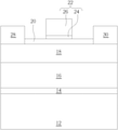
Referring to FIG. 1, FIG. 1 illustrates a structural view of a HEMT according to an embodiment of the present invention. As shown in FIG. 1, a substrate 12 such as a substrate made from silicon, silicon carbide, or aluminum oxide (or also referred to as sapphire) is provided, in which the substrate 12 could be a single-layered substrate, a multi-layered substrate, gradient substrate, or combination thereof. According to other embodiment of the present invention, the substrate 12 could also include a silicon-on-insulator (SOI) substrate.
Next, a selective nucleation layer 14 and a buffer layer 16 are formed on the substrate 12. According to an embodiment of the present invention, the nucleation layer 14 preferably includes aluminum nitride (AlN) and the buffer layer 16 is preferably made of III-V semiconductors such as gallium nitride (GaN), in which a thickness of the buffer layer 16 could be between 0.5 microns to 10 microns. According to an embodiment of the present invention, the formation of the buffer layer 16 on the substrate 12 could be accomplished by a molecular-beam epitaxy (MBE) process, a metal organic chemical vapor deposition (MOCVD) process, a chemical vapor deposition (CVD) process, a hydride vapor phase epitaxy (HVPE) process, or combination thereof.
Next, an unintentionally doped (UID) buffer layer 18 is formed on the surface of the buffer layer 16. In this embodiment, the UID buffer layer 18 is preferably made of III-V semiconductors such as gallium nitride (GaN) or more specifically unintentionally doped GaN. According to an embodiment of the present invention, the formation of the UID buffer layer 18 on the buffer layer 16 could be accomplished by a molecular-beam epitaxy (MBE) process, a metal organic chemical vapor deposition (MOCVD) process, a chemical vapor deposition (CVD) process, a hydride vapor phase epitaxy (HVPE) process, or combination thereof.
Next, a barrier layer 20 is formed on the surface of the UID buffer layer 18. In this embodiment, the barrier layer 20 is preferably made of III-V semiconductor such as n-type or n-graded aluminum gallium nitride (AlxGa1-xN), in which 0<x<1, the barrier layer 20 preferably includes an epitaxial layer formed through epitaxial growth process, and the barrier layer 20 could include dopants such as silicon or germanium. Similar to the buffer layer 16 and the UID buffer layer 18, the formation of the barrier layer 20 on the UID buffer layer 18 could be accomplished by a molecular-beam epitaxy (MBE) process, a metal organic chemical vapor deposition (MOCVD) process, a chemical vapor deposition (CVD) process, a hydride vapor phase epitaxy (HVPE) process, or combination thereof.
Next, a gate dielectric layer and a gate material layer are formed on the surface of the barrier layer 20, and a photo-etching process is conducted to remove part of the gate material layer and part of the gate dielectric layer to form a gate structure 22 on the surface of the barrier layer 20, in which the gate structure 22 preferably includes a patterned gate dielectric layer 24 and a gate electrode 26. In this embodiment, the bottom portion of the gate electrode 26 could include semiconductor material such as p-type GaN while the top portion of the gate electrode 26 could include metal such as Schottky metal including but not limited to for example gold (Au), silver (Ag), or platinum (Pt). The gate dielectric layer 24 could include silicon oxide, aluminum nitride (AlN), or aluminum oxide (AlO).
Next, a source electrode 28 and a drain electrode 30 are formed adjacent to two sides of the gate electrode 26. In this embodiment, the source electrode 28 and the drain electrode 30 are preferably made of metal. Nevertheless, in contrast to the top portion of the gate electrode 26 made of Schottky metal, the source electrode 28 and the drain electrode 30 are preferably made of ohmic contact metals. According to an embodiment of the present invention, each of the source electrode 28 and drain electrode 30 could include titanium (Ti), aluminum (Al), tungsten (W), palladium (Pd), or combination thereof. Moreover, it would be desirable to first conduct a photo-etching process to remove part of the barrier layer 20 adjacent to two sides of the gate electrode 26 for forming a recess, conduct an electroplating process, sputtering process, resistance heating evaporation process, electron beam evaporation process, physical vapor deposition (PVD) process, chemical vapor deposition (CVD) process, or combination thereof to form electrode materials in the recess, and then pattern the electrode materials through etching process to form the source electrode 28 and the drain electrode 30.
Referring again to FIG. 2, FIG. 2 illustrates a structural view of the buffer layer 16 of a HEMT according to an embodiment of the present invention. As shown in FIG. 2, the buffer layer 16 includes a first buffer layer 300, a second buffer layer 400, and a third buffer layer 500, in which the first buffer layer 300 further includes a first layer 31, a second layer 32, a third layer 33, a fourth layer 34, a fifth layer 35, a sixth layer 36, a seventh layer 37, an eighth layer 38, a ninth layer 39, and tenth layer 40, the second buffer layer 400 includes a first layer 41, a second layer 42, a third layer 43, a fourth layer 44, a fifth layer 45, a sixth layer 46, a seventh layer 47, an eighth layer 48, a ninth layer 49, and tenth layer 50, and the third buffer layer 500 includes a first layer 51, a second layer 52, a third layer 53, a fourth layer 54, a fifth layer 55, a sixth layer 56, a seventh layer 57, an eighth layer 58, a ninth layer 59, and tenth layer 60.
In this embodiment, the odd number layers within the first buffer layer 300 preferably include AlyGa1-yN while the even number layers include AlxGa1-xN. For instance, the first layer 31, the third layer 33, the fifth layer 35, the seventh layer 37, and the ninth layer 39 preferably include AlyGa1-yN while the second layer 32, the fourth layer 34, the sixth layer 36, the eighth layer 38, and the tenth layer 40 include AlxGa1-xN. The odd number layers within the second buffer layer 400 preferably include AlwGa1-wN while the even number layers include AlzGa1-zN. For instance, the first layer 41, the third layer 43, the fifth layer 45, the seventh layer 47, and the ninth layer 49 preferably include AlwGa1-wN while the second layer 42, the fourth layer 44, the sixth layer 46, the eighth layer 48, and the tenth layer 50 include AlzGa1-zN. The odd number layers within the third buffer layer 500 preferably include AlqGa1-qN while the even number layers include AlpGa1-pN. For instance, the first layer 51, the third layer 53, the fifth layer 55, the seventh layer 57, and the ninth layer 59 preferably include AlqGa1-qN while the second layer 52, the fourth layer 54, the sixth layer 56, the eighth layer 58, and the tenth layer 60 include AlpGa1-pN.
According to a first embodiment of the present invention, each of the odd number layers and the even number layers within the first buffer layer 300, the second buffer layer 400, and the third buffer layer 500 include different concentrations of aluminum. For instance, the aluminum concentration index x from the even number layers of the first buffer layer 300 is preferably greater than the aluminum concentration index z from the even number layers of the second buffer layer 400, the aluminum concentration index z from the even number layers of the second buffer layer 400 is greater than the aluminum concentration index p from even number layers of the third buffer layer 500, the aluminum concentration index p from even number layers of the third buffer layer 500 is greater than the aluminum concentration index y from odd number layers of the first buffer layer 300, the aluminum concentration index y from odd number layers of the first buffer layer 300 is greater than the aluminum concentration index w from odd number layers of the second buffer layer 400, the aluminum concentration index w from odd number layers of the second buffer layer 400 is greater than the aluminum concentration index q from odd number layers of the third buffer layer 500, or overall x>z>p>y>w>q.
Moreover in the first embodiment of the present invention, the aluminum concentration index of the odd number layers and the even number layers from the first buffer layer 300, the second buffer layer 400, and the third buffer layer 500 could be having the aforementioned relationship of x>z>p>y>w>q as each of the odd number layers and even number layers could also include same or different thicknesses. For instance, the thickness tx of each of the even number layers of the first buffer layer 300 could be equal to the thickness tz of each of the even number layers of the second buffer layer 400, the thickness tz of each of the even number layers of the second buffer layer 400 could be equal to the thickness tp of each of the even number layers of the third buffer layer 500, the thickness tp of each of the even number layers of the third buffer layer 500 could be less than the thickness ty of each of the odd number layers of the first buffer layer 300, the thickness ty of each of the odd number layers of the first buffer layer 300 could be equal to the thickness tw of each of the odd number layers of the second buffer layer 400, the thickness tw of each of the odd number layers of the second buffer layer 400 could be equal to the thickness tq of each of the odd number layers of the third buffer layer 500, or overall tx=tz=tp<ty=tw=tq.
Referring to FIG. 3, FIG. 3 illustrates a structural view of the buffer layer 16 of a HEMT according to an embodiment of the present invention. As shown in FIG. 3, each of the odd number layers and even number layers of the first buffer layer 300, the second buffer layer 400, and the third buffer layer 500 could include different thicknesses according to a second embodiment of the present invention. For instance, the thickness tx of each of the even number layers of the first buffer layer 300 could be less than the thickness tz of each of the even number layers of the second buffer layer 400, the thickness tz of each of the even number layers of the second buffer layer 400 could be less than the thickness tp of each of the even number layers of the third buffer layer 500, the thickness tp of each of the even number layers of the third buffer layer 500 could be less than the thickness ty of each of the odd number layers of the first buffer layer 300, the thickness ty of each of the odd number layers of the first buffer layer 300 could be less than the thickness tw of each of the odd number layers of the second buffer layer 400, the thickness tw of each of the odd number layers of the second buffer layer 400 could be less than the thickness tq of each of the odd number layers of the third buffer layer 500, or overall tx<tz<tp<ty<tw<tq.
It should be noted that in additional to the odd number layers and the even number layers from the first buffer layer 300, the second buffer layer 400, and the third buffer layer 500 having different thicknesses overall as disclosed previously, each of the odd number layers and even number layers could also be having same or different thickness depending on the demand of the product. For instance, each of the even number layers of the first buffer layer 300 could be having same thickness tx, each of the even number layers of the second buffer layer 400 could be having same thickness tz, each of the even number layers of the third buffer layer 500 could be having same thickness tp, each of the odd number layers of the first buffer layer 300 could be having same thickness ty, each of the odd number layers of the second buffer layer 400 could be having same thickness tw, and each of the odd number layers of the third buffer layer 500 could be having same thickness tq, in which tx<tz<tp<ty<tw<tq.
Alternatively, instead of having the odd number layers and the even number layers from the first buffer layer 300, the second buffer layer 400, and the third buffer layer 500 having different thicknesses overall while each of the odd number layers having same thickness and each of the even number layers having same thickness, the odd number layers and the even number layers from the first buffer layer 300, the second buffer layer 400, and the third buffer layer 500 could be having different thicknesses overall according to the aforementioned thickness relationship tx<tz<tp<ty<tw<tq while each of the odd number layers and even number layers are also having different thicknesses. For instance, each of the even number layers of the first buffer layer 300 could have different thicknesses tx, in which the thickness of the second layer 32 could be less than or greater than the thickness of the fourth layer 34, the thickness of the fourth layer 34 could be less than or greater than the thickness of the sixth layer 36, the thickness of the sixth layer 36 could be less than or greater than the thickness of the eighth layer 38, the thickness of the eighth layer 38 could be less than or greater than the thickness of the tenth layer 40, and the thickness tx of each of the second layer 32, fourth layer 34, sixth layer 36, eighth layer 38, and tenth layer 40 is preferably less than the thickness tz of each of the even number layers of the second buffer layer 400.
Each of the even number layers of the second buffer layer 400 could have different thicknesses tz, in which the thickness of the second layer 42 could be less than or greater than the thickness of the fourth layer 44, the thickness of the fourth layer 44 could be less than or greater than the thickness of the sixth layer 46, the thickness of the sixth layer 46 could be less than or greater than the thickness of the eighth layer 48, the thickness of the eighth layer 48 could be less than or greater than the thickness of the tenth layer 50, and the thickness tz of each of the second layer 42, fourth layer 44, sixth layer 46, eighth layer 48, and tenth layer 40 is preferably less than the thickness tp of each of the even number layers of the third buffer layer 500.
Each of the even number layers of the third buffer layer 500 could have different thicknesses tp, in which the thickness of the second layer 52 could be less than or greater than the thickness of the fourth layer 54, the thickness of the fourth layer 54 could be less than or greater than the thickness of the sixth layer 56, the thickness of the sixth layer 56 could be less than or greater than the thickness of the eighth layer 58, the thickness of the eighth layer 58 could be less than or greater than the thickness of the tenth layer 60, and the thickness tp of each of the second layer 52, fourth layer 54, sixth layer 56, eighth layer 58, and tenth layer 60 is preferably less than the thickness ty of each of the odd number layers of the first buffer layer 300.
Each of the odd number layers of the first buffer layer 300 could have different thicknesses ty, in which the thickness of the first layer 31 could be less than or greater than the thickness of the third layer 33, the thickness of the third layer 33 could be less than or greater than the thickness of the fifth layer 35, the thickness of the fifth layer 35 could be less than or greater than the thickness of the seventh layer 37, the thickness of the seventh layer 37 could be less than or greater than the thickness of the ninth layer 39, and the thickness ty of each of the first layer 31, third layer 33, fifth layer 35, seventh layer 37, and ninth layer 39 is preferably less than the thickness tw of each of the odd number layers of the second buffer layer 400.
Each of the odd number layers of the second buffer layer 400 could have different thicknesses tw, in which the thickness of the first layer 41 could be less than or greater than the thickness of the third layer 43, the thickness of the third layer 43 could be less than or greater than the thickness of the fifth layer 45, the thickness of the fifth layer 45 could be less than or greater than the thickness of the seventh layer 47, the thickness of the seventh layer 47 could be less than or greater than the thickness of the ninth layer 49, and the thickness tw of each of the first layer 41, third layer 43, fifth layer 45, seventh layer 47, and ninth layer 49 is preferably less than the thickness tq of each of the odd number layers of the third buffer layer 500.
Each of the odd number layers of the third buffer layer 500 could have different thicknesses tq, in which the thickness of the first layer 51 could be less than or greater than the thickness of the third layer 53, the thickness of the third layer 53 could be less than or greater than the thickness of the fifth layer 55, the thickness of the fifth layer 55 could be less than or greater than the thickness of the seventh layer 57, and the thickness of the seventh layer 57 could be less than or greater than the thickness of the ninth layer 59.
In addition to each of the odd number layers and the even number layers from the first buffer layer 300, the second buffer layer 400, and the third buffer layer 500 having different thicknesses as disclosed in the second embodiment, each of the odd number layers and even number layers could also include same and/or different aluminum concentration index. For instance, the aluminum concentration index x of the even number layers of the first buffer layer 300 could be equal to the aluminum concentration index z of the even number layers of the second buffer layer 400, the aluminum concentration index z of the even number layers of the second buffer layer 400 could be equal to the aluminum concentration index p of the even number layers of the third buffer layer 500, the aluminum concentration index p of the even number layers of the third buffer layer 500 could be greater than the aluminum concentration index y of the odd number layers of the first buffer layer 300, the aluminum concentration index y of the odd number layers of the first buffer layer 300 could be equal to the aluminum concentration index w of the odd number layers of the second buffer layer 400, the aluminum concentration index w of the odd number layers of the second buffer layer 400 could be equal to the aluminum concentration index q of the odd number layers of the third buffer layer 500, or overall x=z=p>y=w=q.
It should be noted that even though three buffer layers including the first buffer layer 300, the second buffer layer 400, and the third buffer layer 500 and buffer layers preferably made of five layers of AlyGa1-yN, five layers of AlxGa1-xN, five layers of AlwGa1-wN, five layers of AlzGa1-z N, five layers of AlqGa1-qN, and five layers of AlpGa1-pN are disclosed in the aforementioned embodiments, the number of the buffer layers and the number of each of the buffer layers could all be adjusted according to the demand of the product. For instance, it would be desirable to only form two buffer layers such as a first buffer layer 300 and a second buffer layer 400 on the substrate 12, in which the first buffer layer 300 only includes a first layer 31 and a second layer 32, the second buffer layer 400 also only includes a first layer 41 and a second layer 42, and the first layer 31 of the first buffer layer 300 preferably contacts the nucleation layer 14 or the substrate 12 directly as the second layer 42 of the second buffer layer 400 contacts the UID buffer layer 18 directly, which is also within the scope of the present invention. By following the aforementioned approach to repeatedly stack buffer layers having different aluminum concentrations and/or different thicknesses, it would be desirable to relieve strain resides within the buffer layers thereby improving the overall performance of the HEMT.
Those skilled in the art will readily observe that numerous modifications and alterations of the device and method may be made while retaining the teachings of the invention. Accordingly, the above disclosure should be construed as limited only by the metes and bounds of the appended claims.

Claims (17)

What is claimed is:
1. A high electron mobility transistor (HEMT), comprising:
a nucleation layer on a substrate;
a buffer layer on the nucleation layer, wherein the buffer layer comprises:
a first buffer layer comprising:
a first layer of the first buffer layer on and directly contacting a top surface of the nucleation layer, wherein the first layer of the first buffer layer comprises AlyGa1-yN;
a second layer of the first buffer layer on and directly contacting a top surface of the first layer of the first buffer layer, wherein the second layer of the first buffer layer comprises AlxGa1-xN;
a second buffer layer comprising:
a first layer of the second buffer layer on the first buffer layer, wherein the first layer of the second buffer layer comprises AlwGa1-wN; and
a second layer of the second buffer layer on a top surface of the first layer of the second buffer layer, wherein the second layer of the second buffer layer comprises AlzGa1-zN and x>z>y>w;
a third buffer layer comprising:
a first layer of the third buffer layer on the second buffer layer, wherein the first layer of the third buffer layer comprises AlqGa1-qN; and
a second layer of the third buffer layer on the first layer of the third buffer layer, wherein the second layer of the third buffer layer comprises AlpGa1-pN and x>z>p>y>w>q.
2. The HEMT of claim 1, wherein the first buffer layer comprises:
a third layer of the first buffer layer on the second layer of the first buffer layer, wherein the third layer of the first buffer layer comprises AlyGa1-yN; and
a fourth layer of the first buffer layer on the third layer of the first buffer layer, wherein the fourth layer of the first buffer layer comprises AlxGa1-xN.
3. The HEMT of claim 1, wherein the second buffer layer comprises:
a third layer of the second buffer layer on the second layer of the second buffer layer, wherein the third layer of the second buffer layer comprises AlwGa1-wN; and
a fourth layer of the second buffer layer on the third layer of the second buffer layer, wherein the fourth layer of the second buffer layer comprises AlzGa1-zN.
4. The HEMT of claim 1, wherein the third buffer layer comprises:
a third layer of the third buffer layer on the second layer of the third buffer layer, wherein the third layer of the third buffer layer comprises AlqGa1-qN; and
a fourth layer of the third buffer layer on the third layer of the third buffer layer, wherein the fourth layer of the third buffer layer comprises AlpGa1-pN.
5. The HEMT of claim 1, wherein a thickness of the first layer of the first buffer layer is equal to a thickness of the first layer of the second buffer layer.
6. The HEMT of claim 1, wherein a thickness of the second layer of the first buffer layer is equal to a thickness of the second layer of the second buffer layer.
7. The HEMT of claim 1, wherein a thickness of the second layer of the first buffer layer is less than a thickness of the first layer of the first buffer layer.
8. The HEMT of claim 1, wherein a thickness of the second layer of the second buffer layer is less than a thickness of the first layer of the second buffer layer.
9. The HEMT of claim 1, further comprising:
an unintentionally doped (UID) buffer layer on the buffer layer;
a barrier layer on the UID buffer layer;
a gate electrode on the barrier layer; and
a source electrode and a drain electrode adjacent to two sides of the gate electrode.
10. A high electron mobility transistor (HEMT), comprising:
a nucleation layer on a substrate;
a buffer layer on the nucleation layer, wherein the buffer layer comprises:
a first buffer layer comprising:
a first layer of the first buffer layer on and directly contacting a top surface of the nucleation layer, wherein the first layer of the first buffer layer comprises AlyGa1-yN;
a second layer of the first buffer layer on a top surface of the first layer of the first buffer layer, wherein the second layer of the first buffer layer comprises AlxGa1-xN;
a second buffer layer comprising:
a first layer of the second buffer layer on and directly contacting the first buffer layer, wherein the first layer of the second buffer layer comprises AlwGa1-wN and the first layer of the second buffer layer is made of a single material; and
a second layer of the second buffer layer on a top surface of the first layer of the second buffer layer, wherein the second layer of the second buffer layer comprises AlzGa1-zN, the second layer of the second buffer layer is made of a single material, a total thickness of the second layer of the first buffer layer is less than a total thickness of the second layer of the second buffer layer, and a total thickness of the first layer of the first buffer layer is less than a total thickness of the first layer of the second buffer layer;
a third buffer layer comprising:
a first layer of the third buffer layer on the second buffer layer, wherein the first layer of the third buffer layer comprises AlqGa1-qN; and
a second layer of the third buffer layer on the first layer of the third buffer layer, wherein the second layer of the third buffer layer comprises AlpGa1-pN and x=z=p>y=w=q.
11. The HEMT of claim 10, wherein the first buffer layer comprises:
a third layer of the first buffer layer on the second layer of the first buffer layer, wherein the third layer of the first buffer layer comprises AlyGa1-yN; and
a fourth layer of the first buffer layer on the third layer of the first buffer layer, wherein the fourth layer of the first buffer layer comprises AlxGa1-xN.
12. The HEMT of claim 10, wherein the second buffer layer comprises:
a third layer of the second buffer layer on the second layer of the second buffer layer, wherein the third layer of the second buffer layer comprises AlwGa1-wN; and
a fourth layer of the second buffer layer on the third layer of the second buffer layer, wherein the fourth layer of the second buffer layer comprises AlzGa1-zN.
13. The HEMT of claim 10, wherein the third buffer layer comprises:
a third layer of the third buffer layer on the second layer of the third buffer layer, wherein the third layer of the third buffer layer comprises AlqGa1-qN; and
a fourth layer of the third buffer layer on the third layer of the third buffer layer, wherein the fourth layer of the third buffer layer comprises AlpGa1-pN.
14. The HEMT of claim 10, wherein a thickness of the second layer of the second buffer layer is less than a thickness of the second layer of the third buffer layer.
15. The HEMT of claim 10, wherein a thickness of the second layer of the third buffer layer is less than a thickness of the first layer of the first buffer layer.
16. The HEMT of claim 10, wherein a thickness of the first layer of the second buffer layer is less than a thickness of the first layer of the third buffer layer.
17. The HEMT of claim 10, further comprising:
an unintentionally doped (UID) buffer layer on the buffer layer;
a barrier layer on the UID buffer layer;
a gate electrode on the barrier layer; and
a source electrode and a drain electrode adjacent to two sides of the gate electrode.
US16/711,451 2019-11-18 2019-12-12 High electron mobility transistor Active US11257939B2 (en)

Applications Claiming Priority (2)

Application Number Priority Date Filing Date Title
CN201911125485.6 2019-11-18
CN201911125485.6A CN112820773B (en) 2019-11-18 2019-11-18 A high electron mobility transistor

Publications (2)

Publication Number Publication Date
US20210151591A1 US20210151591A1 (en) 2021-05-20
US11257939B2 true US11257939B2 (en) 2022-02-22

Family

ID=75852244

Family Applications (1)

Application Number Title Priority Date Filing Date
US16/711,451 Active US11257939B2 (en) 2019-11-18 2019-12-12 High electron mobility transistor

Country Status (2)

Country Link
US (1) US11257939B2 (en)
CN (1) CN112820773B (en)

Cited By (1)

* Cited by examiner, † Cited by third party
Publication number Priority date Publication date Assignee Title
US20240379765A1 (en) * 2023-05-10 2024-11-14 Gan Systems Inc. Superlattice epitaxial structure with varying lattice parameter differences

Families Citing this family (8)

* Cited by examiner, † Cited by third party
Publication number Priority date Publication date Assignee Title
WO2022217413A1 (en) * 2021-04-12 2022-10-20 Innoscience (Suzhou) Technology Co., Ltd. Semiconductor device and method for manufacturing thereof
US12125801B2 (en) * 2021-04-12 2024-10-22 Innoscience (Suzhou) Technology Co., Ltd. Semiconductor device and method for manufacturing the same
US12274082B2 (en) 2021-04-12 2025-04-08 Innoscience (Suzhou) Technology Co., Ltd. Semiconductor device and method for manufacturing the same
US12125902B2 (en) * 2021-04-12 2024-10-22 Innoscience (Suzhou) Technology Co., Ltd. Semiconductor device and method for manufacturing the same
CN116964752A (en) * 2021-04-12 2023-10-27 英诺赛科(苏州)半导体有限公司 Semiconductor device and manufacturing method thereof
US12289901B2 (en) 2021-04-12 2025-04-29 Innoscience (Suzhou) Technology Co., Ltd. Semiconductor device and method for manufacturing the same
US12279444B2 (en) 2021-04-12 2025-04-15 Innoscience (Suzhou) Technology Co., Ltd. Semiconductor device and method for manufacturing the same
US12317532B2 (en) * 2021-04-12 2025-05-27 Innoscience (Suzhou) Technology Co., Ltd. Semiconductor device and method for manufacturing the same

Citations (13)

* Cited by examiner, † Cited by third party
Publication number Priority date Publication date Assignee Title
US7112830B2 (en) 2002-11-25 2006-09-26 Apa Enterprises, Inc. Super lattice modification of overlying transistor
US20110272665A1 (en) * 2010-05-07 2011-11-10 Rohm Co., Ltd. Nitride semiconductor device
US20120161152A1 (en) * 2010-02-16 2012-06-28 Ngk Insulators, Ltd. Epitaxial substrate and method for manufacturing epitaxial substrate
US20120168719A1 (en) * 2009-07-17 2012-07-05 Dowa Electronics Materials Co., Ltd. Epitaxial substrate for electronic device, in which current flows in lateral direction and method of producing the same
US20120211763A1 (en) * 2011-02-22 2012-08-23 Covalent Materials Corporation Nitride semiconductor substrate and method of manufacturing the same
US20120261716A1 (en) * 2011-04-15 2012-10-18 Sanken Electric Co., Ltd. Semiconductor device
US20130200495A1 (en) * 2012-02-03 2013-08-08 Transphorm Inc. Buffer layer structures suited for iii-nitride devices with foreign substrates
US20140374771A1 (en) * 2012-03-16 2014-12-25 Furukawa Electric Co., Ltd. Semiconductor multi-layer substrate, semiconductor device, and method for manufacturing the same
US20150060765A1 (en) * 2013-09-05 2015-03-05 Fujitsu Limited Semiconductor device
US20160118486A1 (en) * 2013-05-31 2016-04-28 Sanken Electric Co., Ltd. Semiconductor device
US20190006501A1 (en) * 2017-06-30 2019-01-03 Epistar Corporation Semiconductor device
US20210057561A1 (en) * 2019-08-20 2021-02-25 Vanguard International Semiconductor Corporation High electron mobility transistor device and methods for forming the same
US20210057562A1 (en) * 2019-08-20 2021-02-25 Vanguard International Semiconductor Corporation High electron mobility transistor device and methods for forming the same

Family Cites Families (4)

* Cited by examiner, † Cited by third party
Publication number Priority date Publication date Assignee Title
JP4058595B2 (en) * 2001-08-20 2008-03-12 サンケン電気株式会社 Semiconductor light emitting device and manufacturing method thereof
EP2498282A4 (en) * 2009-11-04 2014-06-25 Dowa Electronics Materials Co Ltd NITRIDE III SUBSTRATE WITH EPITAXIAL STRATIFICATION
JP5785103B2 (en) * 2012-01-16 2015-09-24 シャープ株式会社 Epitaxial wafers for heterojunction field effect transistors.
TWI546959B (en) * 2015-01-21 2016-08-21 國立交通大學 High speed transistor

Patent Citations (14)

* Cited by examiner, † Cited by third party
Publication number Priority date Publication date Assignee Title
US7112830B2 (en) 2002-11-25 2006-09-26 Apa Enterprises, Inc. Super lattice modification of overlying transistor
US20120168719A1 (en) * 2009-07-17 2012-07-05 Dowa Electronics Materials Co., Ltd. Epitaxial substrate for electronic device, in which current flows in lateral direction and method of producing the same
US20120161152A1 (en) * 2010-02-16 2012-06-28 Ngk Insulators, Ltd. Epitaxial substrate and method for manufacturing epitaxial substrate
US20110272665A1 (en) * 2010-05-07 2011-11-10 Rohm Co., Ltd. Nitride semiconductor device
US20120211763A1 (en) * 2011-02-22 2012-08-23 Covalent Materials Corporation Nitride semiconductor substrate and method of manufacturing the same
US20120261716A1 (en) * 2011-04-15 2012-10-18 Sanken Electric Co., Ltd. Semiconductor device
US20130200495A1 (en) * 2012-02-03 2013-08-08 Transphorm Inc. Buffer layer structures suited for iii-nitride devices with foreign substrates
US9685323B2 (en) 2012-02-03 2017-06-20 Transphorm Inc. Buffer layer structures suited for III-nitride devices with foreign substrates
US20140374771A1 (en) * 2012-03-16 2014-12-25 Furukawa Electric Co., Ltd. Semiconductor multi-layer substrate, semiconductor device, and method for manufacturing the same
US20160118486A1 (en) * 2013-05-31 2016-04-28 Sanken Electric Co., Ltd. Semiconductor device
US20150060765A1 (en) * 2013-09-05 2015-03-05 Fujitsu Limited Semiconductor device
US20190006501A1 (en) * 2017-06-30 2019-01-03 Epistar Corporation Semiconductor device
US20210057561A1 (en) * 2019-08-20 2021-02-25 Vanguard International Semiconductor Corporation High electron mobility transistor device and methods for forming the same
US20210057562A1 (en) * 2019-08-20 2021-02-25 Vanguard International Semiconductor Corporation High electron mobility transistor device and methods for forming the same

Cited By (1)

* Cited by examiner, † Cited by third party
Publication number Priority date Publication date Assignee Title
US20240379765A1 (en) * 2023-05-10 2024-11-14 Gan Systems Inc. Superlattice epitaxial structure with varying lattice parameter differences

Also Published As

Publication number Publication date
CN112820773A (en) 2021-05-18
CN112820773B (en) 2024-05-07
US20210151591A1 (en) 2021-05-20

Similar Documents

Publication Publication Date Title
US11257939B2 (en) High electron mobility transistor
US20230378314A1 (en) High electron mobility transistor and method for fabricating the same
US12328889B2 (en) High electron mobility transistor and method for fabricating the same
US11894441B2 (en) High electron mobility transistor and method for fabricating the same
US12107157B2 (en) High electron mobility transistor and method for fabricating the same
US10714607B1 (en) High electron mobility transistor
US11843046B2 (en) High electron mobility transistor (HEMT)
US20250380441A1 (en) High electron mobility transistor and method for fabricating the same
US20240387720A1 (en) High electron mobility transistor and method for fabricating the same
US12369371B2 (en) High electron mobility transistor and method for fabricating the same
US12336245B2 (en) High electron mobility transistor and method for fabricating the same
US12310045B2 (en) High electron mobility transistor
US20240113215A1 (en) High electron mobility transistor and method for fabricating the same

Legal Events

Date Code Title Description
AS Assignment

Owner name: UNITED MICROELECTRONICS CORP., TAIWAN

Free format text: ASSIGNMENT OF ASSIGNORS INTEREST;ASSIGNORS:CHEN, YEN-HSING;HSU, YU-MING;WANG, YU-CHI;AND OTHERS;REEL/FRAME:051255/0622

Effective date: 20191210

FEPP Fee payment procedure

Free format text: ENTITY STATUS SET TO UNDISCOUNTED (ORIGINAL EVENT CODE: BIG.); ENTITY STATUS OF PATENT OWNER: LARGE ENTITY

STPP Information on status: patent application and granting procedure in general

Free format text: NON FINAL ACTION MAILED

STPP Information on status: patent application and granting procedure in general

Free format text: RESPONSE TO NON-FINAL OFFICE ACTION ENTERED AND FORWARDED TO EXAMINER

STPP Information on status: patent application and granting procedure in general

Free format text: NOTICE OF ALLOWANCE MAILED -- APPLICATION RECEIVED IN OFFICE OF PUBLICATIONS

STPP Information on status: patent application and granting procedure in general

Free format text: PUBLICATIONS -- ISSUE FEE PAYMENT RECEIVED

STCF Information on status: patent grant

Free format text: PATENTED CASE

MAFP Maintenance fee payment

Free format text: PAYMENT OF MAINTENANCE FEE, 4TH YEAR, LARGE ENTITY (ORIGINAL EVENT CODE: M1551); ENTITY STATUS OF PATENT OWNER: LARGE ENTITY

Year of fee payment: 4