US11245364B2 - Amplifying device and amplifying system comprising the same - Google Patents
Amplifying device and amplifying system comprising the same Download PDFInfo
- Publication number
- US11245364B2 US11245364B2 US16/817,811 US202016817811A US11245364B2 US 11245364 B2 US11245364 B2 US 11245364B2 US 202016817811 A US202016817811 A US 202016817811A US 11245364 B2 US11245364 B2 US 11245364B2
- Authority
- US
- United States
- Prior art keywords
- amplifying
- packaged
- amplifier
- units
- amplifiers
- Prior art date
- Legal status (The legal status is an assumption and is not a legal conclusion. Google has not performed a legal analysis and makes no representation as to the accuracy of the status listed.)
- Active, expires
Links
Images


Classifications
-
- H—ELECTRICITY
- H04—ELECTRIC COMMUNICATION TECHNIQUE
- H04B—TRANSMISSION
- H04B1/00—Details of transmission systems, not covered by a single one of groups H04B3/00 - H04B13/00; Details of transmission systems not characterised by the medium used for transmission
- H04B1/02—Transmitters
- H04B1/04—Circuits
-
- H10W44/20—
-
- H—ELECTRICITY
- H03—ELECTRONIC CIRCUITRY
- H03F—AMPLIFIERS
- H03F1/00—Details of amplifiers with only discharge tubes, only semiconductor devices or only unspecified devices as amplifying elements
- H03F1/02—Modifications of amplifiers to raise the efficiency, e.g. gliding Class A stages, use of an auxiliary oscillation
- H03F1/0205—Modifications of amplifiers to raise the efficiency, e.g. gliding Class A stages, use of an auxiliary oscillation in transistor amplifiers
- H03F1/0288—Modifications of amplifiers to raise the efficiency, e.g. gliding Class A stages, use of an auxiliary oscillation in transistor amplifiers using a main and one or several auxiliary peaking amplifiers whereby the load is connected to the main amplifier using an impedance inverter, e.g. Doherty amplifiers
-
- H—ELECTRICITY
- H03—ELECTRONIC CIRCUITRY
- H03F—AMPLIFIERS
- H03F1/00—Details of amplifiers with only discharge tubes, only semiconductor devices or only unspecified devices as amplifying elements
- H03F1/02—Modifications of amplifiers to raise the efficiency, e.g. gliding Class A stages, use of an auxiliary oscillation
- H03F1/0205—Modifications of amplifiers to raise the efficiency, e.g. gliding Class A stages, use of an auxiliary oscillation in transistor amplifiers
- H03F1/0294—Modifications of amplifiers to raise the efficiency, e.g. gliding Class A stages, use of an auxiliary oscillation in transistor amplifiers using vector summing of two or more constant amplitude phase-modulated signals
-
- H—ELECTRICITY
- H03—ELECTRONIC CIRCUITRY
- H03F—AMPLIFIERS
- H03F1/00—Details of amplifiers with only discharge tubes, only semiconductor devices or only unspecified devices as amplifying elements
- H03F1/56—Modifications of input or output impedances, not otherwise provided for
- H03F1/565—Modifications of input or output impedances, not otherwise provided for using inductive elements
-
- H—ELECTRICITY
- H03—ELECTRONIC CIRCUITRY
- H03F—AMPLIFIERS
- H03F3/00—Amplifiers with only discharge tubes or only semiconductor devices as amplifying elements
- H03F3/189—High-frequency amplifiers, e.g. radio frequency amplifiers
- H03F3/19—High-frequency amplifiers, e.g. radio frequency amplifiers with semiconductor devices only
- H03F3/193—High-frequency amplifiers, e.g. radio frequency amplifiers with semiconductor devices only with field-effect devices
-
- H—ELECTRICITY
- H03—ELECTRONIC CIRCUITRY
- H03F—AMPLIFIERS
- H03F3/00—Amplifiers with only discharge tubes or only semiconductor devices as amplifying elements
- H03F3/189—High-frequency amplifiers, e.g. radio frequency amplifiers
- H03F3/19—High-frequency amplifiers, e.g. radio frequency amplifiers with semiconductor devices only
- H03F3/195—High-frequency amplifiers, e.g. radio frequency amplifiers with semiconductor devices only in integrated circuits
-
- H—ELECTRICITY
- H03—ELECTRONIC CIRCUITRY
- H03F—AMPLIFIERS
- H03F3/00—Amplifiers with only discharge tubes or only semiconductor devices as amplifying elements
- H03F3/20—Power amplifiers, e.g. Class B amplifiers, Class C amplifiers
- H03F3/21—Power amplifiers, e.g. Class B amplifiers, Class C amplifiers with semiconductor devices only
- H03F3/211—Power amplifiers, e.g. Class B amplifiers, Class C amplifiers with semiconductor devices only using a combination of several amplifiers
-
- H—ELECTRICITY
- H03—ELECTRONIC CIRCUITRY
- H03F—AMPLIFIERS
- H03F3/00—Amplifiers with only discharge tubes or only semiconductor devices as amplifying elements
- H03F3/20—Power amplifiers, e.g. Class B amplifiers, Class C amplifiers
- H03F3/21—Power amplifiers, e.g. Class B amplifiers, Class C amplifiers with semiconductor devices only
- H03F3/217—Class D power amplifiers; Switching amplifiers
- H03F3/2176—Class E amplifiers
-
- H—ELECTRICITY
- H03—ELECTRONIC CIRCUITRY
- H03F—AMPLIFIERS
- H03F3/00—Amplifiers with only discharge tubes or only semiconductor devices as amplifying elements
- H03F3/20—Power amplifiers, e.g. Class B amplifiers, Class C amplifiers
- H03F3/21—Power amplifiers, e.g. Class B amplifiers, Class C amplifiers with semiconductor devices only
- H03F3/217—Class D power amplifiers; Switching amplifiers
- H03F3/2178—Class D power amplifiers; Switching amplifiers using more than one switch or switching amplifier in parallel or in series
-
- H—ELECTRICITY
- H03—ELECTRONIC CIRCUITRY
- H03F—AMPLIFIERS
- H03F3/00—Amplifiers with only discharge tubes or only semiconductor devices as amplifying elements
- H03F3/20—Power amplifiers, e.g. Class B amplifiers, Class C amplifiers
- H03F3/24—Power amplifiers, e.g. Class B amplifiers, Class C amplifiers of transmitter output stages
- H03F3/245—Power amplifiers, e.g. Class B amplifiers, Class C amplifiers of transmitter output stages with semiconductor devices only
-
- H—ELECTRICITY
- H04—ELECTRIC COMMUNICATION TECHNIQUE
- H04B—TRANSMISSION
- H04B1/00—Details of transmission systems, not covered by a single one of groups H04B3/00 - H04B13/00; Details of transmission systems not characterised by the medium used for transmission
- H04B1/02—Transmitters
- H04B1/04—Circuits
- H04B1/0458—Arrangements for matching and coupling between power amplifier and antenna or between amplifying stages
-
- H—ELECTRICITY
- H03—ELECTRONIC CIRCUITRY
- H03F—AMPLIFIERS
- H03F2200/00—Indexing scheme relating to amplifiers
- H03F2200/222—A circuit being added at the input of an amplifier to adapt the input impedance of the amplifier
-
- H—ELECTRICITY
- H03—ELECTRONIC CIRCUITRY
- H03F—AMPLIFIERS
- H03F2200/00—Indexing scheme relating to amplifiers
- H03F2200/387—A circuit being added at the output of an amplifier to adapt the output impedance of the amplifier
-
- H—ELECTRICITY
- H03—ELECTRONIC CIRCUITRY
- H03F—AMPLIFIERS
- H03F2200/00—Indexing scheme relating to amplifiers
- H03F2200/423—Amplifier output adaptation especially for transmission line coupling purposes, e.g. impedance adaptation
-
- H—ELECTRICITY
- H03—ELECTRONIC CIRCUITRY
- H03F—AMPLIFIERS
- H03F2200/00—Indexing scheme relating to amplifiers
- H03F2200/451—Indexing scheme relating to amplifiers the amplifier being a radio frequency amplifier
-
- H—ELECTRICITY
- H04—ELECTRIC COMMUNICATION TECHNIQUE
- H04B—TRANSMISSION
- H04B1/00—Details of transmission systems, not covered by a single one of groups H04B3/00 - H04B13/00; Details of transmission systems not characterised by the medium used for transmission
- H04B1/02—Transmitters
- H04B1/04—Circuits
- H04B2001/0408—Circuits with power amplifiers
- H04B2001/0416—Circuits with power amplifiers having gain or transmission power control
-
- H—ELECTRICITY
- H04—ELECTRIC COMMUNICATION TECHNIQUE
- H04B—TRANSMISSION
- H04B1/00—Details of transmission systems, not covered by a single one of groups H04B3/00 - H04B13/00; Details of transmission systems not characterised by the medium used for transmission
- H04B1/02—Transmitters
- H04B1/04—Circuits
- H04B2001/0408—Circuits with power amplifiers
- H04B2001/045—Circuits with power amplifiers with means for improving efficiency
-
- H10W44/206—
-
- H10W44/234—
Definitions
- the present invention relates to an amplifying device and to an amplifying system comprising the same.
- the base station In next generation cellular communication systems, the base station needs to be more flexible and able to operate across several frequency bands and different standards. This task is requiring the power amplifier stage to operate over a wide bandwidth with a high average efficiency.
- Doherty power amplifiers are known for their excellent performance at high power operation, whereas offering an efficiency improvement at power back-off.
- the performance of these amplifiers when amplifying signals having a high PAPR (>9 dB) can be considered moderate.
- outphasing amplifiers are known for their relatively high efficiencies at large power back-off levels.
- an amplifying device for providing an amplified signal to a load, which comprises a first input and a second input, and a plurality of packaged amplifying units, each amplifying unit comprising a respective amplifier, wherein each of a first amplifying unit and a second amplifying unit among said plurality of amplifying units has an input connected to the first input, and wherein each of a third amplifying unit and a fourth amplifying unit among said plurality of amplifying units has an input connected to the second input.
- a packaged amplifying unit should be construed as comprising a package having dedicated input and output terminals.
- the package may comprise a package substrate and package leads.
- One or more semiconductor dies can be arranged on the package substrate.
- a radiofrequency (RF) power transistor can be formed on the semiconductor die(s). Electrical connection between the leads and the power transistor(s) can be realized using one or more bondwires.
- RF radiofrequency
- packaged amplifying unit should not be construed as being limited to a particular packaging technology. Molded packages, ceramic packages, multi-chip modules and the like are all considered to be examples of a packaged amplifying unit. Typically, a packaged amplifying unit is handled, at least during part of the manufacturing of the amplifying device, as a single component.
- the disclosed device further comprises a plurality of impedance matching networks, each impedance matching network being coupled to a respective amplifier.
- the amplifying device is configured to be operable in an outphasing mode in which the amplifiers of the second and third amplifying units are operational and in which the amplifiers of the first and fourth amplifying units are off, and wherein the amplifiers of the second and third amplifying units cooperate to form an outphasing amplifier.
- the device may further operate in a Doherty mode in which the amplifiers of the first and second amplifying units cooperate to form a first Doherty amplifier and in which the amplifiers of the third and fourth amplifying units cooperate to form a second Doherty amplifier.
- Signals amplified by the plurality of packaged amplifying units are combined in a combining node.
- the load can be electrically connected to the combining node via one or more matching networks.
- the second and third amplifier should see different loads.
- An example by which this can be achieved is to use a so-called Chireix combiner. This is explained in more detail in the paper “A 2.14-GHz Chireix Outphasing Transmitter”, by Hakala et al, IEEE Transactions on microwave theory and techniques, Vol. 53, No. 6, pp. 2129-2138, June 2005.
- the Chireix combiner comprises Chireix compensating elements. More in particular, the amplifying device should comprise a first and second Chireix compensating element for compensating a reactive part of a load seen by the amplifier of the second and third amplifying unit, respectively, for a predefined outphasing angle when operating in the outphasing mode.
- the main amplifier should be connected via a quarter-wavelength transmission line to the combining node, whereas the peak amplifier should be connected directly to the combining node. Further to this, there should be no internal phase rotation inside the main amplifier and the peak amplifier. In this manner, the desired load modulation is achieved whereby at low powers, when the peak amplifier is switched off, the main amplifier is presented with a larger load than at high powers, when the peak amplifier is switched on. This desired load modulation is obtained due to the 90 degrees rotation by the quarter-wavelength transmission line.
- transmission lines realized on printed circuit board outside of the packaged amplifying unit are used to match the output impedance of each amplifying unit to a predefined impedance. These transmission lines are coupled to offset lines.
- the offset lines that are in series with the first and fourth amplifying units are each directly coupled to the combining node of the device, whereas the offset lines that are in series with the second and third amplifying units are coupled to the combining node using quarter-wave length transmission lines.
- the amplifiers of the second and third amplifying units each act as a main amplifier in the Doherty mode
- the amplifiers of the first and fourth amplifying units each act as a peak amplifier.
- the phase rotation between the intrinsic output, i.e. drain, of the power field-effect transistor in the amplifiers of the first and fourth amplifying units and the combining node substantially equals n ⁇ 180 degrees, wherein n is an integer larger than 0.
- the phase rotation between the intrinsic output, i.e. drain, of the power field-effect transistor in the amplifiers of the second and third amplifying units and the impedance inverter should also substantially equal n ⁇ 180 degrees, wherein n is an integer larger than 0.
- phase offset lines are used. In practice this means that the combined phase rotation of the amplifier itself, the matching lines, and the offset lines roughly equals 180 degrees.
- the Chireix compensating elements are realized in the matching lines. More in particular, the matching lines for the second and third amplifying units have a different length and the phase delay of these lines can be expressed as ⁇ m+d ⁇ and ⁇ m ⁇ d ⁇ , respectively, wherein ⁇ m corresponds to the phase delay of the matching lines for the first and fourth amplifying units.
- the phase offset d ⁇ ensures that both main amplifiers see a different reactive part as explained above.
- the Applicant has found that the bandwidth of the abovementioned known device, in which a Doherty amplifier and an outphasing amplifier are combined, is not always satisfactory, in particular when operating in the outphasing mode. This is related to the 180 degrees combined internal rotation that is needed to ensure proper Doherty operation.
- An object of the present invention is to provide an amplifying device in which an outphasing amplifier is combined with a Doherty amplifier and for which the bandwidth can be improved.
- each respective matching network is incorporated in the same packaged amplifying unit as the amplifier it is connected to, and wherein the first Chireix compensating element and the second Chireix compensating element are absorbed in the matching network for the amplifiers of the second and third amplifying units, respectively.
- each matching network constitutes a class E matching network
- each class E matching network comprises a respective series inductor having a first terminal coupled to an output of the respective amplifier and a second terminal, and a respective shunt capacitor coupled in between the second terminal and ground.
- the first and second Chireix compensating elements are realized by a difference in inductance of the series inductor for the second and third packaged amplifying units.
- the Applicant has realized that using the class E matching network with the series inductor and shunt capacitor within the packaged amplifying unit allows an internal rotation to be achieved that is approximately 90 degrees between the intrinsic drain and the output of the class E matching network.
- the Applicant further realized that such internal rotation facilitates an inverted Doherty type of operation without relying on long transmission lines that would be detrimental to the bandwidth of the overall device.
- the amplifiers of the first and fourth amplifying units which act as peak amplifiers in the Doherty mode, are connected to the combining node via a respective impedance inverter, and the amplifiers of the second and third amplifying units, which act as main amplifier in the Doherty mode, are connected to the combining node directly. In this manner, the relatively long 180 degrees transmission lines of the device of Qureshi et al can be avoided thereby improving bandwidth while still allowing proper load modulation when operating in the Doherty mode.
- the number of transmission lines has been reduced with respect to the abovementioned known device.
- This is made possible by using matching networks in which the Chireix compensating elements are absorbed.
- these networks introduce a phase shift, typically of about 90 degrees, it becomes possible to omit the impedance inverter for the second and third packaged amplifying units, thereby improving bandwidth under back-off conditions.
- Outputs of the impedance matching networks that are coupled to the amplifiers of the second and third amplifying units can be coupled to the combining node directly.
- directly connected should be construed as a connection having an absolute phase delay in an operating frequency range that is significantly less than 90 degrees, preferably less than 20 degrees.
- the series inductors of the class E matching networks for the second and third packaged amplifying units can be realized using one or more bondwires.
- the first and second Chireix compensating elements can be realized by using a different length, height and/or shape for the one or more bondwires that form the series inductors. In this manner, no additional components are needed for realizing the Chireix compensating elements.
- the amplifiers of the second and third packaged amplifying units may be realized on one or more semiconductor dies, and the series inductors of the class E matching networks for the second and third packaged amplifying units may be realized using metal tracks arranged on the one or more semiconductor dies.
- the metal tracks could be in the form of bondwires, copper deposit lines on top of redistribution layers (RDL), among others, wherein the first and second Chireix compensating elements are realized by using a different length, height, width and/or shape of the metal tracks.
- the amplifiers of the first and fourth packaged amplifying units can be identical and an inductance value of the series inductor of the matching network of the first and fourth amplifying unit may equal L 1 .
- amplifiers are considered identical when they comprise substantially the same power transistor.
- identical amplifiers may have an identical output capacitance.
- a value for shunt capacitor C for the first and fourth amplifying units can be found such that the fundamental and harmonic admittances seen by the amplifier of these amplifying units correspond to the so-called quasi-load insensitive class E configuration.
- the increase or decrease of the inductance value may for example be achieved if, as described above, the series inductor is realized using one or more bondwires of which the shape, height, and/or length for the bondwires is different compared to nominal values that are used for the bondwire(s) corresponding to the first and fourth packaged amplifying units.
- the second terminals of the second and third packaged amplifying units may be connected to each other.
- these terminals may correspond to the same conductive structure.
- the shunt capacitors of the second and third packaged amplifying units may be combined into a single shunt capacitor.
- the second and third packaged amplifying unit may be realized using a single first package, wherein the amplifier and the matching network of the first packaged amplifying unit may be realized using a single second package, and wherein the amplifier and the matching network of the fourth packaged amplifying unit may be realized using a single third package.
- the second and third packaged amplifying units are realized using respective packages.
- Each of the first, second, and third package may comprise a package substrate, and one or more first semiconductor dies on which the amplifier(s) of the amplifying unit(s) comprised by the respective package are integrated, wherein the one or more first semiconductor dies is/are mounted on the package substrate.
- Each of the first, second, and third package may further comprise one or more input leads, and one or more output leads.
- An electrical length between an output of the amplifier of the first packaged amplifying unit and the combining node and the electrical length between an output of the amplifier of the fourth packaged amplifying unit and the combining node may each substantially equal m times 180 degrees, with m being an integer >0.
- an electrical length between an output of the amplifier of the second packaged amplifying unit and the combining node may substantially equal (2n ⁇ 1) times 90 degrees minus a first predefined value
- the electrical length between an output of the amplifier of the third packaged amplifying unit and the combining node may substantially equal (2n ⁇ 1) times 90 degrees plus said first predefined value, with n being an integer >0.
- these phase delays are relative to an operating frequency within a given operating frequency band, for example corresponding to one of the defined mobile telecommunications bands.
- the first predefined value corresponds to the first and second Chireix compensating elements.
- the amplifiers of the second and third packaged amplifying units may be biased in class B or class AB, and the amplifiers of the first and fourth packaged amplifying units may be biased in class C.
- the amplifiers When operating in the Doherty mode and when the input drive is increased, the amplifiers will eventually enter into voltage saturation allowing class-E like high efficiency numbers to be achieved.
- the second and amplifying units In the outphasing mode, the second and amplifying units operate to form an outphasing amplifier. Also in this mode, high efficiency numbers can be achieved in particular when class E or quasi-load insensitive class E matching networks are used.
- the amplifying device may further comprise a printed circuit board on which the packaged amplifying units are mounted, wherein the impedance inverters associated with the first and fourth packaged amplifying units are realized on the printed circuit board, for example as a quarter wavelength transmission line.
- the amplifying device may further comprise a first splitter arranged in between the first input and the inputs of the first and second packaged amplifying units.
- a second splitter may be arranged in between the second input and the inputs of the third and fourth packaged amplifying units.
- the first splitter can be configured to cause a phase difference, preferably equaling 90 degrees at a predefined operational frequency, between a signal inputted to the input of the first packaged amplifying unit and a signal inputted to the input of the second packaged amplifying unit.
- the second splitter may be configured to cause a phase difference, preferably equaling 90 degrees at the predefined operational frequency, between a signal inputted to the input of the third packaged amplifying unit and a signal inputted to the input of the fourth packaged amplifying unit.
- the invention provides an amplifying system configured for generating a predefined modulated signal.
- a predefined modulated signal may for example be a 16QAM or QPSK modulated signal to be used in mobile telecommunications.
- the generated modulated signal typically corresponds to an RF carrier signal of which the amplitude and/or phase is modulated in dependence of data, e.g. a data stream to be transmitted.
- the signal unit can be configured to, when the amplifying device is controlled to operate in the outphasing mode, control an amplitude of the first and second signals to be equal and constant and to control a phase of the first and second signals to differ by 2 ⁇ , with ⁇ being an outphasing angle of which a momentary value is chosen such that a momentary amplitude of the signal outputted by the amplifying device corresponds to the momentary amplitude of the predefined modulated signal.
- the signal unit can be configured to, when the amplifying device is controlled to operate in the Doherty mode, control a phase of the first and second signals to be equal and to control an amplitude of the first and second signals to be equal, wherein the amplitude is controlled such that a momentary value of the amplitude of the signal outputted by the amplifying device corresponds to the momentary amplitude of the predefined modulated signal.
- the amplifying device can be configured to be operable in a linear mode in which the amplifiers of the second and third amplifying units are operational and in which the amplifiers of the first and fourth amplifying units are off. In this mode, the second and third amplifying units are operated in a substantially linear region. More in particular, the signal unit can be configured to, when the amplifying device is controlled to operate in the linear mode, control a phase of the first and second signals to differ by 2 ⁇ , wherein ⁇ is a time-constant outphasing angle, and to control the amplitude of the first and second signals such that a momentary value of the amplitude of the signal outputted by the amplifying device corresponds to the momentary amplitude of the predefined modulated signal.
- the linear mode and outphasing mode are often jointly referred to as mixed-mode outphasing mode.
- the controller can be configured to determine the intended operational mode of the amplifying device in dependence of a desired or expected power level of the predefined modulated signal.
- the amplifying system may further comprise a memory having stored therein a look-up table, wherein the look-up table indicates which mode to use for the amplifying device in dependence of the desired or expected power level of the predefined modulated signal.
- the look-up table may have been constructed by measuring a performance parameter, for example the power added efficiency or efficiency of the amplifying device, for different power levels of the predefined modulated signal obtained using different operational modes.
- the desired power level may deviate from the expected power level as the latter power level may include the influences of a known mismatch at the output of the amplifying system.
- Such mismatch may be determined by measuring the reflected and transmitted power at the output of the amplifying system.
- FIG. 1 illustrates an embodiment of an amplifying device in accordance with the present invention
- FIG. 2 illustrates an equivalent circuit of the device of FIG. 1 ;
- FIG. 3 illustrates an exemplary layout of the device of FIG. 1 ;
- FIG. 4 illustrates an amplifying system in accordance with the present invention.
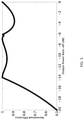
- FIG. 5 illustrates back-off performance of the system of FIG. 4 .
- FIG. 1 illustrates an embodiment of an amplifying device 1 in accordance with the present invention.
- Device 1 comprises four packaged amplifying units 2 A- 2 D, wherein each amplifying unit comprises a respective amplifier 3 A- 3 D.
- Each amplifying unit further comprises a respective matching network 4 A- 4 D.
- amplifying unit 2 A comprises a conductive package substrate 11 A on which a first semiconductor die 14 A and a second semiconductor die 15 A are arranged.
- an RF power transistor is arranged for example a silicon-based laterally diffused metal-oxide-semiconductor (LDMOS) transistor or a Gallium Nitride based field-effect transistor (FET).
- LDMOS laterally diffused metal-oxide-semiconductor
- FET Gallium Nitride based field-effect transistor
- Second semiconductor die 15 A may be a passive die in the sense that it comprises no active elements. More in particular, a capacitor may be arranged on semiconductor die 15 A, such as a metal-oxide-semiconductor (MOS) capacitor or a metal-insulator-metal (MIM) capacitor.
- MOS metal-oxide-semiconductor
- MIM metal-insulator-metal
- Second amplifying unit 2 A comprises a first plurality of bondwires 16 A connecting input lead 13 A to an input terminal of the transistor on first semiconductor die 14 A.
- This connection can be a direct connection, as shown in FIG. 3 , or an indirect connection in which a matching network is arranged in series in between input lead 13 A and the input terminal of the transistor.
- a second plurality of bondwires 17 A is used for connecting the RF power transistor to second semiconductor die 15 A. More in particular, bondwires 17 A connect the output terminal of the RF power transistor to a first terminal of the capacitor arranged on second semiconductor die 15 A. A second terminal of this capacitor may be grounded and may be achieved through the conductive substrate 11 A.
- the first terminal of the capacitor is connected, via a third plurality of bondwires 18 A, to output lead 12 A.
- the amplifier of amplifying unit 2 A is referred to as transistor 3 A.
- the second plurality of bondwires 17 A is represented by inductor L which has an inductance L 1
- the capacitor on second semiconductor die 15 A is represented by capacitor C having a capacitance C 1 .
- bondwires 17 A could extend between the output of the RF power transistor and output lead 12 A
- third bondwires 18 A could extend between output lead 12 A and the first terminal of the capacitor on second semiconductor die 15 A.
- FIG. 3 further shows that fourth packaged amplifying unit 3 D is configured in a similar manner as first packaged amplifying unit.
- fourth amplifying unit 2 D comprises a first plurality of bondwires 16 D connecting input lead 13 D to an input terminal of the transistor on first semiconductor die 14 D.
- This connection can be a direct connection, as shown in FIG. 3 , or an indirect connection in which a matching network is arranged in series in between input lead 13 D and the input terminal of the transistor.
- a second plurality of bondwires 17 D is used for connecting the RF power transistor to second semiconductor die 15 C. More in particular, bondwires 17 D connect the output terminal of the RF power transistor to a first terminal of the capacitor arranged on second semiconductor die 15 C. A second terminal of this capacitor may be grounded and may be achieved through the conductive substrate 11 C.
- the first terminal of the capacitor is connected, via a third plurality of bondwires 18 D, to output lead 12 C.
- the amplifier of amplifying unit 2 D is referred to as transistor 3 D.
- the second plurality of bondwires 17 D is represented by inductor L which has an inductance L 1
- the capacitor on second semiconductor die 15 C is represented by capacitor C having a capacitance C 1 .
- bondwires 17 D could extend between the output of the RF power transistor and output lead 12 C
- third bondwires 18 D could extend between output lead 12 C and the first terminal of the capacitor on second semiconductor die 15 C.
- first amplifier 3 A and fourth amplifier 3 D are substantial identical.
- an identical or substantially identical transistor layout can be used for realizing amplifiers 3 A, 3 D.
- Second and third amplifying units 2 B, 2 C are realized in a single package.
- This package comprises two parallel paths that are arranged similar to amplifying units 3 A, 3 D.
- Each path comprises a separate first semiconductor die, referred to as first semiconductor die 14 B or 14 C, but both paths share the same second semiconductor die 15 B.
- a first plurality of bondwires 16 B connects input lead 13 B to an input terminal of the transistor on second semiconductor die 14 B.
- This connection can be a direct connection, as shown in FIG. 3 , or an indirect connection in which a matching network is arranged in series in between input lead 13 B and the input terminal of the transistor.
- a second plurality of bondwires 17 B is used for connecting the RF power transistor to second semiconductor die 15 B. More in particular, bondwires 17 B connect the output terminal of the RF power transistor to a first terminal of the capacitor arranged on second semiconductor die 15 B. A second terminal of this capacitor may be grounded and may be achieved through the conductive substrate 11 B.
- a first plurality of bondwires 16 C connects input lead 13 C to an input terminal of the transistor on second semiconductor die 14 C.
- This connection can be a direct connection, as shown in FIG. 3 , or an indirect connection in which a matching network is arranged in series in between input lead 13 C and the input terminal of the transistor.
- a second plurality of bondwires 17 C is used for connecting the RF power transistor to second semiconductor die 15 B. More in particular, bondwires 17 C connect the output terminal of the RF power transistor to a first terminal of the capacitor arranged on second semiconductor die 15 B. A second terminal of this capacitor may be grounded and may be achieved through the conductive substrate 11 B.
- the first terminal of the capacitor is connected, via a third plurality of bondwires 18 B, 18 C to output lead 12 B.
- the amplifiers of amplifying units 2 B, 2 C are referred to as transistor 3 B, 3 C, respectively.
- the second plurality of bondwires 17 B is represented by inductor L+ which has an inductance equaling L 1 +dL
- the third plurality of bondwires 17 C is represented by inductor L ⁇ dL which has an inductance equaling L 1 ⁇ dL
- the capacitor on second semiconductor die 15 B is represented by capacitor 2 C having a capacitance that equals 2C1.
- bondwires 17 B, 17 C could extend between the output of the RF power transistor on first semiconductor die 14 B, 14 C, respectively, and output lead 12 B, and third bondwires 18 B, 18 C could extend between output lead 12 B and the first terminal of the capacitor on second semiconductor die 15 B.
- second amplifier 3 B and third amplifier 3 C are substantial identical.
- an identical or substantially identical transistor layout can be used for realizing amplifiers 3 B, 3 C.
- second amplifiers 3 A- 3 D could all be substantial identical.
- device 1 comprises an input splitter 10 A arranged between the first input (“input 1 ”) and the input terminals of amplifiers 3 A, 3 B, and an input splitter 10 B arranged between the second input (“input 2 ”) and the input terminals of amplifiers 3 C, 3 D.
- Input splitter 10 A introduces a phase delay of 90 degrees in the signal fed to amplifier 3 B relative to the signal fed to amplifier 3 A.
- input splitter 10 B introduces a phase delay of 90 degrees in the signal fed to amplifier 3 C relative to the signal fed to amplifier 3 D.
- input splitters 10 A, 10 B shown in FIGS. 2 and 3 are represented by an ideal splitter for which one output branch comprises a 90 degrees phase shifter 7 A, 7 B.
- amplifying units 3 A and 3 D are connected via respective impedance inverters 5 A, 5 B to combining node C. This latter node is also connected to the outputs of amplifying units 3 B, 3 C and to load 8 via an optional impedance inverter 6 .
- Impedance inverters 6 , 5 A, 5 B can be realized using quarter-wave length transmission lines, for example realized on printed circuit board.
- phase delay introduced by the matching networks 4 A- 4 D substantially equals 90 degrees. It can then be verified that the phase delay between the first input and combining node C is identical irrespective of the path followed. The same holds for the phase delay between the second input and combining node C.
- a value for C 1 is chosen such that the fundamental and harmonic admittances seen by amplifiers 3 A- 3 D correspond to the so-called quasi-load insensitive class E configuration.
- Device 1 is operable in two modes.
- first amplifier 3 A and fourth amplifier 3 D are off and second amplifier 3 B and third amplifier 3 C cooperate to form an outphasing amplifier.
- the signals fed at the two inputs have substantially the same amplitude but differ in phase.
- These signals can for instance be generated using a dedicated signal unit on the basis of a signal to be amplified.
- the signals to be fed to the first input and second input are constant envelope signals different in phase by an amount equal to 2 ⁇ , wherein ⁇ is referred to as the outphasing angle.
- ⁇ is referred to as the outphasing angle.
- Chireix compensating elements are used. More in particular, the Chireix compensating elements are configured compensate for reactive impedances seen by the second amplifier 3 B and third amplifier 3 C. It should be noted that the reactive impedances generally vary with the outphasing angle.
- the compensating elements are therefore usually designed by optimizing performance, e.g. efficiency, over a certain back off power range.
- the actual design of Chireix compensating elements is well known in the art, see for example the PhD thesis “High Efficiency RF Power Amplifier Architectures” by Qureshi et al, TU Delft, 2012, ISBN 978-94-6203-071-8.
- an outphasing amplifier is formed using amplifiers 3 B, 3 C and matching networks 4 B, 4 C.
- matching networks 4 B, 4 C each preferably correspond to a QLI class E matching network comprising a series inductor and a shunt capacitor in which, for each matching network, a respective Chireix compensating elements is integrated by varying the inductance of the series inductor. More in particular, the inductance value is changed by varying at least one of a shape, height, and length of the bondwire. In this manner, a low-complexity matching network can be obtained by which a high bandwidth can be obtained when compared to other topologies in which more bandwidth sensitive components are used.
- the capacitance of the shunt capacitor can be represented by C 1 .
- second and third amplifiers 3 B, 3 C are within the same package. This allows the shunt capacitors to be combined on a single semiconductor die 15 B, resulting in a capacitor having a capacitance equal to 2C1. It should be noted that the present invention does not exclude embodiments wherein amplifiers 3 B, 3 C are integrated on the same semiconductor die.
- amplifiers 3 A- 3 D are substantially identical, the same inductance and capacitance values, i.e. L 1 and C 1 , can be used for matching network 4 A and matching network 4 D.
- the present invention does however not exclude embodiments wherein amplifiers 3 A, 3 D are different from 3 B, 3 C.
- amplifiers 3 A, 3 D can be configured to output higher powers than amplifiers 3 B, 3 C.
- Impedance inverters 5 A, 5 B introduce the impedance modulation that is required in DPAs.
- Inverters 5 A. 5 B are arranged in between amplifiers 3 A, 3 D, which act as peak amplifiers of the DPAs in the Doherty mode, and combining node C.
- the configuration can be referred to as an inverted DPA.
- the phase delay elements in the input part of device 1 it is ensured that the signals amplified by amplifiers 3 A- 3 D all add up in phase at combining node C.
- amplifiers 3 A, 3 D are preferably biased in class C. This would ensure that amplifiers 3 A, 3 D only become operational at relatively high input powers.
- Amplifiers 3 B, 3 C are preferable biased in class AB or class B.
- FIG. 4 illustrates an amplifying system 100 in accordance with the present invention.
- System 100 comprises an amplifying device 1 as illustrated in FIGS. 1-4 , and a signal unit 40 for generating the signals to be fed to the first and second inputs.
- Signal unit 40 is controlled by a controller 41 , which is connected to a memory 42 .
- a first signal to be fed to the first input of amplifying device 1 and a second signal to be fed to the second input of amplifying device 1 generally have a time-varying amplitude and phase offset.
- Amax the maximum amplitude
- ⁇ (t) cos ⁇ 1 (A(t)/Amax) the outphasing angle.
- ⁇ (t) can be set to a constant value, e.g. 0.
- output power refers to the momentary output power associated with the modulated carrier.
- different operational modes may be selected depending on the desired momentary value of the amplitude of the modulated signal.
- signal unit 40 can be implemented digitally. In other implementations, signal unit 40 receives a non-modulated carrier signal from which it derives the signals for the first and second inputs of the amplifying device 1 .
- FIG. 5 illustrates an overview of the efficiency of amplifying system 100 as a function of output power.
- output powers below ⁇ 14 dB back off the linear mode is used, for output powers between ⁇ 14 dB and ⁇ 6 dB back off the outphasing mode, and for output powers larger than ⁇ 6 dB back off the Doherty mode.
- the amplifying device and system of the present invention allow high efficiencies to be reached under large power back-off. This has been realized using an efficient integration of Chireix compensating elements and QLI class E matching networks and implementing these techniques in an amplifier line-up that allows multiple modes of operation.
Landscapes
- Engineering & Computer Science (AREA)
- Power Engineering (AREA)
- Computer Networks & Wireless Communication (AREA)
- Signal Processing (AREA)
- Microelectronics & Electronic Packaging (AREA)
- Amplifiers (AREA)
Abstract
Description
Claims (19)
Applications Claiming Priority (2)
| Application Number | Priority Date | Filing Date | Title |
|---|---|---|---|
| NL2022750 | 2019-03-15 | ||
| NL2022750A NL2022750B1 (en) | 2019-03-15 | 2019-03-15 | Amplifying device and amplifying system comprising the same |
Publications (2)
| Publication Number | Publication Date |
|---|---|
| US20200295714A1 US20200295714A1 (en) | 2020-09-17 |
| US11245364B2 true US11245364B2 (en) | 2022-02-08 |
Family
ID=66476787
Family Applications (1)
| Application Number | Title | Priority Date | Filing Date |
|---|---|---|---|
| US16/817,811 Active 2040-06-05 US11245364B2 (en) | 2019-03-15 | 2020-03-13 | Amplifying device and amplifying system comprising the same |
Country Status (4)
| Country | Link |
|---|---|
| US (1) | US11245364B2 (en) |
| EP (1) | EP3709353B1 (en) |
| CN (1) | CN111697981B (en) |
| NL (1) | NL2022750B1 (en) |
Families Citing this family (2)
| Publication number | Priority date | Publication date | Assignee | Title |
|---|---|---|---|---|
| US11936342B2 (en) | 2021-05-06 | 2024-03-19 | Macom Technology Solutions Holdings, Inc. | Output-integrated transistor amplifier device packages incorporating internal connections |
| NL2031173B1 (en) * | 2022-03-07 | 2023-09-11 | Ampleon Netherlands Bv | Rf amplifier and electronic device comprising the same |
Family Cites Families (3)
| Publication number | Priority date | Publication date | Assignee | Title |
|---|---|---|---|---|
| CN104993796B (en) * | 2015-06-25 | 2018-03-27 | 江苏大学 | A kind of Doherty power amplifier |
| US9882535B2 (en) * | 2016-06-28 | 2018-01-30 | Infineon Technologies Ag | Doherty-Chireix combined amplifier |
| CN109450383A (en) * | 2018-11-27 | 2019-03-08 | 江苏大学 | A kind of broadband dual-frequency section Doherty power amplifier based on phase delay double frequency output matching network |
-
2019
- 2019-03-15 NL NL2022750A patent/NL2022750B1/en not_active IP Right Cessation
-
2020
- 2020-03-10 EP EP20162100.0A patent/EP3709353B1/en active Active
- 2020-03-13 US US16/817,811 patent/US11245364B2/en active Active
- 2020-03-16 CN CN202010181500.5A patent/CN111697981B/en active Active
Non-Patent Citations (6)
| Title |
|---|
| Grebennikov, A.,"Broadband PA Techniques for Efficiency Enhancement" IEEE MTT-S 2014 Power Amplifier Symposium. (Year: 2014). * |
| Hakala et al., "A 2.14-GHz Chireix Outphasing Transmitter," IEEE Transactions on Microwave Theory and Techniques, vol. 53, No. 6, pp. 2129-2138 (2005). |
| NL Search Report and Written Opinion, NL Application No. 2022750, dated Dec. 13, 2019, 27 pages. |
| Qureshi et al., "A 112W GaN Dual Input Doherty-Outphasing Power amplifier," IEEE MTT-S International Microwave Symposium (2016). |
| Qureshi et al., "High Efficiency and Wide Bandwidth Quasi-Load Insensitive Class-E Operation Utilizing Package Integration," IEEE Transactions on Microwave Theory and Techniques (2018). |
| Qureshi, "High Efficiency RF Power Amplifier Architectures," TU Delft, ISBN 978-94-6203-071-8 (2012). |
Also Published As
| Publication number | Publication date |
|---|---|
| CN111697981A (en) | 2020-09-22 |
| CN111697981B (en) | 2023-01-20 |
| US20200295714A1 (en) | 2020-09-17 |
| NL2022750B1 (en) | 2020-09-22 |
| EP3709353A1 (en) | 2020-09-16 |
| EP3709353B1 (en) | 2022-01-05 |
Similar Documents
| Publication | Publication Date | Title |
|---|---|---|
| US7064606B2 (en) | High efficiency amplifier and method of designing same | |
| CN108259008B (en) | Doherty Amplifier with Passive Phase Compensation Circuit | |
| CN113949347B (en) | Load Modulation Amplifier | |
| Kang et al. | Design of bandwidth-enhanced Doherty power amplifiers for handset applications | |
| US8228123B2 (en) | Integrated Doherty amplifier | |
| CN107528554B (en) | Compact Hirak combiner and impedance matching circuit | |
| CN109327191B (en) | Four-way doherty amplifier and mobile communication base station | |
| KR101123505B1 (en) | High efficiency amplifier and method of designing same | |
| US7884668B2 (en) | Integrated doherty type amplifier arrangement with high power efficiency | |
| US20100001802A1 (en) | Integrated doherty type amplifier arrangement with high power efficiency | |
| US8963644B2 (en) | Reconfigurable output matching network for multiple power mode power amplifiers | |
| WO2017028563A1 (en) | Symmetry doherty power amplification circuit apparatus and power amplifier | |
| CN106664062B (en) | Integrated 3-way Doherty amplifier | |
| Kang et al. | Design of Doherty power amplifiers for handset applications | |
| US12537484B2 (en) | RF amplifier and electronic device comprising the same | |
| US10630242B2 (en) | Doherty amplifiers with passive phase compensation circuits | |
| US20240291437A1 (en) | Doherty power amplifier | |
| US11245364B2 (en) | Amplifying device and amplifying system comprising the same | |
| US12199571B2 (en) | Hybrid Doherty power amplifier module | |
| JP2006515723A (en) | Multiband signal processing apparatus, processing method and product | |
| JP5800360B2 (en) | Doherty amplifier | |
| WO2022172868A1 (en) | Power amplification circuit | |
| US20250105799A1 (en) | Compact Doherty Amplifier Having Improved Video Bandwidth | |
| US11967936B2 (en) | Output-integrated transistor device packages | |
| CN119154809A (en) | Radio frequency power amplifying circuit based on doherty amplifier |
Legal Events
| Date | Code | Title | Description |
|---|---|---|---|
| FEPP | Fee payment procedure |
Free format text: ENTITY STATUS SET TO UNDISCOUNTED (ORIGINAL EVENT CODE: BIG.); ENTITY STATUS OF PATENT OWNER: LARGE ENTITY |
|
| STPP | Information on status: patent application and granting procedure in general |
Free format text: APPLICATION DISPATCHED FROM PREEXAM, NOT YET DOCKETED |
|
| AS | Assignment |
Owner name: AMPLEON NETHERLANDS B.V., NETHERLANDS Free format text: ASSIGNMENT OF ASSIGNORS INTEREST;ASSIGNORS:QURESHI, ABDUL RAHEEM;PIRES, SERGIO CARLOS DA CONCEICAO;SIGNING DATES FROM 20200326 TO 20200502;REEL/FRAME:053314/0976 |
|
| STPP | Information on status: patent application and granting procedure in general |
Free format text: DOCKETED NEW CASE - READY FOR EXAMINATION |
|
| STPP | Information on status: patent application and granting procedure in general |
Free format text: NON FINAL ACTION MAILED |
|
| STPP | Information on status: patent application and granting procedure in general |
Free format text: RESPONSE TO NON-FINAL OFFICE ACTION ENTERED AND FORWARDED TO EXAMINER |
|
| STPP | Information on status: patent application and granting procedure in general |
Free format text: NOTICE OF ALLOWANCE MAILED -- APPLICATION RECEIVED IN OFFICE OF PUBLICATIONS |
|
| STPP | Information on status: patent application and granting procedure in general |
Free format text: PUBLICATIONS -- ISSUE FEE PAYMENT VERIFIED |
|
| STCF | Information on status: patent grant |
Free format text: PATENTED CASE |
|
| MAFP | Maintenance fee payment |
Free format text: PAYMENT OF MAINTENANCE FEE, 4TH YEAR, LARGE ENTITY (ORIGINAL EVENT CODE: M1551); ENTITY STATUS OF PATENT OWNER: LARGE ENTITY Year of fee payment: 4 |