US11245335B2 - DC/DC converter - Google Patents
DC/DC converter Download PDFInfo
- Publication number
- US11245335B2 US11245335B2 US16/662,629 US201916662629A US11245335B2 US 11245335 B2 US11245335 B2 US 11245335B2 US 201916662629 A US201916662629 A US 201916662629A US 11245335 B2 US11245335 B2 US 11245335B2
- Authority
- US
- United States
- Prior art keywords
- voltage
- region
- low
- pair
- side switching
- Prior art date
- Legal status (The legal status is an assumption and is not a legal conclusion. Google has not performed a legal analysis and makes no representation as to the accuracy of the status listed.)
- Active, expires
Links
Images


Classifications
-
- H—ELECTRICITY
- H02—GENERATION; CONVERSION OR DISTRIBUTION OF ELECTRIC POWER
- H02M—APPARATUS FOR CONVERSION BETWEEN AC AND AC, BETWEEN AC AND DC, OR BETWEEN DC AND DC, AND FOR USE WITH MAINS OR SIMILAR POWER SUPPLY SYSTEMS; CONVERSION OF DC OR AC INPUT POWER INTO SURGE OUTPUT POWER; CONTROL OR REGULATION THEREOF
- H02M1/00—Details of apparatus for conversion
-
- H—ELECTRICITY
- H02—GENERATION; CONVERSION OR DISTRIBUTION OF ELECTRIC POWER
- H02M—APPARATUS FOR CONVERSION BETWEEN AC AND AC, BETWEEN AC AND DC, OR BETWEEN DC AND DC, AND FOR USE WITH MAINS OR SIMILAR POWER SUPPLY SYSTEMS; CONVERSION OF DC OR AC INPUT POWER INTO SURGE OUTPUT POWER; CONTROL OR REGULATION THEREOF
- H02M3/00—Conversion of DC power input into DC power output
- H02M3/02—Conversion of DC power input into DC power output without intermediate conversion into AC
- H02M3/04—Conversion of DC power input into DC power output without intermediate conversion into AC by static converters
- H02M3/10—Conversion of DC power input into DC power output without intermediate conversion into AC by static converters using discharge tubes with control electrode or semiconductor devices with control electrode
- H02M3/145—Conversion of DC power input into DC power output without intermediate conversion into AC by static converters using discharge tubes with control electrode or semiconductor devices with control electrode using devices of a triode or transistor type requiring continuous application of a control signal
- H02M3/155—Conversion of DC power input into DC power output without intermediate conversion into AC by static converters using discharge tubes with control electrode or semiconductor devices with control electrode using devices of a triode or transistor type requiring continuous application of a control signal using semiconductor devices only
- H02M3/156—Conversion of DC power input into DC power output without intermediate conversion into AC by static converters using discharge tubes with control electrode or semiconductor devices with control electrode using devices of a triode or transistor type requiring continuous application of a control signal using semiconductor devices only with automatic control of output voltage or current, e.g. switching regulators
- H02M3/158—Conversion of DC power input into DC power output without intermediate conversion into AC by static converters using discharge tubes with control electrode or semiconductor devices with control electrode using devices of a triode or transistor type requiring continuous application of a control signal using semiconductor devices only with automatic control of output voltage or current, e.g. switching regulators including plural semiconductor devices as final control devices for a single load
- H02M3/1588—Conversion of DC power input into DC power output without intermediate conversion into AC by static converters using discharge tubes with control electrode or semiconductor devices with control electrode using devices of a triode or transistor type requiring continuous application of a control signal using semiconductor devices only with automatic control of output voltage or current, e.g. switching regulators including plural semiconductor devices as final control devices for a single load comprising at least one synchronous rectifier element
-
- H01L23/645—
-
- H01L25/18—
-
- H—ELECTRICITY
- H05—ELECTRIC TECHNIQUES NOT OTHERWISE PROVIDED FOR
- H05K—PRINTED CIRCUITS; CASINGS OR CONSTRUCTIONAL DETAILS OF ELECTRIC APPARATUS; MANUFACTURE OF ASSEMBLAGES OF ELECTRICAL COMPONENTS
- H05K7/00—Constructional details common to different types of electric apparatus
- H05K7/14—Mounting supporting structure in casing or on frame or rack
- H05K7/1438—Back panels or connecting means therefor; Terminals; Coding means to avoid wrong insertion
- H05K7/1447—External wirings; Wiring ducts; Laying cables
- H05K7/1451—External wirings; Wiring ducts; Laying cables with connections between circuit boards or units
-
- H—ELECTRICITY
- H10—SEMICONDUCTOR DEVICES; ELECTRIC SOLID-STATE DEVICES NOT OTHERWISE PROVIDED FOR
- H10W—GENERIC PACKAGES, INTERCONNECTIONS, CONNECTORS OR OTHER CONSTRUCTIONAL DETAILS OF DEVICES COVERED BY CLASS H10
- H10W44/00—Electrical arrangements for controlling or matching impedance
- H10W44/501—Inductive arrangements
-
- H—ELECTRICITY
- H10—SEMICONDUCTOR DEVICES; ELECTRIC SOLID-STATE DEVICES NOT OTHERWISE PROVIDED FOR
- H10W—GENERIC PACKAGES, INTERCONNECTIONS, CONNECTORS OR OTHER CONSTRUCTIONAL DETAILS OF DEVICES COVERED BY CLASS H10
- H10W90/00—Package configurations
-
- H—ELECTRICITY
- H01—ELECTRIC ELEMENTS
- H01F—MAGNETS; INDUCTANCES; TRANSFORMERS; SELECTION OF MATERIALS FOR THEIR MAGNETIC PROPERTIES
- H01F27/00—Details of transformers or inductances, in general
- H01F27/24—Magnetic cores
-
- H—ELECTRICITY
- H01—ELECTRIC ELEMENTS
- H01F—MAGNETS; INDUCTANCES; TRANSFORMERS; SELECTION OF MATERIALS FOR THEIR MAGNETIC PROPERTIES
- H01F41/00—Apparatus or processes specially adapted for manufacturing or assembling magnets, inductances or transformers; Apparatus or processes specially adapted for manufacturing materials characterised by their magnetic properties
- H01F41/02—Apparatus or processes specially adapted for manufacturing or assembling magnets, inductances or transformers; Apparatus or processes specially adapted for manufacturing materials characterised by their magnetic properties for manufacturing cores, coils, or magnets
- H01F41/04—Apparatus or processes specially adapted for manufacturing or assembling magnets, inductances or transformers; Apparatus or processes specially adapted for manufacturing materials characterised by their magnetic properties for manufacturing cores, coils, or magnets for manufacturing coils
- H01F41/041—Printed circuit coils
-
- H01L21/30—
-
- H01L27/06—
-
- H—ELECTRICITY
- H02—GENERATION; CONVERSION OR DISTRIBUTION OF ELECTRIC POWER
- H02M—APPARATUS FOR CONVERSION BETWEEN AC AND AC, BETWEEN AC AND DC, OR BETWEEN DC AND DC, AND FOR USE WITH MAINS OR SIMILAR POWER SUPPLY SYSTEMS; CONVERSION OF DC OR AC INPUT POWER INTO SURGE OUTPUT POWER; CONTROL OR REGULATION THEREOF
- H02M3/00—Conversion of DC power input into DC power output
- H02M3/003—Constructional details, e.g. physical layout, assembly, wiring or busbar connections
Definitions
- the present invention relates to a DC/DC converter.
- a switching converter control circuit configured to perform rectification by alternately turning on a first switch and a second switch is disclosed as a conventional DC/DC converter used in various kinds of usage.
- the switching converter control circuit includes a plurality of first drive units, a second drive unit, and a selection unit.
- the first drive units drive a plurality of first switches, respectively.
- the second drive unit drives a second switch.
- the selection unit stops some of the first drive units in accordance with load current, input voltage, output voltage, or the difference between the input and output voltages.
- a switching converter control circuit disclosed in Japanese Patent Application Laid-open No. 2006-296186 has room for further improvement in versatility.
- the present invention is intended to solve the above-described problem and provide a DC/DC converter having improved versatility.
- a DC/DC converter includes electronic components group including a first capacitor, a high-voltage-side switching element, a low-voltage-side switching element, an inductor, and a second capacitor and forming a half-bridge circuit; and a substrate including a high-voltage region in which a high-voltage wiring pattern having a relatively high voltage is formed, a low-voltage region in which a low-voltage wiring pattern having a relatively low voltage is formed, a connection region in which a connection wiring pattern is formed, and a pair of ground regions in each of which a ground pattern is formed, wherein the connection region is positioned between the high-voltage region and the low-voltage region in a first direction and adjacent to the high-voltage region and the low-voltage region, the pair of ground regions are positioned adjacent to the high-voltage region, the connection region, and the low-voltage region with the high-voltage region, the connection region, and the low-voltage region
- the substrate includes a first mounting surface and a second mounting surface different from the first mounting surface, the high-voltage region, the low-voltage region, the connection region, and the pair of ground regions being formed on the first mounting surface, signal transmission patterns configured to transmit drive signals for driving the high-voltage-side switching element and the low-voltage-side switching element being formed on the second mounting surface, and the high-voltage-side switching element and the low-voltage-side switching element have gate terminals connected with the signal transmission patterns.
- a plurality of the first capacitors are provided, one of the first capacitors is mounted across one of the pair of ground regions and the high-voltage region, and another one of the first capacitors is mounted across the other of the pair of ground regions and the high-voltage region, a plurality of the high-voltage-side switching elements are provided and all of the high-voltage-side switching elements mounted across the high-voltage region and the connection region, a plurality of the low-voltage-side switching elements are provided, one of the low-voltage-side switching elements is mounted across the connection region and the one of the pair of ground regions, and another one of the low-voltage-side switching elements is mounted across the connection region and the other of the pair of ground regions, and a plurality of the second capacitors are provided, one of the second capacitors is mounted across the low-voltage region and the one of the pair of ground regions, and another one of the second capacitors is mounted across the low-voltage region
- the substrate is provided with a plurality of unit pattern region groups each including the single high-voltage region, the single low-voltage region, the single connection region, and the pair of ground regions.
- the DC/DC converter it is possible to configure that the low-voltage regions of the plurality of unit pattern region groups adjacent to each other in the first direction are positioned adjacent to each other in the first direction.
- FIG. 1 is an outline configuration diagram illustrating a schematic configuration of a DC/DC converter according to an embodiment
- FIG. 2 is a schematic block diagram illustrating an artwork of a substrate included in the DC/DC converter according to the embodiment
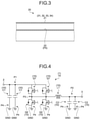
- FIG. 3 is a schematic cross-sectional view for description of mounting surfaces of the substrate included in the DC/DC converter according to the embodiment
- FIG. 4 is a schematic configuration diagram illustrating another configuration of the DC/DC converter according to the embodiment.
- FIG. 5 is a schematic block diagram illustrating another artwork of the substrate included in the DC/DC converter according to the embodiment.
- FIG. 6 is a schematic block diagram illustrating another artwork of the substrate included in the DC/DC converter according to the embodiment.
- a DC/DC converter 1 illustrated in FIG. 1 transforms the voltage of direct-current power input through an input terminal 2 , and outputs the direct-current power toward an output terminal 3 .
- the input terminal 2 and the output terminal 3 are each connected with a power source instrument such as an electrical generator or an electrical storage device, or with an electrical instrument driven by electrical power.
- a step-down DC/DC converter circuit of a synchronous rectification scheme is formed by electronic components group 10 connecting the input terminal 2 and the output terminal 3 .
- the DC/DC converter 1 includes the electronic components group 10 including a first capacitor C 1 , a high-voltage-side switching element Q 1 , a low-voltage-side switching element Q 2 , an inductor L 1 , and a second capacitor C 2 .
- the electronic components group 10 form a half-bridge circuit.
- the first capacitor C 1 is a passive element capable of accumulating and discharging electric charge, and is a smoothing capacitor.
- the first capacitor C 1 has one terminal connected with a ground GND and the other terminal connected with the input terminal 2 and the drain terminal of the high-voltage-side switching element Q 1 .
- the high-voltage-side switching element Q 1 and the low-voltage-side switching element Q 2 may be each a field effect transistor (FET).
- FET field effect transistor
- the high-voltage-side switching element Q 1 has the drain terminal connected with the input terminal 2 and the other terminal of the first capacitor C 1 , the source terminal connected with one terminal of the inductor L 1 and the drain terminal of the low-voltage-side switching element Q 2 , and the gate terminal connected with a controller 4 .
- the low-voltage-side switching element Q 2 has the drain terminal connected with the source terminal of the high-voltage-side switching element Q 1 and the one terminal of the inductor L 1 , the source terminal connected with the ground GND, and the gate terminal connected with the controller 4 .
- the inductor L 1 is a passive element capable of accumulating energy in a magnetic field formed by flowing current.
- the second capacitor C 2 is a passive element capable of accumulating and discharging electric charge.
- the inductor L 1 and the second capacitor C 2 form a LC smoothing circuit.
- the one terminal of the inductor L 1 is connected with the source terminal of the high-voltage-side switching element Q 1 and the drain terminal of the low-voltage-side switching element Q 2 , and the other terminal of the inductor L 1 is connected with one terminal of the second capacitor C 2 and the output terminal 3 .
- the second capacitor C 2 has the one terminal connected with the other terminal of the inductor L 1 and the output terminal 3 and the other terminal connected with the ground GND.
- the controller 4 controls switching operation by transmitting, to the high-voltage-side switching element Q 1 and the low-voltage-side switching element Q 2 , drive signals for driving these elements.
- the DC/DC converter 1 converts an input voltage of direct-current power from the input terminal 2 into a predetermined output voltage through control of the duty duration (ON duration) of the high-voltage-side switching element Q 1 and the low-voltage-side switching element Q 2 by the controller 4 , and then outputs the direct-current power through the output terminal 3 .
- the DC/DC converter 1 includes a substrate 20 on which the above-described electronic components group 10 are mounted and form a half-bridge circuit.
- the DC/DC converter 1 according to the present embodiment achieves improved versatility by contriving artwork (substrate pattern designing) of the substrate 20 as illustrated in FIG. 2 .
- the substrate 20 provides an electronic circuit on which the electronic components group 10 are mounted and electrically connected with each other.
- the substrate 20 is what is called a printed circuit board (PCB).
- the substrate 20 has a circuit body formed by a wiring pattern (print pattern) made of conductive material such as copper and printed on an insulating layer made of insulating material such as epoxy resin, glass epoxy resin, paper epoxy resin, or ceramic.
- the electronic components group 10 are mounted on the substrate 20 by electrically connecting the terminals of the electronic components group 10 with the circuit body by soldering or the like.
- the circuit body of the substrate 20 electrically connects the electronic components group 10 to form a circuit system in accordance with a function requested as the DC/DC converter 1 .
- the substrate 20 may be a multi-layer object (in other words, a multi-layer substrate) formed by stacking a plurality of insulating layers on each of which a wiring pattern is printed.
- the substrate 20 is formed substantially in a rectangular plate shape.
- the substrate 20 includes a high-voltage region 31 , a low-voltage region 32 , a connection region 33 , and a pair of ground regions 34 .
- the high-voltage region 31 is a region in which a high-voltage wiring pattern P 1 (refer to FIG. 1 ) having a relatively high voltage is formed.
- the input terminal 2 is connected with the high-voltage wiring pattern P 1 .
- the low-voltage region 32 is a region in which a low-voltage wiring pattern P 2 (refer to FIG. 1 ) having a relatively low voltage is formed.
- the output terminal 3 is connected with the low-voltage wiring pattern P 2 .
- the connection region 33 is a region in which a connection wiring pattern P 3 (refer to FIG. 1 ) is formed as a wiring pattern interposed between the high-voltage wiring pattern P 1 and the low-voltage wiring pattern P 2 .
- the ground regions 34 is a region in which a ground pattern P 4 connected with the ground GND is formed.
- connection region 33 is positioned between the high-voltage region 31 and the low-voltage region 32 in a first direction X.
- the connection region 33 is positioned adjacent to the high-voltage region 31 and the low-voltage region 32 in the first direction X.
- the high-voltage region 31 and the low-voltage region 32 are positioned on the respective sides of the connection region 33 to sandwich them in the first direction X.
- the high-voltage region 31 and the low-voltage region 32 are each positioned adjacent to the connection region 33 .
- the high-voltage region 31 , the connection region 33 , and the low-voltage region 32 are positioned side by side adjacent to each other in the stated order from one side to the other side in the first direction X.
- the pair of ground regions 34 are positioned with the high-voltage region 31 , the connection region 33 , and the low-voltage region 32 interposed therebetween in a second direction Y orthogonal (intersecting) to the first direction X.
- the pair of ground regions 34 are positioned adjacent to the high-voltage region 31 , the connection region 33 , and the low-voltage region 32 in the second direction Y.
- the pair of ground regions 34 are positioned on the respective sides of the high-voltage region 31 , the connection region 33 , and the low-voltage region 32 to sandwich them in the second direction Y.
- connection region 33 is formed as a substantially rectangular region sandwiched between the high-voltage region 31 and the low-voltage region 32 .
- Each ground region 34 is formed as a substantially rectangular band region along the first direction X.
- the high-voltage region 31 and the low-voltage region 32 are formed as substantially T-shaped regions.
- Each ground region 34 is sandwiched between parts of the high-voltage region 31 and the low-voltage region 32 in the first direction X.
- an end part of each of the high-voltage region 31 and the low-voltage region 32 which is opposite to the connection region 33 side in the first direction X extends to outside edges (opposite to the connection region 33 side) of the ground regions 34 in the second direction Y.
- the pair of ground regions 34 sandwich parts of the high-voltage region 31 and the low-voltage region 32 in the second direction Y, and are sandwiched between other parts of the high-voltage region 31 and the low-voltage region 32 in the first direction X.
- the first capacitor C 1 is mounted across any one of the pair of ground regions 34 and the high-voltage region 31 .
- the first capacitor C 1 has the one terminal connected with the ground pattern P 4 and the other terminal connected with the high-voltage wiring pattern P 1 .
- the high-voltage-side switching element Q 1 is mounted across the high-voltage region 31 and the connection region 33 .
- the high-voltage-side switching element Q 1 has the drain terminal connected with the high-voltage wiring pattern P 1 and the source terminal connected with the connection wiring pattern P 3 .
- the low-voltage-side switching element Q 2 is mounted across the connection region 33 and one of the pair of ground regions 34 .
- the low-voltage-side switching element Q 2 has the drain terminal connected with the connection wiring pattern P 3 and the source terminal connected with the ground pattern P 4 .
- the inductor L 1 is mounted across the connection region 33 and the low-voltage region 32 .
- the inductor L 1 has the one terminal connected with the connection wiring pattern P 3 and the other terminal connected with the low-voltage wiring pattern P 2 .
- the second capacitor C 2 is mounted across the low-voltage region 32 and one of the pair of ground regions 34 .
- the second capacitor C 2 has the one terminal connected with the low-voltage wiring pattern P 2 and the other terminal connected with the ground pattern P 4 .
- the substrate 20 includes a first mounting surface 21 on which the high-voltage region 31 , the low-voltage region 32 , the connection region 33 , and the pair of ground regions 34 are formed, and a second mounting surface 22 different from the first mounting surface 21 .
- the above-described electronic components group 10 are mounted on the first mounting surface 21 .
- Signal transmission patterns P 5 (refer to FIG. 1 ) configured to transmit drive signals for driving the high-voltage-side switching element Q 1 and the low-voltage-side switching element Q 2 is formed on the second mounting surface 22 .
- the high-voltage-side switching element Q 1 and the low-voltage-side switching element Q 2 are connected with the signal transmission patterns P 5 to be capable of receiving the drive signals from the controller 4 through the signal transmission patterns P 5 .
- the first mounting surface 21 according to the present embodiment is a mounting surface positioned at the outermost surface of the substrate 20 .
- the second mounting surface 22 according to the present embodiment is a mounting surface positioned at an inner layer of the substrate 20 .
- the gate terminals of the high-voltage-side switching element Q 1 and the low-voltage-side switching element Q 2 according to the present embodiment are each connected with the signal transmission patterns P 5 on the second mounting surface 22 as the inner layer of the substrate 20 through a through-hole, a via, or the like.
- the DC/DC converter 1 can have a wiring pattern disposition having high versatility in designing, and thus have improved versatility.
- a DC/DC converter 1 A illustrated in FIGS. 4 and 5 is provided with a plurality of the first capacitors C 1 , a plurality of the high-voltage-side switching elements Q 1 , a plurality of the low-voltage-side switching elements Q 2 , and a plurality of the second capacitors C 2 .
- the DC/DC converter 1 A is provided with the two first capacitors C 1 in parallel, the two high-voltage-side switching elements Q 1 in parallel, the two low-voltage-side switching elements Q 2 in parallel, and the two second capacitors C 2 in parallel.
- one of the first capacitors C 1 is mounted across one of the pair of ground regions 34 and the high-voltage region 31
- the other first capacitor C 1 is mounted across the other of the pair of ground regions 34 and the high-voltage region 31
- the high-voltage-side switching elements Q 1 are both mounted across the high-voltage region 31 and the connection region 33
- One of the low-voltage-side switching elements Q 2 is mounted across the connection region 33 and one of the pair of ground regions 34
- the other low-voltage-side switching element Q 2 is mounted across the connection region 33 and the other of the pair of ground regions 34
- One of the second capacitors C 2 is mounted across the low-voltage region 32 and one of the pair of ground regions 34
- the other second capacitor C 2 is mounted across the low-voltage region 32 and the other of the pair of ground regions 34 .
- the DC/DC converter 1 A configured as described above can have an artwork similar to that of the above-described DC/DC converter 1 in designing (refer to FIGS. 2 and 5 ).
- a DC/DC converter 1 B illustrated in FIG. 6 is a multi-phase converter in which a plurality of half-bridge circuits each forming a step-down DC/DC converter circuit are connected in parallel to achieve high power outputting.
- the substrate 20 included in the DC/DC converter 1 B illustrated in FIG. 6 is provided with a plurality of unit pattern region groups 40 each including the single high-voltage region 31 , the single low-voltage region 32 , the single connection region 33 , and the pair of ground regions 34 .
- each unit pattern region group 40 is provided with the single inductor L 1 , the two first capacitors C 1 in parallel, the two high-voltage-side switching elements Q 1 in parallel, the two low-voltage-side switching elements Q 2 in parallel, and the two second capacitors C 2 in parallel.
- the DC/DC converter 1 B is a converter including a total of six unit pattern region groups 40 , two arranged in the first direction X and three arranged in the second direction Y, and capable of performing six-phase operation.
- the low-voltage regions 32 of the unit pattern region groups 40 adjacent to each other in the first direction X are adjacent to and continuous with each other in the first direction X. Accordingly, in this case, in the substrate 20 , the high-voltage region 31 , the connection region 33 , the low-voltage region 32 , the connection region 33 , and the high-voltage region 31 are positioned side by side adjacent to each other in the stated order from one side to the other side in the first direction X. In the DC/DC converter 1 B, parts of the high-voltage and low-voltage regions 31 and 32 of the unit pattern region groups 40 adjacent to each other in the second direction Y are adjacent to and continuous with each other in the second direction Y. In the DC/DC converter 1 B, one of the pair of ground regions 34 of each of the unit pattern region groups 40 adjacent to each other in the second direction Y is shared.
- the DC/DC converter 1 B configured as described above can have an artwork similar to that of the above-described DC/DC converter 1 in designing (refer to FIGS. 2 and 6 ).
- the electronic components group 10 including the first capacitor C 1 , the high-voltage-side switching element Q 1 , the low-voltage-side switching element Q 2 , the inductor L 1 , and the second capacitor C 2 are mounted on the substrate 20 to form a half-bridge circuit.
- the electronic components group 10 are connected, on the substrate 20 , with the high-voltage wiring pattern P 1 , the low-voltage wiring pattern P 2 , the connection wiring pattern P 3 , and the ground pattern P 4 in the high-voltage region 31 , the low-voltage region 32 , the connection region 33 , and the pair of ground regions 34 disposed in a predetermined positional relation.
- the DC/DC converters 1 , 1 A, and 1 B can each have, for example, a wiring pattern disposition having high versatility in designing, and thus have improved versatility.
- the configurations of the DC/DC converters 1 , 1 A, and 1 B can be easily customizable in accordance with, for example, a customer request, a requested output, and the type of a car to which the DC/DC converter is applied, and allow desired output aspects to be easily achieved in less development man-hour.
- the first capacitor C 1 , the high-voltage-side switching element Q 1 , and the low-voltage-side switching element Q 2 can be densely disposed in a relatively small region.
- the distance between each two of the first capacitor C 1 , the high-voltage-side switching element Q 1 , and the low-voltage-side switching element Q 2 can be reduced to be relatively short, which can lead to reduction of noise generation.
- the signal transmission patterns P 5 are formed on the second mounting surface 22 of the substrate 20 and connected with the gate terminals of the high-voltage-side switching element Q 1 and the low-voltage-side switching element Q 2 .
- the high-voltage region 31 , the low-voltage region 32 , the connection region 33 , and the pair of ground regions 34 can be provided in a positional relation as described above on the first mounting surface 21 different from the second mounting surface 22 of the substrate 20 .
- the DC/DC converters 1 , 1 A, and 1 B can have improved versatility as described above.
- the DC/DC converter 1 A described above it is possible to appropriately use, for different components, the ground patterns P 4 in the pair of ground regions 34 in the artwork of the substrate 20 as described above. Accordingly, it is possible to easily provide the DC/DC converter 1 A with, for example, a plurality of first capacitors C 1 in parallel, a plurality of high-voltage-side switching elements Q 1 in parallel, a plurality of low-voltage-side switching elements Q 2 in parallel, and a plurality of second capacitors C 2 in parallel.
- the single high-voltage region 31 , the single low-voltage region 32 , the single connection region 33 , and the pair of ground regions 34 form the single unit pattern region group 40 in the artwork of the substrate 20 as described above.
- the DC/DC converter 1 B can function as a multi-phase converter. In this case, for example, the number of phases of the DC/DC converter 1 B can be easily adjusted as appropriate in accordance with the number of unit pattern region groups 40 .
- the low-voltage regions 32 of a plurality of unit pattern region groups 40 adjacent to each other in the first direction X are positioned adjacent to each other in the first direction X.
- the low-voltage regions 32 of the unit pattern region groups 40 can be connected with each other in an appropriate positional relation.
- one of the pair of ground regions 34 of each of a plurality of unit pattern region groups 40 adjacent to each other in the second direction Y is shared.
- increase in the size of the substrate 20 can be reduced, which also can lead to improved versatility.
- the substrate 20 has the configuration in which the first mounting surface 21 is positioned at the outermost surface of the substrate 20 , and the second mounting surface 22 is positioned at an inner layer of the substrate 20 , but is not limited thereto.
- the first mounting surface 21 may be positioned at an inner layer of the substrate 20
- the second mounting surface 22 may be positioned at the outermost surface of the substrate 20 , or both may be positioned at the outermost surface.
- a DC/DC converter In a DC/DC converter according to the present embodiments, electronic components group including a first capacitor, a high-voltage-side switching element, a low-voltage-side switching element, an inductor, and a second capacitor are mounted on a substrate and form a half-bridge circuit.
- the above-described electronic components group are connected, on the substrate of the DC/DC converter, with a high-voltage wiring pattern including a high-voltage region, a low-voltage region, a connection region, and a pair of ground regions disposed in a predetermined positional relation, a low-voltage wiring pattern, a connection wiring pattern, and a ground pattern.
- the DC/DC converter can have, for example, a wiring pattern disposition having high versatility in designing, and thus have improved versatility.
Landscapes
- Engineering & Computer Science (AREA)
- Power Engineering (AREA)
- Microelectronics & Electronic Packaging (AREA)
- Dc-Dc Converters (AREA)
Abstract
Description
Claims (10)
Applications Claiming Priority (3)
| Application Number | Priority Date | Filing Date | Title |
|---|---|---|---|
| JPJP2018-222778 | 2018-11-28 | ||
| JP2018222778A JP6799050B2 (en) | 2018-11-28 | 2018-11-28 | DC / DC converter |
| JP2018-222778 | 2018-11-28 |
Publications (2)
| Publication Number | Publication Date |
|---|---|
| US20200169173A1 US20200169173A1 (en) | 2020-05-28 |
| US11245335B2 true US11245335B2 (en) | 2022-02-08 |
Family
ID=68344663
Family Applications (1)
| Application Number | Title | Priority Date | Filing Date |
|---|---|---|---|
| US16/662,629 Active 2040-05-14 US11245335B2 (en) | 2018-11-28 | 2019-10-24 | DC/DC converter |
Country Status (4)
| Country | Link |
|---|---|
| US (1) | US11245335B2 (en) |
| EP (1) | EP3661039B1 (en) |
| JP (1) | JP6799050B2 (en) |
| CN (1) | CN111245201B (en) |
Citations (7)
| Publication number | Priority date | Publication date | Assignee | Title |
|---|---|---|---|---|
| US20060208715A1 (en) | 2005-03-18 | 2006-09-21 | Fujitsu Limited | Switching converter |
| US20060208714A1 (en) | 2005-03-18 | 2006-09-21 | Fujitsu Limited | DC-DC converter |
| EP1942574A1 (en) | 2005-10-28 | 2008-07-09 | Hitachi Metals, Ltd. | Dc-dc converter |
| US20090184352A1 (en) * | 2008-01-18 | 2009-07-23 | Kabushiki Kaisha Toshiba | Semiconductor device and method for manufacturing same |
| US20100194361A1 (en) | 2009-02-05 | 2010-08-05 | Peter Thomas Hardman | Asymmetric topology to boost low load efficiency in multi-phase switch-mode power conversion |
| US20180110123A1 (en) * | 2012-09-11 | 2018-04-19 | Ferric Inc. | Integrated Switched Inductor Power Converter |
| US20190109538A1 (en) * | 2017-10-05 | 2019-04-11 | Monolithic Power Systems, Inc. | Symmetrical power stages for high power integrated circuits |
Family Cites Families (6)
| Publication number | Priority date | Publication date | Assignee | Title |
|---|---|---|---|---|
| JP5207396B2 (en) * | 2009-05-12 | 2013-06-12 | 日本インター株式会社 | Power module and manufacturing method thereof |
| JP5423589B2 (en) * | 2010-06-09 | 2014-02-19 | 株式会社デンソー | Semiconductor device |
| US8138558B2 (en) * | 2010-08-20 | 2012-03-20 | Great Wall Semiconductor Corporation | Semiconductor device and method of forming low voltage MOSFET for portable electronic devices and data processing centers |
| JP6061068B2 (en) * | 2012-09-06 | 2017-01-18 | セイコーエプソン株式会社 | Switching circuit and medical device |
| US10069417B2 (en) * | 2016-01-04 | 2018-09-04 | Kinetic Technologies | Power conversion device with integrated discrete inductor |
| JP6558354B2 (en) * | 2016-12-09 | 2019-08-14 | 株式会社村田製作所 | Shield, electronic circuit, and DC-DC converter |
-
2018
- 2018-11-28 JP JP2018222778A patent/JP6799050B2/en active Active
-
2019
- 2019-10-24 US US16/662,629 patent/US11245335B2/en active Active
- 2019-10-25 EP EP19205256.1A patent/EP3661039B1/en active Active
- 2019-10-25 CN CN201911025531.5A patent/CN111245201B/en active Active
Patent Citations (9)
| Publication number | Priority date | Publication date | Assignee | Title |
|---|---|---|---|---|
| US20060208715A1 (en) | 2005-03-18 | 2006-09-21 | Fujitsu Limited | Switching converter |
| US20060208714A1 (en) | 2005-03-18 | 2006-09-21 | Fujitsu Limited | DC-DC converter |
| JP2006296186A (en) | 2005-03-18 | 2006-10-26 | Fujitsu Ltd | Switching converter |
| US20090230939A1 (en) | 2005-03-18 | 2009-09-17 | Fujitsu Limited | Switching converter |
| EP1942574A1 (en) | 2005-10-28 | 2008-07-09 | Hitachi Metals, Ltd. | Dc-dc converter |
| US20090184352A1 (en) * | 2008-01-18 | 2009-07-23 | Kabushiki Kaisha Toshiba | Semiconductor device and method for manufacturing same |
| US20100194361A1 (en) | 2009-02-05 | 2010-08-05 | Peter Thomas Hardman | Asymmetric topology to boost low load efficiency in multi-phase switch-mode power conversion |
| US20180110123A1 (en) * | 2012-09-11 | 2018-04-19 | Ferric Inc. | Integrated Switched Inductor Power Converter |
| US20190109538A1 (en) * | 2017-10-05 | 2019-04-11 | Monolithic Power Systems, Inc. | Symmetrical power stages for high power integrated circuits |
Also Published As
| Publication number | Publication date |
|---|---|
| CN111245201A (en) | 2020-06-05 |
| EP3661039B1 (en) | 2020-11-18 |
| JP6799050B2 (en) | 2020-12-09 |
| CN111245201B (en) | 2023-05-12 |
| JP2020089145A (en) | 2020-06-04 |
| US20200169173A1 (en) | 2020-05-28 |
| EP3661039A1 (en) | 2020-06-03 |
Similar Documents
| Publication | Publication Date | Title |
|---|---|---|
| US11153966B2 (en) | Electronic circuit device | |
| JP7070709B2 (en) | A vehicle equipped with a power conversion device, a multi-layer board that composes it, and a power conversion device. | |
| US8264073B2 (en) | Multi-phase voltage regulation module | |
| EP2264894B1 (en) | Power module with additional transient current path and power module system | |
| US8884719B2 (en) | Noise filter device | |
| CN110120736B (en) | Water-cooling power supply module | |
| US20110221268A1 (en) | Power Converter and In-Car Electrical System | |
| CN112217382B (en) | Flying capacitor circuit, circuit module and power conversion device | |
| US20200111599A1 (en) | Inductor and power supply conversion circuit | |
| CN111133666B (en) | Power conversion circuit | |
| CN111952293A (en) | Power module and method of manufacturing the same | |
| KR20140090228A (en) | Switching element unit | |
| JPWO2018235484A1 (en) | Electronic circuit device | |
| US11245335B2 (en) | DC/DC converter | |
| US9866102B2 (en) | Power conversion device | |
| KR100458425B1 (en) | Low-inductance semiconductor component | |
| CN114513892B (en) | Power conversion module | |
| JP2012043686A (en) | Laminated bus bar and method of manufacturing the same | |
| JP2007274759A (en) | Power supply | |
| US12143033B2 (en) | Flying capacitor switching cell-system | |
| WO2023108284A1 (en) | Article for power inverter and power inverter | |
| US20260020152A1 (en) | Power module, inverter having a power module | |
| US20250266757A1 (en) | Inductor assembly, vrm module and pin layout of semiconductor switch device | |
| WO2021074981A1 (en) | Dc/dc converter device | |
| EP4651635A1 (en) | Pcb layer stack-up and floor planning |
Legal Events
| Date | Code | Title | Description |
|---|---|---|---|
| AS | Assignment |
Owner name: YAZAKI CORPORATION, JAPAN Free format text: ASSIGNMENT OF ASSIGNORS INTEREST;ASSIGNOR:WATARU, KAZUHISA;REEL/FRAME:052497/0302 Effective date: 20190909 |
|
| FEPP | Fee payment procedure |
Free format text: ENTITY STATUS SET TO UNDISCOUNTED (ORIGINAL EVENT CODE: BIG.); ENTITY STATUS OF PATENT OWNER: LARGE ENTITY |
|
| STPP | Information on status: patent application and granting procedure in general |
Free format text: DOCKETED NEW CASE - READY FOR EXAMINATION |
|
| STPP | Information on status: patent application and granting procedure in general |
Free format text: NON FINAL ACTION MAILED |
|
| STPP | Information on status: patent application and granting procedure in general |
Free format text: RESPONSE TO NON-FINAL OFFICE ACTION ENTERED AND FORWARDED TO EXAMINER |
|
| STPP | Information on status: patent application and granting procedure in general |
Free format text: NOTICE OF ALLOWANCE MAILED -- APPLICATION RECEIVED IN OFFICE OF PUBLICATIONS |
|
| STPP | Information on status: patent application and granting procedure in general |
Free format text: PUBLICATIONS -- ISSUE FEE PAYMENT VERIFIED |
|
| STCF | Information on status: patent grant |
Free format text: PATENTED CASE |
|
| AS | Assignment |
Owner name: YAZAKI CORPORATION, JAPAN Free format text: CHANGE OF ADDRESS;ASSIGNOR:YAZAKI CORPORATION;REEL/FRAME:063845/0802 Effective date: 20230331 |
|
| MAFP | Maintenance fee payment |
Free format text: PAYMENT OF MAINTENANCE FEE, 4TH YEAR, LARGE ENTITY (ORIGINAL EVENT CODE: M1551); ENTITY STATUS OF PATENT OWNER: LARGE ENTITY Year of fee payment: 4 |