US11237907B2 - Processing-in-memory instruction set with homomorphic error correction - Google Patents
Processing-in-memory instruction set with homomorphic error correction Download PDFInfo
- Publication number
- US11237907B2 US11237907B2 US17/143,717 US202117143717A US11237907B2 US 11237907 B2 US11237907 B2 US 11237907B2 US 202117143717 A US202117143717 A US 202117143717A US 11237907 B2 US11237907 B2 US 11237907B2
- Authority
- US
- United States
- Prior art keywords
- ecc
- data
- encoded
- memory
- algorithm
- Prior art date
- Legal status (The legal status is an assumption and is not a legal conclusion. Google has not performed a legal analysis and makes no representation as to the accuracy of the status listed.)
- Active
Links
Images


Classifications
-
- G—PHYSICS
- G06—COMPUTING; CALCULATING OR COUNTING
- G06F—ELECTRIC DIGITAL DATA PROCESSING
- G06F11/00—Error detection; Error correction; Monitoring
- G06F11/07—Responding to the occurrence of a fault, e.g. fault tolerance
- G06F11/08—Error detection or correction by redundancy in data representation, e.g. by using checking codes
- G06F11/10—Adding special bits or symbols to the coded information, e.g. parity check, casting out 9's or 11's
- G06F11/1008—Adding special bits or symbols to the coded information, e.g. parity check, casting out 9's or 11's in individual solid state devices
- G06F11/1048—Adding special bits or symbols to the coded information, e.g. parity check, casting out 9's or 11's in individual solid state devices using arrangements adapted for a specific error detection or correction feature
-
- G—PHYSICS
- G06—COMPUTING; CALCULATING OR COUNTING
- G06F—ELECTRIC DIGITAL DATA PROCESSING
- G06F11/00—Error detection; Error correction; Monitoring
- G06F11/07—Responding to the occurrence of a fault, e.g. fault tolerance
- G06F11/08—Error detection or correction by redundancy in data representation, e.g. by using checking codes
- G06F11/10—Adding special bits or symbols to the coded information, e.g. parity check, casting out 9's or 11's
- G06F11/1076—Parity data used in redundant arrays of independent storages, e.g. in RAID systems
-
- G—PHYSICS
- G11—INFORMATION STORAGE
- G11C—STATIC STORES
- G11C29/00—Checking stores for correct operation ; Subsequent repair; Testing stores during standby or offline operation
- G11C29/04—Detection or location of defective memory elements, e.g. cell constructio details, timing of test signals
- G11C29/08—Functional testing, e.g. testing during refresh, power-on self testing [POST] or distributed testing
- G11C29/12—Built-in arrangements for testing, e.g. built-in self testing [BIST] or interconnection details
- G11C29/38—Response verification devices
- G11C29/42—Response verification devices using error correcting codes [ECC] or parity check
-
- H—ELECTRICITY
- H03—ELECTRONIC CIRCUITRY
- H03M—CODING; DECODING; CODE CONVERSION IN GENERAL
- H03M13/00—Coding, decoding or code conversion, for error detection or error correction; Coding theory basic assumptions; Coding bounds; Error probability evaluation methods; Channel models; Simulation or testing of codes
- H03M13/03—Error detection or forward error correction by redundancy in data representation, i.e. code words containing more digits than the source words
- H03M13/05—Error detection or forward error correction by redundancy in data representation, i.e. code words containing more digits than the source words using block codes, i.e. a predetermined number of check bits joined to a predetermined number of information bits
- H03M13/11—Error detection or forward error correction by redundancy in data representation, i.e. code words containing more digits than the source words using block codes, i.e. a predetermined number of check bits joined to a predetermined number of information bits using multiple parity bits
- H03M13/1102—Codes on graphs and decoding on graphs, e.g. low-density parity check [LDPC] codes
- H03M13/1105—Decoding
-
- H—ELECTRICITY
- H03—ELECTRONIC CIRCUITRY
- H03M—CODING; DECODING; CODE CONVERSION IN GENERAL
- H03M13/00—Coding, decoding or code conversion, for error detection or error correction; Coding theory basic assumptions; Coding bounds; Error probability evaluation methods; Channel models; Simulation or testing of codes
- H03M13/03—Error detection or forward error correction by redundancy in data representation, i.e. code words containing more digits than the source words
- H03M13/05—Error detection or forward error correction by redundancy in data representation, i.e. code words containing more digits than the source words using block codes, i.e. a predetermined number of check bits joined to a predetermined number of information bits
- H03M13/13—Linear codes
-
- H—ELECTRICITY
- H03—ELECTRONIC CIRCUITRY
- H03M—CODING; DECODING; CODE CONVERSION IN GENERAL
- H03M13/00—Coding, decoding or code conversion, for error detection or error correction; Coding theory basic assumptions; Coding bounds; Error probability evaluation methods; Channel models; Simulation or testing of codes
- H03M13/61—Aspects and characteristics of methods and arrangements for error correction or error detection, not provided for otherwise
- H03M13/611—Specific encoding aspects, e.g. encoding by means of decoding
Definitions
- ECC error correcting code
- An error correcting code is an encoding scheme that transmits messages or stores data as binary numbers, in such a way that the message can be recovered even if some bits are erroneously flipped.
- ECC encoded data are often used in data transmission and data storage to defend against data corruption. After original data are transformed into ECC encoded data by ECC encoding processes based on an ECC algorithm of choice, the ECC encoded data are transmitted and/or stored. Based on the ECC algorithm of choice, the original data are recovered from the ECC encoded data with ECC decoding processes, even if the ECC encoded data have some data errors such as bit flips.
- FIG. 1 and FIG. 2 are drawings of relationships between various operators and operands used in data manipulation of data in a memory device, in accordance with some embodiments.
- FIG. 3 is a schematic drawing of a data processing system having a memory implemented with PIM capabilities, in accordance with some embodiments.
- FIG. 4 is a classification diagram of the instructions received by the processor, in accordance with some embodiments.
- FIG. 5 is a flow chart of a method of data manipulation for a memory device, in accordance with some embodiments.
- first and second features are formed in direct contact
- additional features may be formed between the first and second features, such that the first and second features may not be in direct contact
- present disclosure may repeat reference numerals and/or letters in the various examples. This repetition is for the purpose of simplicity and clarity and does not in itself dictate a relationship between the various embodiments and/or configurations discussed.
- spatially relative terms such as “beneath,” “below,” “lower,” “above,” “upper” and the like, may be used herein for ease of description to describe one element or feature's relationship to another element(s) or feature(s) as illustrated in the figures.
- the spatially relative terms are intended to encompass different orientations of the device in use or operation in addition to the orientation depicted in the figures.
- the apparatus may be otherwise oriented (rotated 90 degrees or at other orientations) and the spatially relative descriptors used herein may likewise be interpreted accordingly.
- ECC encoded data Before the ECC encoded data are stored into a memory device, the original data are transformed into the ECC encoded data by ECC encoding processes.
- a data processor for running a memory related operation often does not operate on the stored data directly for some of the operations (such as, ADD, XOR, or AND).
- the ECC encoded data when the original data need to be processed by a processor (such as a central processing unit “CPU”), the ECC encoded data are converted back to the original data by ECC decoding processes before the original data are processed further. After the original data are processed by the data processor, output data are generated.
- the output data are transformed into the ECC encoded output data by ECC encoding processes, and the ECC encoded output data are stored in the memory device.
- ECC encoded data When the data stored in the memory device are ECC encoded data, the ECC decoding/encoding processes performed in a CPU add significant operation overhead and reduce the speed performance.
- ECC encoded output data are generated by executing an ECC-Space operation using the ECC encoded data as operands and the memory device are implemented with a processing-in-memory (“PIM”) PIM architecture, the speed performance of data manipulation on a memory device with the PIM architecture is improved.
- PIM processing-in-memory
- An ECC-Space operation refers to an operation that takes existing ECC encoded data as the input data and generates another ECC encoded data as the output data.
- the ECC-Space operation is determined based on a truncated ECC-Space operation and the ECC algorithm for encoding.
- the truncated ECC-Space operation is an operation that takes existing ECC encoded data as the input date and generates the output data that needs to be further encoded to become another ECC encoded data.
- each original data before subjecting to the ECC encoding process data is represented by a vector in a Euclidian space with a first dimension
- each ECC encoded data is represented by a vector in a Euclidian space with a second dimension.
- the Euclidian space supporting the vectors of ECC encoded data is defined as an ECC-Space in the present disclosure.
- the vector of the output data generated from the ECC-Space operation has the second dimension
- the vector of the output data generated from the truncated ECC-Space operation has the first dimension which is smaller than the second dimension.
- FIG. 1 and FIG. 2 are drawings of relationships between various operators and operands used in data manipulation of a memory device, in accordance with some embodiments.
- the bitwise operator XOR is used as an example, and the truncated ECC-Space operation XOR′ corresponding to the bitwise operator XOR is presented in the figure.
- the data in the memory device are ECC encoded data
- the third data “z” needs to be obtained by executing the bitwise operator XOR in the processor as an operation in an instruction set architecture (“ISA”) of a processor such as a CPU
- ISA instruction set architecture
- the ECC encoded data ECC(x) and ECC(y) needs to be first converted back to the first data “x” and the first data “y” by ECC decoding processes, before the bitwise operator XOR is executed.
- ECC(x) and ECC(y) are used directly as the operands for the bitwise operator XOR, the output data generated by the processor would be an erroneous result.
- ECC(x) XOR ECC(y) if the last two bits (.... .... .... . ..
- the truncated ECC-Space operation XOR′ for obtaining the third data can be determined based on the ECC algorithm used for encoding/decoding the data, then the corresponding ECC-Space operation for obtaining the ECC encoded third data ECC(z) can also be determined.
- the truncated ECC-Space operation XOR′ maps the operands ECC(x) and ECC(y) to the result z, which is XOR′: ECC(x), ECC(y) ⁇ z.
- the operation ECC maps the result z to the ECC encoded third data ECC(z), which is ECC: z ⁇ ECC(z).
- the two operands operation * maps a first data x and a second data y to a third data z, which is *: x, y ⁇ z.
- the truncated ECC-Space operation *′ maps the operands ECC(x) and ECC(y) to the result z, which is *′: ECC(x), ECC(y) ⁇ z.
- the operation ECC maps the result z to the ECC encoded third data ECC(z), which is ECC: z ⁇ ECC(z).
- the ECC-Space operation ⁇ tilde over (*) ⁇ maps the operands ECC(x) and ECC(y) to encoded third data ECC(z), which is operation ⁇ tilde over (*) ⁇ ECC(x), ECC(y) ⁇ ECC(z).
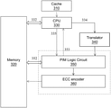
- FIG. 3 is a schematic drawing of a data processing system 300 having a memory implemented with PIM capabilities, in accordance with some embodiments.
- the data processing system 300 includes a memory 320 , a processor 330 (such as a Central Processing Unit), a cache memory 310 , a translator 340 , a PIM enabling logic circuit 350 , and an ECC encoder 360 . While the PIM enabling logic circuit 350 often has registers to support PIM related operations, the PIM enabling logic circuit 350 sometimes include dedicated local memories (such as cache memories) for data storage or microcode storage.
- the data bus 332 is implemented for data transmission between the memory 320 and the processor 330 , and the data bus 352 is implemented for data transmission between the memory 320 and the PIM enabling logic circuit 350 .
- the category of the instruction received is determined by the processor 330 .
- Some of the instructions received by the processor 330 belong to the instruction set of the processor 330 .
- Some of the instructions received by the processor 330 are instructions intended for the PIM enabling logic circuit 350 .
- the digital signal connections 335 and 353 are implemented for data exchanges between the processor 330 and the PIM enabling logic circuit 350 .
- the digital signal connection 334 is implemented to transmit data from the processor 330 to the translator 340 .
- the PIM enabling logic circuit 350 and the ECC encoder 360 are implemented as a part of the memory 320 .
- the translator 340 is also implemented as a part of the memory 320 . Adding the PIM enabling logic circuit 350 and the ECC encoder 360 to the memory 320 enables the memory 320 to perform various supported operations on ECC encoded data in the memory 320 directly, with reduced operation working load on the processor 330 (such as a Central Processing Unit).
- the memory 320 which includes the PIM enabling logic circuit 350 and the ECC encoder 360 as internal circuits, are implemented on a single memory chip. In some embodiments, the memory 320 , which includes the PIM enabling logic circuit 350 and the ECC encoder 360 as internal circuits, are provided to IC designers and/or manufacturers as one or more Intellectual Property files (such as layout files in GDSII format or circuit files in Verilog/VHDL format).
- Intellectual Property files such as layout files in GDSII format or circuit files in Verilog/VHDL format.
- FIG. 4 is a classification diagram of the instructions received by the processor 330 , in accordance with some embodiments.
- the instructions received by the processor 330 are classified into three categories.
- the first category 435 encompasses memory-specific instructions intended specifically for being executed in the PIM enabling logic circuit 350 .
- the second category 425 encompasses memory PIM compatible instructions in a first portion of the instruction set 420 of the processor 330 , intended for being translated into PIM instructions for the PIM enabling logic circuit 350 .
- the third category 428 encompasses memory PIM compatible instructions in a second portion of the instruction set 420 of the processor 330 , intended for being executed in the processor 330 as native instructions.
- each instruction in the first category 435 and the second category 425 has a corresponding PIM instruction of the PIM ISA for the PIM enabling logic circuit 350 .
- Each instruction in the instruction set 420 of the CPU ISA for the processor 330 belongs either to the second category 425 or to the third category 428 .
- the selected instruction belongs to the second category 425 .
- the bitwise operator XOR for the processor 330 is classified as belonging to the second category 425 .
- FIG. 5 is a flow chart of a method 500 of data manipulation for a memory device, in accordance with some embodiments.
- an instruction is received by a first processor, e.g., processor 330 ( FIG. 3 ).
- the instructions received by the processor 330 are fetched from the cache memory 310 .
- the category of the instruction received is determined by the first processor. In some embodiments, as shown in FIG.
- each of the instructions received by the processor 330 belongs to one of the three categories: the first category 435 of the memory-specific instructions, the second category 425 of the memory PIM compatible instructions, or the third category 428 of PIM-unassigned native instructions of the processor 330 .
- the process flow proceeds to operation 535 , but if the instruction does not belong to the category of memory-specific instructions, the process flow proceeds to operation 540 .
- one or more memory-specific instructions are executed in the PIM enabling logic circuit, e.g., PIM logic circuit 350 ( FIG. 3 ).
- the instructions received by the processor 330 are forwarded to the PIM enabling logic circuit 350 though the digital signal connection 335 , and one or more memory-specific instructions are executed in the PIM enabling logic circuit 350 .
- the data bus 352 enables data to be fetched from the memory 320 to the PIM enabling logic circuit 350 and enables data to be sent to the memory 320 from the PIM enabling logic circuit 350 .
- operation 540 which is in the “NO” branch from the operation 530 in FIG. 5 , if the instruction received belongs to a category of memory PIM compatible instructions (such as the second category 425 in FIG. 4 ), the process flow proceeds to operation 545 , but if the instruction received does not belong to a category of memory PIM compatible instructions, the process flow proceeds to operation 560 .
- a category of memory PIM compatible instructions such as the second category 425 in FIG. 4
- the instruction received is executed in the first processor as a native instruction of the first processor.
- the instruction received is executed in the processor 330 .
- the instruction received is an instruction in the instruction set 420 of the CPU ISA as shown in FIG. 4 .
- An instruction in the instruction set 420 of the CPU ISA for the processor 330 belongs either to the second category 425 or to the third category 428 .
- the instruction received does not belong to the second category 425 of memory PIM compatible instructions.
- the instruction received belongs to the third category 428 , which is a category of memory PIM-unassigned native instructions of the processor 330 .
- the data bus 332 enables data to be fetched from the memory 320 to the processor 330 and enables data to be sent to the memory 320 from the processor 330 .
- operation 545 which is in the “YES” branch from the operation 540 in FIG. 5 , if the instruction received is assigned to the PIM enabling logic circuit for further processing, the process flow proceeds to operation 550 , but if the instruction received is not assigned to the PIM enabling logic circuit for further processing, the process flow proceeds to operation 560 .
- the determination of whether an instruction needs to be assigned to the PIM enabling logic circuit is static, and the assignment does not depend upon the working load of the first processor.
- the determination of whether an instruction needs to be assigned to the PIM enabling logic circuit is dynamic, and the assignment depends upon the working load balance between the first processor and the PIM enabling logic circuit.
- an ECC-Space operation corresponding to the instruction received is selected and the ECC-Space operation executed in a PIM enabling logic circuit.
- the instruction received is a memory PIM compatible instruction in the second category 425
- the instruction received is sent to the translator 340 through the digital signal connection 334 .
- An ECC-Space operation corresponding to the instruction received is selected by the translator 340 based on the instruction received from the processor 330 .
- the ECC-Space operation selected is executed in the PIM enabling logic circuit 350 .
- the data bus 352 enables data to be fetched from the memory 320 to the PIM enabling logic circuit 350 and enables data to be sent to the memory 320 from the PIM enabling logic circuit 350 .
- an ECC-Space operation corresponding to the instruction received is selected by the translator 340 based on a lookup table, and the ECC-Space operation is transmitted to the PIM enabling logic circuit 350 .
- an ECC-Space operation selected is represented by a proxy in the form of a truncated ECC-Space operation, and the truncated ECC-Space operation corresponding to the instruction received is transmitted to the PIM enabling logic circuit 350 .
- the operations 535 , 550 , and 560 are category dependent operations, because the category of the instruction received determines which one of the operations 535 , 550 , and 560 is carried out (also referred to as being executed). If the category of the instruction received is the category of memory-specific instructions (such as the first category 435 in FIG. 4 ), the operation 535 is executed accordingly. If the category of the instruction received is the category of memory PIM compatible instructions (such as the second category 425 in FIG. 4 ), the operation 550 is executed accordingly. If the category of the instruction received is the category of PIM-unassigned native instructions (such as the third category 428 in FIG. 4 ), the operation 560 is executed accordingly.
- the instruction received corresponds to a two operands operation * for the processor 330 , and the two operands operation is operative to transform a first data and a second data into a third data.
- the two operands operation * is represented by an opcode for the processor 330 .
- the ECC-Space operation ⁇ tilde over (*) ⁇ corresponding to the two operands operation * is represented by an opcode for the PIM enabling logic circuit 350 .
- the ECC-Space operation ⁇ tilde over (*) ⁇ is operative to transform an ECC encoded first data and an ECC encoded second data into a third data.
- the truncated ECC-Space operation * corresponding to the two operands operation * is represented by an opcode for the PIM enabling logic circuit 350 .
- the truncated ECC-Space operation *′ is operative to transform an ECC encoded first data and an ECC encoded second data into an ECC encoded third data.
- the opcode representing the two operands operation * is transmitted to the translator 340 from the processor 330 through the digital signal connection 334 .
- the opcode representing the two operands operation * is received by the translator 340 , based on a lookup table in the translator 340 , the opcode representing the ECC-Space operation ⁇ tilde over (*) ⁇ corresponding to the two operands operation * is transmitted to the PIM enabling logic circuit 350 from the translator 340 . Then, the ECC-Space operation ⁇ tilde over (*) ⁇ is executed in the PIM enabling logic circuit 350 .
- the ECC encoded first data ECC(x) and the ECC encoded second data ECC(y) are fetched from the memory 320 to the PIM enabling logic circuit 350 through the data bus 352 .
- the opcode representing the two operands operation * is received by the translator 340 , based on a lookup table in the translator 340 , the opcode representing the truncated ECC-Space operation *′ corresponding to the two operands operation * is transmitted to the PIM enabling logic circuit 350 from the translator 340 . Then, the truncated ECC-Space operation *′ is executed in the PIM enabling logic circuit 350 . During the execution of the truncated ECC-Space operation *′, the ECC encoded first data ECC(x) and the ECC encoded second data ECC(y) are fetched from the memory 320 to the PIM enabling logic circuit 350 through the data bus 352 .
- the ECC encoded third data ECC(z) is generated from the third data z by the ECC encoder 360 based on the ECC encoding processes implemented for the memory device.
- the ECC encoded third data ECC(z) is transmitted to the memory 320 .
- the ECC-Space operation ⁇ tilde over (*) ⁇ or the truncated ECC-Space operation *′ is implemented as logic circuits in the PIM enabling logic circuit 350 .
- the logic circuits for implementing the ECC-Space operation ⁇ tilde over (*) ⁇ or the truncated ECC-Space operation *′ are determined based on the two operands operation * and the ECC algorithm for encoding the data in the memory 320 .
- the PIM enabling logic circuit 350 includes a PIM enabling processor, in which the ECC-Space operation ⁇ tilde over (*) ⁇ or the truncated ECC-Space operation *′ is implemented as microprograms comprising instructions from the instruction set of the PIM enabling processor.
- the microprograms for implementing the ECC-Space operation ⁇ tilde over (*) ⁇ or the truncated ECC-Space operation *′ are determined based on the two operands operation * and the ECC algorithm for encoding the data in the memory 320 .
- the PIM enabling logic circuit 350 and the ECC encoder 360 are combined with the memory 320 to form a stand-alone memory system.
- the stand-alone memory system provides the flexibility of combining with various kinds of CPU 330 , various kinds of translator 340 , and various kinds of cache memory 310 , for performing data manipulations on ECC encoded data in the memory.
- one or both of the PIM enabling logic circuit 350 and the ECC encoder 360 are part of the memory 320 .
- the implementations of the truncated ECC-Space operation *′ are determined based on the mathematic relationships connecting the truncated ECC-Space operation *′ to the two operands operation * and the ECC algorithm for encoding the data in the memory 320 .
- the Hamming ECC algorithm when the Hamming ECC algorithm is selected as the ECC algorithm for encoding the data in the memory 320 , the mathematic relationships connecting the truncated ECC-Space operation *′ to the two operands operation * and the Hamming ECC algorithm are explained in the following.
- ECC( ⁇ right arrow over (z) ⁇ ) [z′ 1 , z′ 2 , z′ 3 , . . . z′ m ] T .
- ECC( ⁇ right arrow over (x) ⁇ ), ECC( ⁇ right arrow over (y) ⁇ ), and ECC( ⁇ right arrow over (z) ⁇ ) is in the Euclidian space 12 ′ and also represents an ECC coded data
- the Euclidian space 12 ′ in the present disclosure is defined as an ECC-Space.
- each of the ECC encoded data in the memory 320 is the (7, 4) Hamming code
- the generator matrix for the (7, 4) Hamming code is,
- ECC( ⁇ right arrow over (z) ⁇ ) ⁇ right arrow over (z) ⁇
- the vector ECC( ⁇ right arrow over (z) ⁇ ) can also be obtained from the vectors ECC( ⁇ right arrow over (x) ⁇ ) and ECC( ⁇ right arrow over (y) ⁇ ).
- ECC-Space operation *′ can be determined based on the two operands operation * for the first processor using the (7, 4) Hamming coding algorithm
- the vector ⁇ right arrow over (z) ⁇ is obtained from the vectors ECC( ⁇ right arrow over (x) ⁇ ) and ECC( ⁇ right arrow over (y) ⁇ ) based on the following equations:
- z 1 ⁇ [ ( x 1 ′ + x 2 ′ + x 3 ′ + x 5 ′ ) ⁇ ( x 1 ′ + x 2 ′ + x 4 ′ + x 6 ′ ) ⁇ ( x 1 ′ + x 3 ′ + x 4 ′ + x 7 ′ ) ⁇ x 1 ′ ] * [ ( y 1 ′ + y 2 ′ + y 3 ′ + y 5 ′ ) ⁇ ( y 1 ′ + y 2 ′ + y 4 ′ + y 6 ′ ) ⁇ ( y 1 ′ + y 3 ′ + y 4 ′ + y 7 ′ ) ⁇ y 1 ′ ]
- ⁇ z 2 ⁇ [ ( x 1 ′ + x 2 ′ + x 3 ′ + x 5 ′ ) ⁇ ( x 1 ′ + x 2 ′ + x 4 ′ + x 6 ′ )
- bitwise operator * is one of the bitwise logic operations, such as, the bitwise AND, the bitwise OR, the bitwise NOR, the bitwise XOR, or the bitwise NAND.
- the notations ECC( ⁇ right arrow over (x) ⁇ ′) [x′ 1 , x′ 2 , x′ 3 , . . . x′ m ] T and ECC( ⁇ right arrow over (y) ⁇ ′), [y′ 1 , y′ 2 , y′ 3 , . . .
- the operation *′ obtained based on the above equations for expressing the components z 1 , z 2 , z 3 , and z 4 is implemented as logic circuits in the PIM enabling logic circuit 350 .
- the operation *′ obtained based on the above equations is implemented as microprograms in the PIM enabling logic circuit 350 .
- the ECC-Space operation ⁇ tilde over (*) ⁇ is then implemented as logic circuits in the PIM enabling logic circuit 350 .
- the ECC-Space operation ⁇ tilde over (*) ⁇ is then implemented as microprograms in the PIM enabling logic circuit 350 .
- the PIM enabling logic circuit 350 After the ECC-Space operation ⁇ tilde over (*) ⁇ is executed in the PIM enabling logic circuit 350 using the ECC encoded first data ECC(x) as a first operand and the ECC coded second data ECC(y) as a second operand, the PIM enabling logic circuit 350 generates an ECC encoded output data.
- the ECC encoded output data is identical to a result of coding the third data z with the ECC algorithm, if the third data z is generated by executing the native operation * in the processor 330 using the first data x as a first operand and the second data y as a second operand.
- the ECC algorithm used for determining and implementing the operation *′ or the operation ⁇ tilde over (*) ⁇ is based on the Binary Golay codes, the Bose-Chaudhuri-Hocquenghem (BCH) codes, or the Low-density parity-check (LDPC) codes.
- BCH Bose-Chaudhuri-Hocquenghem
- LDPC Low-density parity-check
- the truncated ECC-Space operation *′ or the ECC-Space operation ⁇ tilde over (*) ⁇ is implemented based on above described procedures for a set of bitwise operators which are functionally complete. Base on the functionally complete set of bitwise operators, other ECC-Space operations, such as word-wise logic operations or word-wise arithmetic operations, are implemented to support more complicated operations.
- word-wise arithmetic operations such as ADD or MULTIPLY are implemented in the PIM enabling logic circuit 350 as logic circuits or implemented as microprograms in a processor in the PIM enabling logic circuit 350 that supports the basic ECC-Space bit-wise logic operations.
- An aspect of the present disclosure relates to a method.
- the method includes transmitting an ECC encoded first data and an ECC encoded second data from a memory to a logic circuit.
- the ECC encoded first data is identical to a result of encoding a first data with an ECC algorithm and the ECC encoded second data is identical to a result of encoding a second data with the ECC algorithm.
- the method also includes generating an ECC encoded output data by executing an ECC-Space operation using the ECC encoded first data as a first operand and the ECC encoded second data as a second operand.
- the ECC-Space operation is translated from a two operands operation of a first processor and the two operands operation is operative to transform the first data and the second data into a third data.
- the ECC encoded output data is identical to a result of encoding the third data with the ECC algorithm if the third data is encoded with the ECC algorithm.
- Another aspect of the present disclosure relate to a method of processing data in a memory device that supports processing-in-memory (“PIM”) operations.
- the method includes determining a category of an instruction received by a first processor, and processing one or more category-dependent operations based on the category determined.
- the category dependent operations includes, if the category of the instruction received is a category of memory PIM compatible instructions, selecting an ECC-Space operation corresponding to the instruction received and executing the ECC-Space operation in a logic circuit, and if the category of the instruction received is a category of PIM-unassigned native instructions of the first processor, executing the instruction in the first processor.
- Still another aspect of the present disclosure relate to a device.
- the device includes a memory operative to store an ECC encoded first data and an ECC encoded second data, and a logic circuit, connecting with the memory through a first data bus, and configured to execute an ECC-Space operation operative to generate an ECC encoded output data from the ECC encoded first data and the ECC encoded second data.
- the ECC encoded first data is identical to a result of encoding a first data with an ECC algorithm and the ECC encoded second data is identical to a result of encoding a second data with the ECC algorithm.
- the ECC-Space operation is translated from a two operands operation that is operative to transform the first data and the second data into a third data. If the ECC encoded output data is decoded with the ECC algorithm, a result of decoding the ECC encoded output data with the ECC algorithm is identical to the third data.
Abstract
Description
{right arrow over (x)}=[x 1 ,x 2 ,x 3 ,x 4]T,
{right arrow over (y)}=[y 1 ,y 2 ,y 3 ,y 4]T,
{right arrow over (z)}=[z 1 ,z 2 ,z 3 ,z 4]T.
Furthermore, the ECC encoded first data ECC(x), the ECC encoded second data ECC(y), and the ECC encoded third data ECC(z) are correspondingly represented by the column vectors ECC(0.0, ECC(y), and ECC({right arrow over (z)}), which are expressed as the mathematical relationships in the following:
ECC({right arrow over (x)})=[x′ 1 ,x′ 2 ,x′ 3 ,x′ 4 ,x′ 5 ,x′ 6 ,x′ 7]T,
ECC({right arrow over (y)})=[y′ 1 ,y′ 2 ,y′ 3 ,y′ 4 ,y′ 5 ,y′ 6 ,y′ 7]T,
ECC({right arrow over (z)})=[z′ 1 ,z′ 2 ,z′ 3 ,z′ 4 ,z′ 5 ,z′ 6 ,z′ 7]T.
When the generator matrix
ECC({right arrow over (z)})=[z 1 ,z 2 ,z 3 ,z 4 ,z 1 +z 2 +z 3 ,z 1 +z 2 +z 4 ,z 1 +z 3 +z 4]T
With the (7, 4) Hamming code, when the ECC encoded third data ECC(z) has no bit-flip errors, z′1=z1, z′2=z2, z3=z′3, z′4=z4; furthermore, z′5=z1+z2+z3, z′6=z1+z2+z4, and z′7=z1+z3+z4. Because ECC({right arrow over (z)})=
{right arrow over (z)}=ECC({right arrow over (x)})*′ECC({right arrow over (y)}),
then the vector ECC({right arrow over (z)}) can also be obtained from the vectors ECC({right arrow over (x)}) and ECC({right arrow over (y)}). That is, if the truncated ECC-Space operation *′ can be determined based on the two operands operation * for the first processor using the (7, 4) Hamming coding algorithm, then the ECC-Space operation {tilde over (*)} can also be determined such that
ECC({right arrow over (z)})=ECC({right arrow over (x)}){tilde over (*)}ECC({right arrow over (y)}).
{right arrow over (z)}=[z 1 ,z 2 ,z 3 ,z 4]T=ECC({right arrow over (x)})*′ECC({right arrow over (y)}),
the truncated ECC-Space operation *′ is obtained. In some embodiments, the operation *′ obtained based on the above equations for expressing the components z1, z2, z3, and z4 is implemented as logic circuits in the PIM enabling
ECC({right arrow over (z)})=[z 1 ,z 2 ,z 3 ,z 4 ,z 1 +z 2 +z 3 ,z 1 +z 2 +z 4 ,z 1 +z 3 ±z 4]T=
ECC({right arrow over (x)}){tilde over (*)}ECC({right arrow over (y)}),
the ECC-Space operation {tilde over (*)} is obtained. In some embodiments, after the operation {tilde over (*)} is determined based on the equations for expressing z1, z2, z3, and z4 in terms of ECC(x) and ECC({right arrow over (y)}), the ECC-Space operation {tilde over (*)} is then implemented as logic circuits in the PIM enabling
Claims (20)
Priority Applications (4)
| Application Number | Priority Date | Filing Date | Title |
|---|---|---|---|
| US17/143,717 US11237907B2 (en) | 2020-05-29 | 2021-01-07 | Processing-in-memory instruction set with homomorphic error correction |
| TW110118542A TW202145012A (en) | 2020-05-29 | 2021-05-21 | Method and apparatus for processing data in memory device |
| CN202110566937.5A CN113220499A (en) | 2020-05-29 | 2021-05-24 | Data processing method and device of memory device |
| US17/649,457 US11687412B2 (en) | 2020-05-29 | 2022-01-31 | Processing-in-memory instruction set with homomorphic error correction |
Applications Claiming Priority (2)
| Application Number | Priority Date | Filing Date | Title |
|---|---|---|---|
| US202063031917P | 2020-05-29 | 2020-05-29 | |
| US17/143,717 US11237907B2 (en) | 2020-05-29 | 2021-01-07 | Processing-in-memory instruction set with homomorphic error correction |
Related Child Applications (1)
| Application Number | Title | Priority Date | Filing Date |
|---|---|---|---|
| US17/649,457 Continuation US11687412B2 (en) | 2020-05-29 | 2022-01-31 | Processing-in-memory instruction set with homomorphic error correction |
Publications (2)
| Publication Number | Publication Date |
|---|---|
| US20210374002A1 US20210374002A1 (en) | 2021-12-02 |
| US11237907B2 true US11237907B2 (en) | 2022-02-01 |
Family
ID=77098204
Family Applications (2)
| Application Number | Title | Priority Date | Filing Date |
|---|---|---|---|
| US17/143,717 Active US11237907B2 (en) | 2020-05-29 | 2021-01-07 | Processing-in-memory instruction set with homomorphic error correction |
| US17/649,457 Active US11687412B2 (en) | 2020-05-29 | 2022-01-31 | Processing-in-memory instruction set with homomorphic error correction |
Family Applications After (1)
| Application Number | Title | Priority Date | Filing Date |
|---|---|---|---|
| US17/649,457 Active US11687412B2 (en) | 2020-05-29 | 2022-01-31 | Processing-in-memory instruction set with homomorphic error correction |
Country Status (3)
| Country | Link |
|---|---|
| US (2) | US11237907B2 (en) |
| CN (1) | CN113220499A (en) |
| TW (1) | TW202145012A (en) |
Families Citing this family (5)
| Publication number | Priority date | Publication date | Assignee | Title |
|---|---|---|---|---|
| US11586500B2 (en) * | 2019-09-23 | 2023-02-21 | SK Hynix Inc. | Processing-in-memory (PIM) devices |
| KR20210034999A (en) | 2019-09-23 | 2021-03-31 | 에스케이하이닉스 주식회사 | AIM device and method of multiplying/accumulation in the AIM device |
| US11586494B2 (en) | 2019-09-23 | 2023-02-21 | SK Hynix Inc. | Processing-in-memory (PIM) devices |
| KR20220067961A (en) * | 2020-11-18 | 2022-05-25 | 삼성전자주식회사 | Processing-in-memory and method for outputting instruction using processing-in-memory |
| US11734114B2 (en) * | 2020-12-09 | 2023-08-22 | Advanced Micro Devices, Inc. | Programmable error correction code encoding and decoding logic |
Citations (10)
| Publication number | Priority date | Publication date | Assignee | Title |
|---|---|---|---|---|
| US5689727A (en) * | 1994-09-08 | 1997-11-18 | Western Digital Corporation | Disk drive with pipelined embedded ECC/EDC controller which provides parallel operand fetching and instruction execution |
| US20100269016A1 (en) * | 2009-04-16 | 2010-10-21 | Micron Technology, Inc. | Multiple-level memory cells and error detection |
| US20130139028A1 (en) * | 2011-11-28 | 2013-05-30 | Texas Instruments Incorporated | Extended Bidirectional Hamming Code for Double-Error Correction and Triple-Error Detection |
| US20150280748A1 (en) * | 2014-03-26 | 2015-10-01 | Alexander Gendler | Double consecutive error correction |
| US20150363263A1 (en) * | 2014-06-12 | 2015-12-17 | HGST Netherlands B.V. | ECC Encoder Using Partial-Parity Feedback |
| US20170083237A1 (en) * | 2015-09-23 | 2017-03-23 | Hanan Potash | Computing device with frames/bins structure, mentor layer and plural operand processing |
| US20190102254A1 (en) * | 2017-09-29 | 2019-04-04 | Nvidia Corporation | Securing against errors in an error correcting code (ecc) implemented in an automotive system |
| US20200097360A1 (en) * | 2018-09-21 | 2020-03-26 | Taiwan Semiconductor Manufacturing Company Ltd. | System and method of reducing logic for multi-bit error correcting codes |
| US20200293452A1 (en) * | 2019-03-11 | 2020-09-17 | Samsung Electronics Co,Ltd | Memory device and method including circular instruction memory queue |
| US11029958B1 (en) * | 2019-12-28 | 2021-06-08 | Intel Corporation | Apparatuses, methods, and systems for configurable operand size operations in an operation configurable spatial accelerator |
Family Cites Families (3)
| Publication number | Priority date | Publication date | Assignee | Title |
|---|---|---|---|---|
| US11164033B2 (en) * | 2015-05-29 | 2021-11-02 | Micron Technology, Inc. | Histogram creation process for memory devices |
| US10606587B2 (en) * | 2016-08-24 | 2020-03-31 | Micron Technology, Inc. | Apparatus and methods related to microcode instructions indicating instruction types |
| CN111679785A (en) * | 2019-03-11 | 2020-09-18 | 三星电子株式会社 | Memory device for processing operation, operating method thereof and data processing system |
-
2021
- 2021-01-07 US US17/143,717 patent/US11237907B2/en active Active
- 2021-05-21 TW TW110118542A patent/TW202145012A/en unknown
- 2021-05-24 CN CN202110566937.5A patent/CN113220499A/en active Pending
-
2022
- 2022-01-31 US US17/649,457 patent/US11687412B2/en active Active
Patent Citations (10)
| Publication number | Priority date | Publication date | Assignee | Title |
|---|---|---|---|---|
| US5689727A (en) * | 1994-09-08 | 1997-11-18 | Western Digital Corporation | Disk drive with pipelined embedded ECC/EDC controller which provides parallel operand fetching and instruction execution |
| US20100269016A1 (en) * | 2009-04-16 | 2010-10-21 | Micron Technology, Inc. | Multiple-level memory cells and error detection |
| US20130139028A1 (en) * | 2011-11-28 | 2013-05-30 | Texas Instruments Incorporated | Extended Bidirectional Hamming Code for Double-Error Correction and Triple-Error Detection |
| US20150280748A1 (en) * | 2014-03-26 | 2015-10-01 | Alexander Gendler | Double consecutive error correction |
| US20150363263A1 (en) * | 2014-06-12 | 2015-12-17 | HGST Netherlands B.V. | ECC Encoder Using Partial-Parity Feedback |
| US20170083237A1 (en) * | 2015-09-23 | 2017-03-23 | Hanan Potash | Computing device with frames/bins structure, mentor layer and plural operand processing |
| US20190102254A1 (en) * | 2017-09-29 | 2019-04-04 | Nvidia Corporation | Securing against errors in an error correcting code (ecc) implemented in an automotive system |
| US20200097360A1 (en) * | 2018-09-21 | 2020-03-26 | Taiwan Semiconductor Manufacturing Company Ltd. | System and method of reducing logic for multi-bit error correcting codes |
| US20200293452A1 (en) * | 2019-03-11 | 2020-09-17 | Samsung Electronics Co,Ltd | Memory device and method including circular instruction memory queue |
| US11029958B1 (en) * | 2019-12-28 | 2021-06-08 | Intel Corporation | Apparatuses, methods, and systems for configurable operand size operations in an operation configurable spatial accelerator |
Non-Patent Citations (1)
| Title |
|---|
| Yang X, Hou Y, He H. A Processing-in-Memory Architecture Programming Paradigm for Wireless Internet-of-Things Applications. Sensors (Basel). 2019;19(1):140. Published Jan. 3, 2019. doi:10.3390/s19010140 (Year: 2019). * |
Also Published As
| Publication number | Publication date |
|---|---|
| US11687412B2 (en) | 2023-06-27 |
| TW202145012A (en) | 2021-12-01 |
| CN113220499A (en) | 2021-08-06 |
| US20210374002A1 (en) | 2021-12-02 |
| US20220166445A1 (en) | 2022-05-26 |
Similar Documents
| Publication | Publication Date | Title |
|---|---|---|
| US11237907B2 (en) | Processing-in-memory instruction set with homomorphic error correction | |
| US9015452B2 (en) | Vector math instruction execution by DSP processor approximating division and complex number magnitude | |
| US9075739B2 (en) | Storage device | |
| TWI643124B (en) | Apparatus, method, and system for providing information processing | |
| KR20090028507A (en) | Non-volatile memory error correction system and method | |
| JP2006244259A (en) | In-byte plural spotty byte error correction/detection method and device limiting error byte number | |
| US20040117688A1 (en) | Error correction for flash memory | |
| US9110768B2 (en) | Residue based error detection for integer and floating point execution units | |
| US8700971B2 (en) | Parallel residue arithmetic operation unit and parallel residue arithmetic operating method | |
| CN111192622B (en) | Flash memory controller and coding circuit and decoding circuit therein | |
| US11922133B2 (en) | Processor and method for processing mask data | |
| US3688265A (en) | Error-free decoding for failure-tolerant memories | |
| Cho et al. | Efficient software-based encoding and decoding of BCH codes | |
| US11409608B2 (en) | Providing host-based error detection capabilities in a remote execution device | |
| US20040088497A1 (en) | Methods and apparatus for exchanging data using cyclic redundancy check codes | |
| Tam | Single error correction and double error detection | |
| CN110322922B (en) | Apparatus and system for in-band dynamic random access memory error correction coding | |
| US7647368B2 (en) | Data processing apparatus and method for performing data processing operations on floating point data elements | |
| TWI664636B (en) | Error checking and correcting decoder | |
| EP0936537B1 (en) | Cyclic redundancy check in a computer system | |
| US20240146336A1 (en) | Integration of compression algorithms with error correction codes | |
| TW202024907A (en) | Processing of data | |
| Lee et al. | Implementation of parallel BCH encoder employing tree-type systolic array architecture | |
| US20230412190A1 (en) | Encoder and decoder | |
| JPWO2019030860A1 (en) | Method and apparatus for generating redundant bit for error detection |
Legal Events
| Date | Code | Title | Description |
|---|---|---|---|
| AS | Assignment |
Owner name: TAIWAN SEMICONDUCTOR MANUFACTURING COMPANY, LTD., TAIWAN Free format text: ASSIGNMENT OF ASSIGNORS INTEREST;ASSIGNOR:CHIANG, KATHERINE H;REEL/FRAME:054848/0191 Effective date: 20201216 |
|
| FEPP | Fee payment procedure |
Free format text: ENTITY STATUS SET TO UNDISCOUNTED (ORIGINAL EVENT CODE: BIG.); ENTITY STATUS OF PATENT OWNER: LARGE ENTITY |
|
| STPP | Information on status: patent application and granting procedure in general |
Free format text: NOTICE OF ALLOWANCE MAILED -- APPLICATION RECEIVED IN OFFICE OF PUBLICATIONS |
|
| STPP | Information on status: patent application and granting procedure in general |
Free format text: PUBLICATIONS -- ISSUE FEE PAYMENT VERIFIED |
|
| STCF | Information on status: patent grant |
Free format text: PATENTED CASE |