US11233142B2 - Intrinsically tunable and ultra-linear multi-fin MIS-HEMT devices - Google Patents
Intrinsically tunable and ultra-linear multi-fin MIS-HEMT devices Download PDFInfo
- Publication number
- US11233142B2 US11233142B2 US16/759,653 US201816759653A US11233142B2 US 11233142 B2 US11233142 B2 US 11233142B2 US 201816759653 A US201816759653 A US 201816759653A US 11233142 B2 US11233142 B2 US 11233142B2
- Authority
- US
- United States
- Prior art keywords
- fins
- fin
- mis
- hemt
- gate
- Prior art date
- Legal status (The legal status is an assumption and is not a legal conclusion. Google has not performed a legal analysis and makes no representation as to the accuracy of the status listed.)
- Active
Links
Images


Classifications
-
- H01L29/7783—
-
- H—ELECTRICITY
- H10—SEMICONDUCTOR DEVICES; ELECTRIC SOLID-STATE DEVICES NOT OTHERWISE PROVIDED FOR
- H10D—INORGANIC ELECTRIC SEMICONDUCTOR DEVICES
- H10D30/00—Field-effect transistors [FET]
- H10D30/40—FETs having zero-dimensional [0D], one-dimensional [1D] or two-dimensional [2D] charge carrier gas channels
- H10D30/47—FETs having zero-dimensional [0D], one-dimensional [1D] or two-dimensional [2D] charge carrier gas channels having two-dimensional [2D] charge carrier gas channels, e.g. nanoribbon FETs or high electron mobility transistors [HEMT]
- H10D30/471—High electron mobility transistors [HEMT] or high hole mobility transistors [HHMT]
- H10D30/473—High electron mobility transistors [HEMT] or high hole mobility transistors [HHMT] having confinement of carriers by multiple heterojunctions, e.g. quantum well HEMT
- H10D30/4732—High electron mobility transistors [HEMT] or high hole mobility transistors [HHMT] having confinement of carriers by multiple heterojunctions, e.g. quantum well HEMT using Group III-V semiconductor material
-
- H01L29/2003—
-
- H01L29/7786—
-
- H01L29/7787—
-
- H01L29/785—
-
- H—ELECTRICITY
- H10—SEMICONDUCTOR DEVICES; ELECTRIC SOLID-STATE DEVICES NOT OTHERWISE PROVIDED FOR
- H10D—INORGANIC ELECTRIC SEMICONDUCTOR DEVICES
- H10D30/00—Field-effect transistors [FET]
- H10D30/40—FETs having zero-dimensional [0D], one-dimensional [1D] or two-dimensional [2D] charge carrier gas channels
- H10D30/47—FETs having zero-dimensional [0D], one-dimensional [1D] or two-dimensional [2D] charge carrier gas channels having two-dimensional [2D] charge carrier gas channels, e.g. nanoribbon FETs or high electron mobility transistors [HEMT]
- H10D30/471—High electron mobility transistors [HEMT] or high hole mobility transistors [HHMT]
- H10D30/475—High electron mobility transistors [HEMT] or high hole mobility transistors [HHMT] having wider bandgap layer formed on top of lower bandgap active layer, e.g. undoped barrier HEMTs such as i-AlGaN/GaN HEMTs
- H10D30/4755—High electron mobility transistors [HEMT] or high hole mobility transistors [HHMT] having wider bandgap layer formed on top of lower bandgap active layer, e.g. undoped barrier HEMTs such as i-AlGaN/GaN HEMTs having wide bandgap charge-carrier supplying layers, e.g. modulation doped HEMTs such as n-AlGaAs/GaAs HEMTs
-
- H—ELECTRICITY
- H10—SEMICONDUCTOR DEVICES; ELECTRIC SOLID-STATE DEVICES NOT OTHERWISE PROVIDED FOR
- H10D—INORGANIC ELECTRIC SEMICONDUCTOR DEVICES
- H10D30/00—Field-effect transistors [FET]
- H10D30/60—Insulated-gate field-effect transistors [IGFET]
- H10D30/62—Fin field-effect transistors [FinFET]
-
- H—ELECTRICITY
- H10—SEMICONDUCTOR DEVICES; ELECTRIC SOLID-STATE DEVICES NOT OTHERWISE PROVIDED FOR
- H10D—INORGANIC ELECTRIC SEMICONDUCTOR DEVICES
- H10D62/00—Semiconductor bodies, or regions thereof, of devices having potential barriers
- H10D62/10—Shapes, relative sizes or dispositions of the regions of the semiconductor bodies; Shapes of the semiconductor bodies
- H10D62/117—Shapes of semiconductor bodies
-
- H—ELECTRICITY
- H10—SEMICONDUCTOR DEVICES; ELECTRIC SOLID-STATE DEVICES NOT OTHERWISE PROVIDED FOR
- H10D—INORGANIC ELECTRIC SEMICONDUCTOR DEVICES
- H10D62/00—Semiconductor bodies, or regions thereof, of devices having potential barriers
- H10D62/80—Semiconductor bodies, or regions thereof, of devices having potential barriers characterised by the materials
- H10D62/85—Semiconductor bodies, or regions thereof, of devices having potential barriers characterised by the materials being Group III-V materials, e.g. GaAs
- H10D62/8503—Nitride Group III-V materials, e.g. AlN or GaN
Definitions
- a field of the invention is semiconductor devices and semiconductor device fabrication.
- the invention particular concerns metal insulator semiconductor high electron mobility transistor (MIS-HEMT) devices.
- MIS-HEMT metal insulator semiconductor high electron mobility transistor
- Non-linearity is embodied in a decrease of the transistor current gain cut-off frequency, f T , and maximum oscillation frequency, f max , with an increase in the drain current. Both f T and f max are directly proportional to the transistor's transconductance, g m , which degrades at high drain currents.
- g m degradation is material dependent, and is caused by (1) mobility degradation due to interface roughness in Si devices; (2) real-space transfer of hot electrons into the barrier in GaAs and InGaAs based HEMTs; (3) self-heating effects, (4) scattering with nonequilibrium hot optical phonons, (5) emission of optical phonons, and (6) increase of the dynamic source access resistance in GaN based HEMTs. See, Palacios, T., Raj an, S., Chakraborty, A., Heikman, S., Keller, S., DenBaars, S. P., Mishra, U.
- the derivative superposition technique [Webster, D., Haigh, D., Scott, J., Parker, A., Derivative superposition-a linearisation technique for ultra broadband systems. 1996] and its variations [Kim, T. W., Kim, B., Lee, K., “Highly linear receiver front-end adopting MOSFET transconductance linearization by multiple gated transistors,” IEEE Journal of Solid - State Circuits 2004, 39 (1), 223-229] including the modified derivative superposition technique [Aparin, V., Larson, L. E., Modified derivative superposition method for linearizing FET low-noise amplifiers. IEEE Transactions on Microwave Theory and Techniques 2005, 53 (2), 571-581] has been heavily utilized for linearizing RF circuits.
- V GS bias range through the use of two or more parallel MOSFETs with different widths and gate biases. Similar to the multi-tanh approach, this technique is extrinsic, is costly for layout area, and cannot be extended to mm wave frequencies due to circuit patristics and bandwidth limitations of the impedance matching elements.
- FIG. 7A shows a nanowire or fin configuration with varying widths. The fins are arranged according to the magnitudes of the peaks and/or valleys or g′′m, which is the second derivative of transconductance. This is known as the derivative superposition technique, previously used widely in communication circuits.
- a preferred MIS-HEMT includes a substrate, a buffer layer upon the substrate, and a plurality of multi-layer fins with channel and barrier material.
- the fins have a plurality of widths and are formed upon the buffer layer, gate insulator surrounds the fins and gate metal conformally covers the gate metal.
- the plurality of widths include largest, intermediate and smallest widths, selected to lead to the separate turn-on voltage thresholds for the largest, intermediate and smallest widths of the MIS-HEMT fins to flatten the transconductance g m curve over an operational range of gate source voltage.
- the planar channel comprises a width greater than 1 ⁇ m, and all of the plurality of widths are less than 500 nm.
- the plurality of widths are selected such that the threshold voltages (V T ) and the peak point of transconductance g m of single Fins from the plurality of Fins lift up a decreasing region of transconductance g m at higher V GS in larger Fins of the plurality of fins.
- the source and drain regions are preferably unetched.
- the channel and barrier materials can be Group III-V materials or silicon with different ion-implant doses.
- the plurality of widths are uniformly separated by gate voltages in second derivative of transconductance g m ′′ curves to complement each other for reducing the first derivative of transconductance g m ′ close to zero over the operational range.
- a preferred method of compensating for the first derivative of transconductance, g m , in a MIS-HEMT includes turning on a first Fin in response to a first gate source voltage.
- a second smaller Fin turns on in response to an increased gate voltage.
- a third Fin smaller than the second smaller Fin turns on in response to a larger increased gate voltage, wherein the first, second smaller, and third Fin are sized such that smaller fin devices with quantitatively calculated weights replenish the negative region of the first derivative of transconductance g m to reduce variation of g m over an operational range of gate source voltage.
- the method preferably includes first turning on a planar channel in response to a gate source voltage that is smaller than the first gate source voltage.
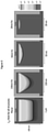
- FIGS. 1A-1C are respective fragmentary cross-sectional, side perspective and top views schematically showing a preferred architecture of combined planar and multi-fin MIS-HEMTs according to the present invention
- FIGS. 2A and 2B are schematic diagrams of a single Fin showing a threshold voltage calculation method for a preferred Fin MIS-HEMT according to the present invention.
- FIGS. 3A and 3B are graphical views showing transistor linearization by the multi-Fin MIS-HEMTs according to the present invention.
- FIG. 4 is the process flow for a preferred fabrication method according to the present invention.
- FIG. 5 shows Silvaco Atlas simulations for the electron density in the cross-section of a planar strip (1 ⁇ m wide) and different Fin widths
- FIG. 6 Line cut of carrier concentration 1 nm below AlGaN barrier for planar and Fin structures
- FIGS. 7A-7F illustrates measured characteristics of a conventional planar device ( FIGS. 7A, 7C, and 7E ) and the linearization provided by the invention ( FIGS. 7B, 7D, and 7F )
- FIG. 8 are g′′ m -V G characteristics of experimental fabricated devices with a planar and different fin widths
- FIG. 9 are g′m-V G characteristics of fabricated devices with a planar and different fin widths and synthesized devices with reduced ⁇ g m ;
- FIG. 10 includes data showing an effect of factor F on ⁇ g m ;
- FIG. 11 is plot of the number of transistors at each threshold voltage
- FIG. 12 is a top-view SEM image of a fabricated multi-fin MIS-HEMT device
- FIGS. 13A 13 D are data plots of device characteristics of a preferred embodiment multi-fin MIS-HEMT.
- FIG. 14 includes a summary of g m ′ at different V G , illustrations present methods of linearization of g m , and defining weights;
- FIGS. 15A-15C are respective fragmentary cross-sectional, side perspective and top views schematically showing a preferred architecture of a multi-fin MIS-HEMT according to the present invention.
- FIGS. 16A-16C are respective fragmentary cross-sectional, side perspective and top views schematically showing a planar MIS-HEMT that is combined with multi-fin FETs according to the present invention.
- FIG. 17 is data plot of threshold voltages (V T ) as a function of fin widths (W Fin ).
- a preferred transistor device architecture provides a capability of intrinsically tunable ultra-wide band linearity.
- Preferred embodiments overcome limitations of the prior approaches in the background by providing devices that permit tuning of the threshold voltage and synthesizing the linearity of transistors using parallel channels that are formed on the surface of the substrate with consistent and controllable gate-to-channel capacitance, and that provide a larger degree of flexibility in material selection such as low work function metal electrodes to push the linearity to voltages that conventional HEMT-based devices cannot achieve.
- Preferred devices use a plurality of Fin structures and/or combine a planar portion with Fin structures to compensate for the first derivative of transconductance, g m .
- Preferred devices enable linearization with a planar channel and multiple Fin channels whose threshold voltage can be individually tuned by width of the Fin-channel, W Fin .
- V GS ⁇ V Tn an is the number of channels for a family of Fins, n, with width W Fin-n , and threshold voltage, V Tn , where V Tn >V Tn ⁇ 1 . Therefore, two simple “engineering knobs” are present in the current device architecture to control the device linearity: W Fin which controls the shift in the threshold voltage, V T , and the amplitude ⁇ n which controls the current output beyond a V T point.
- a planar channel device having a more negative V T than any fin devices broadens the flat g m region much further meaning a more intrinsically linear transistor.
- g m ′ of planar device is negative after V G of ⁇ 4 V, which provides a room that can be replenished by fin devices with higher V T , to make a preferred device have a very broad flat g m region.
- Preferred embodiments achieve an objective of intrinsically tunable high linearity GaN multi-Fin MIS-HEMT devices that can deliver wideband linearity at low DC bias with potential to exceed OIP3/PDC of 1000.
- the intrinsic device characteristics as a function of gate-source voltage in preferred embodiment devices can be controllably synthesized in order to provide the desired linearity, along with high f t , f max and low noise performance.
- Preferred MIS Fin HEMTs provide linear transfer characteristics, through the synthesis of IDS currents from Fin HEMTs that turn on sequentially from large to small and therefore eliminate the usually reduced slope of IDS as a function of Vgs when Vgs increases beyond the ‘linear regime’.
- the transconductance of the device usually decreases rapidly with gate voltages above V T , but preferred devices provide a flat transconductance which leads to a constant gain, large bandwidth, and lower jitter.
- Preferred HEMTs provide a large ⁇ V GS over which the device is linear. The large range is dependent on the number of families of FinFETs that can be integrated into the device. There are also limitations on how much the threshold voltage can be tuned for a particular device that depend upon with (1) size and (2) metal work function.
- HEMTs of preferred embodiments can provide linearity over a large ⁇ V GS up to 10 V, as indicated by simulations. A largest range reported in literature known to the inventors is half or less than half of the 10V range, e.g. only from about 4.5 to 5V, which can also be lower depending upon size and metal work function, and most ranges are far less than that in reported and commercial devices.
- GaN was selected to demonstrate the present device architecture because of its well-known superior physical properties of high electron mobility and saturation velocity, high sheet carrier density and high breakdown fields. These properties make GaN a preferred choice to meet the goals of high linearity and high-power mm wave devices when used with the present architecture.
- GaN material is also a preferred material choice for scalable and economical production of high linearity transmitters.
- the present HEMT device architecture can work for any amplifier material system, including GaAs, InP, InGaAs, InGaN and others.
- transistor channel materials are remotely doped and there is less leverage on the threshold voltage control except for dramatic changes in the device gate capacitance, such as in FinFETs or nanowire FETs, to achieve tunable threshold voltages and therefore linear devices.
- the concept can also be applied to junction-less transistors including Si. Additionally, for Si, an adjustment of the threshold-voltage can be made by implanting the surface of the channel under the gate. As such, different ion-implant doses in parallel channels in a single Si device can achieve linear device characteristics but cannot offer the gain and speed of that for III-V materials.
- FIGS. 1A-1C illustrate an example embodiment combined planar and multi-Fin MIS-HEMTs semiconductor device architecture in an example AlGaN/GaN material, which provides for intrinsically tunable ultra linear millimeter wave devices.
- the basic structure includes a substrate 100 , a buffer 110 , AlGaN/GaN multi-fin layers including a planar region 120 - n , 130 - n having fin to fin distances 104 , gate insulator 140 - n and gate metal 150 .
- the multi-Fin MIS-HEMT includes gate metal 150 and gate insulator 140 - n , e.g.
- Al 2 O 3 , HfO 2 , etc. covering multiple AlGaN/GaN fins 130 - n , 120 - n , sitting on top of the GaN buffer layer 110 atop a substrate 100 , e.g. Si, SiC, sapphire, and GaN.
- the AlGaN/GaN fins 130 - n , 120 - n have a width of 40 nm-1000 nm, and a height of 30 nm ⁇ 1 ⁇ m.
- Narrower fins can provide broader V T range as long as making narrower fin is physically possible. Height should be higher than a barrier layer thickness, because gate metal should cover the sidewall of 2DEG.
- the width of channel 105 can define the structure as a fin or a planar, and we define a planar MIS-HEMT when the width 105 is at least 1 ⁇ m, and preferably 1 ⁇ m to 100 ⁇ m, or a few hundred ⁇ m. We also define a fin MIS-HEMT when the width 105 is 500 nm or less, and preferably 40-500 nm.
- the width of planar region 105 can vary from one to few hundred micrometers depending on the actual device design with respect to a desired total drain current in circuit design.
- the number of fins with various widths can vary from one to thousands, and the fin edge-to-edge distance 104 can also vary from few nanometers to few microns depending on the actual device layout with respect to a targeted drain current density. Generally, smaller edge-to-edge distance 104 will lead higher current density, because 2DEG is not compromised in that region. As a practical matter, the limit on smallness of the edge-to-edge distance is fabrication related to the smallest distance that can be fabricated with a conformally deposited insulator and gate metal. Less than a nanometer distance is probably practical to fabricate, and more than few microns will be inefficient in terms of current density, because there will be no 2DEG at this region.
- the thickness of gate insulator 140 - n and AlGaN barrier layer 130 can also vary from few nanometers to few tens of nanometers.
- the thickness of gate insulator 140 - n and AlGaN barrier layer 130 can also vary from few nanometers to few tens of nano meters.
- around 5-10 nm of a barrier layer is optimal in terms of a 2DEG density and a gate capacitance. This can be optimized for particular designs.
- the gate insulator 140 - n and gate metal 150 covers the fins conformally for a fine control of the 2-dimensional electron gas channel as well as the electron channel at the metal-insulator-semiconductor interface.
- FIGS. 1A-1C illustrate how the planar region and nano-fins 120 - n , 130 - n are constructed with gate insulators 140 and gate metals 150 , and connected to unetched AlGaN/GaN layers for the source 170 and drain region 180 , and ohmic metal 160 , 190 .
- Unetched source 170 and drain 180 regions reduces access resistance for source and drain, resulting in a lower on-resistance and a lower DC power.
- FIGS. 2A and 2B The analysis of threshold voltage in Fin structures is illustrated in FIGS. 2A and 2B .
- FIG. 2A shows a single Fin. Accurate analytical equations were utilized, for the determination of parasitic capacitances in 3-dimensional CMOS device structures, to determine the capacitive coupling of the side Fin MOS structure 206 , 207 to the 2DEG charge density in the MIS-HEMT structure 205 and develop an intuitive model that captures the physics of threshold voltage shift in Fin MIS-HEMT devices.
- the side Fin structure consists of gate metal 201 , insulator 202 , and GaN channel layer 204 .
- the top MIS-HEMT structure consists of gate metal 201 , insulator 202 , AlGaN barrier layer 203 , and GaN channel layer 204 .
- the dielectric constant ( ⁇ ) of Al 2 O 3 , AlGaN, and GaN because of similar values of their permittivity; ⁇ Al 2 O 3 ⁇ AlGaN ⁇ GaN .
- the electric field in the AlGaN layer at the AlGaN/GaN interface can then be expressed as
- V T ⁇ b - ⁇ ⁇ E C q - q ⁇ n th ⁇ A ⁇ l ⁇ G ⁇ a ⁇ N ⁇ ( d + t o ⁇ x ) + ⁇ p ⁇ o ⁇ l ⁇ A ⁇ l ⁇ G ⁇ a ⁇ N ⁇ ( d + t o ⁇ x ) + ⁇ ⁇ Q side ⁇ A ⁇ l ⁇ G ⁇ a ⁇ N ⁇ ( d + t o ⁇ x )
- n th is the threshold 2DEG density, conventionally used as 5 ⁇ 10 10 cm ⁇ 2 . Therefore, the threshold voltage shift as a function of Fin width can be expressed as:
- FIG. 3A and FIG. 3B show typical non-linear I DS (V GS ) characteristics for individual Fins, consisting of the characteristics of the multi Fin device 301 , 311 and a planar device (W channel of 1000 nm) 302 , 312 , single Fin devices with Fin width of 300 nm 303 , 313 , 100 nm 304 , 314 , 50 nm 305 , 315 , but a linearized transfer characteristics when a combination of Fins with different widths.
- V T threshold voltages
- g 11 of single Fin MIS-HEMTs shift to positive direction of V GS .
- g m is transconductance
- the characteristics of the multi Fin device 301 , 312 is the sum of 3, 1, 3, and 8 Fins with the channel width of 1000 nm 302 , 312 , 300 nm 303 , 313 , 100 nm 304 , 314 , and 50 nm 305 , 315 , respectively.
- the weight of this sum can vary based on the real device characteristics.
- linearization can be achieved, for example, with a planar FET, multiple elements of larger current carrying Fins (wide-largest width), a few Fins with intermediate current capacity (intermediate width), and the largest number of small current capacity Fins (smallest width).
- the decrease of drain current is mainly due to small Fin width, and it should be noted that the normalized drain current density of small Fin width devices by the Fin widths were similar or slightly higher than large Fin width devices.
- a width range is 130 ⁇ 200 nm for the widest fin, 70130 nm for the middle fins, and less than 70 nm for the narrow fins.
- the ranges are affected by epitaxial layer structures and 2DEG density.
- the selection of the number of Fins and the Fin widths, depends primarily on the threshold voltage and the current carrying capacity. Dimensions can also change with particular material specifications, such as the thickness of the AlGaN barrier layer.
- AlGaN/GaN epitaxial layer growth 401 is conducted.
- For the ohmic contact first process patterning, deposition, and annealing of ohmic contact 404 is performed, and GaN Fin etching 405 , surface smoothening by TMAH- or KOH-based wet chemicals and gate dielectric deposition 406 , and gate metallization and passivation 407 follows.
- For the GaN Fin etching first process patterning and GaN Fin etching 402 and regrowth of AN and AlGaN layers on the Fin sidewalls 403 is performed prior to the ohmic contact formation 404 .
- the surface treatment and gate dielectric deposition 406 and gate metallization and passivation 407 steps is performed.
- the method improves intrinsic linearity of transistors by using lithographical changes to provide the preferred structures.
- the sidewall gates significantly reduce the electron density in the channel for the same gate bias.
- the Fin-MIS-HEMT reduced the electron concentration in the channel by nearly two orders of magnitude. This reduction of carrier concentration is enhanced for narrower Fins.
- the benefits offered by conventional planar MIS-HEMTs are combined with narrow Fin-HEMTs for much wider-range tuning of threshold voltages (V T ) as well as a linearized drain current (I D ).
- V T threshold voltage
- I D linearized drain current
- ⁇ n is the weight of nth channels for a family of Fins with a W Fin,n , and a V T,n . Therefore, there are two options to control the drain current of the multi-Fin device to control its linearity, since W Fin,n determines V T,n and g m,n , so we can use W Fin and unto engineer the shape of I D,total for a flat g m .
- W Fin,n determines V T,n and g m,n , so we can use W Fin and unto engineer the shape of I D,total for a flat g m .
- g m ′ is the first derivative of g m
- g m ′′ is the second derivative of g m
- Plotted g m ′ curves in FIG. 9 are smoothened one-time by 7-points averaging to see their characteristic shapes clearly. Only experimental data are presented in FIG. 7 onwards.
- the planar device had negative g m ′ values for V G > ⁇ 4 V and didn't go back to positive values signifying that g m keep only decreasing. Therefore, we focused on making the integral of the g m ′ of the planar device zero for V G from ⁇ 4 V to 2 V.
- the actual numbers of fins in the device layout were determined by multiplying the weight ( ⁇ n ) and the original number of fins in the individual device (N Fin ), for example we multiplied ⁇ of 0.22 and N Fin of 50 for W Fin of 160 nm and rounded it to obtain a natural number of 11, because the number of fins cannot be a fractional number, see the table in FIG. 14 . Then, the total channel width including the gap between each fin (W gap of 200 nm) was calculated and normalized to 20 ⁇ m for the same device dimension (W G of 20 ⁇ m).
- the width of planar device was calculated to 10.3 ⁇ m, and the number of fins were 6, 11, 8, and 8 for W Fin of 160, 100, 80, and 50 nm, respectively, and it is plotted in FIG. 11 .
- the present design works in practice as evidenced by our experimental results.
- a multi-Fin MIS-HEMT was fabricated with the same process.
- FIG. 12 a top-view SEM image shows a planar region and a fin region with the given numbers of fins for each W Fin , and they are integrated well in one device with the same W G .
- Measured ID-V G and g m -V G characteristics are plotted in FIGS. 13A-13D .
- FIGS. 15A-15C illustrate an example embodiment multi-Fin MIS-HEMTs semiconductor device architecture.
- the structure includes a substrate 100 , a buffer 110 , multi-layer fins 120 - n , 130 - n having fin to fin distances 104 , gate insulator 140 - n and gate metal 150 .
- the multi-Fin MIS-HEMT includes gate metal 150 and gate insulator 140 - n covering multiple AlGaN/GaN fins 130 - n , 120 - n , sitting on top of the GaN buffer layer 110 atop a substrate 100 .
- the AlGaN/GaN fins 130 - n , 120 - n have a width of 40 nm-500 nm, and a height of 30 nm ⁇ 1 ⁇ m.
- the fin edge-to-edge distance 104 can also vary from few nano meters to few microns.
- FIGS. 16A-16C illustrate an example embodiment planar MIS-HEMTs semiconductor device architecture that is used with multi-fin architectures described above.
- the structure includes a substrate 100 , a buffer 110 , a channel-layer 120 , a barrier layer 130 , a gate insulator 140 and a gate metal 150 .
- the planar MIS-HEMT includes gate metal 150 and gate insulator 140 covering AlGaN/GaN layers 130 , 120 , sitting on top of the GaN buffer layer 110 atop a substrate 100 .
- the width of channel 105 is larger than 1000 nm, as it is a planar channel device.
- gate insulator 140 and AlGaN barrier layer 130 can also vary from few nanometers to few tens of nano meters.
- conduction channels will be formed at the interface between 1) 130 and 120 , and 2) 140 and 120 .
- 2DEG will be formed at 130 and 120
- the channel will be formed at 140 and 120 .
- the sidewall channel will be negligible, because the 2DEG is more conductive and the length is longer than the channel
- Preferred embodiment devices have a number of applications.
- One application is to replace conventional planar or Fin-HEMTs for mm-wave applications. Its intrinsically tunable capability with very wide V GS ranges allows for wideband linearity, along with high f T , f max and low noise performance.
- the present multi-Fin MIS-HEMT device is expected to yield linearity over wider gate voltages through the utility of multiple Fin channels, open up the possibility of using low metal work function due to absence of or minimal gate leakage currents in the MIS-HEMT devices compared to HEMT devices as a gate thereby enabling additional control over threshold voltage engineering for the superposition of drain currents for linearization, scalability to extremely short gate lengths (20 nm target) without risking substantial increases in series resistances due to the use of multi-Fin width devices.
Landscapes
- Insulated Gate Type Field-Effect Transistor (AREA)
- Chemical & Material Sciences (AREA)
- Engineering & Computer Science (AREA)
- Materials Engineering (AREA)
- Junction Field-Effect Transistors (AREA)
Abstract
Description
which is the first derivative of ID by VG. By utilizing this VT and gm,peak shift phenomenon, the plateau of gm can be widened by lifting up the decreasing region of gm at high VGS in the larger Fin devices by compensating of small Fin devices which have still increasing gm at high VGS. The characteristics of the
I D,total(V GS)=α1 I D,1(V GS −V T,1)+α2 I D,2(V GS −V T,2)+ . . . +αn I D,n(V GS −V T,n)
g m,total(V GS)=α1 g m,1(V GS −V T,1)+α2 g m,2(V GS −V T,2)+ . . . +αn g m,n(V GS −V T,n)
g′ m,total(V GS)=α1 g′ m,1(V GS −V T,1)+α2 g′ m,2(V GS −V T,2+ . . . +αn g′ m,3(V GS −V T,n),
Claims (13)
Priority Applications (1)
| Application Number | Priority Date | Filing Date | Title |
|---|---|---|---|
| US16/759,653 US11233142B2 (en) | 2017-10-31 | 2018-10-31 | Intrinsically tunable and ultra-linear multi-fin MIS-HEMT devices |
Applications Claiming Priority (3)
| Application Number | Priority Date | Filing Date | Title |
|---|---|---|---|
| US201762579677P | 2017-10-31 | 2017-10-31 | |
| US16/759,653 US11233142B2 (en) | 2017-10-31 | 2018-10-31 | Intrinsically tunable and ultra-linear multi-fin MIS-HEMT devices |
| PCT/US2018/058407 WO2019089727A1 (en) | 2017-10-31 | 2018-10-31 | Instrinscally tunable and ultra-linear multi-fin mis hemt devices |
Publications (2)
| Publication Number | Publication Date |
|---|---|
| US20200295170A1 US20200295170A1 (en) | 2020-09-17 |
| US11233142B2 true US11233142B2 (en) | 2022-01-25 |
Family
ID=66333424
Family Applications (1)
| Application Number | Title | Priority Date | Filing Date |
|---|---|---|---|
| US16/759,653 Active US11233142B2 (en) | 2017-10-31 | 2018-10-31 | Intrinsically tunable and ultra-linear multi-fin MIS-HEMT devices |
Country Status (2)
| Country | Link |
|---|---|
| US (1) | US11233142B2 (en) |
| WO (1) | WO2019089727A1 (en) |
Families Citing this family (13)
| Publication number | Priority date | Publication date | Assignee | Title |
|---|---|---|---|---|
| US11610887B2 (en) * | 2019-01-09 | 2023-03-21 | Intel Corporation | Side-by-side integration of III-n transistors and thin-film transistors |
| US20200251582A1 (en) * | 2019-02-04 | 2020-08-06 | Qualcomm Incorporated | High electron mobility transistor (hemt) fin field-effect transistor (finfet) |
| WO2021053619A2 (en) * | 2019-09-20 | 2021-03-25 | National Research Council Of Canada | Enhancement-mode high electron mobility transistors with small fin isolation features |
| KR102779302B1 (en) * | 2019-11-28 | 2025-03-12 | 한국전자통신연구원 | Semiconductor device |
| DE102020112203B4 (en) * | 2020-03-13 | 2024-08-08 | Taiwan Semiconductor Manufacturing Co. Ltd. | INTEGRATED CIRCUIT AND METHOD FOR EMBEDDED PLANAR FETS WITH FINFETS |
| US11869946B2 (en) * | 2020-03-26 | 2024-01-09 | Mitsubishi Electric Research Laboratories, Inc. | Etch-less AlGaN GaN trigate transistor |
| CN111223926B (en) * | 2020-04-22 | 2020-07-24 | 浙江集迈科微电子有限公司 | Rolled GaN-based semiconductor device and preparation method thereof |
| US11888051B2 (en) * | 2020-05-08 | 2024-01-30 | Globalfoundries Singapore Pte. Ltd. | Structures for a high-electron-mobility transistor and related methods |
| CN111584619A (en) * | 2020-05-28 | 2020-08-25 | 浙江大学 | GaN device and preparation method |
| CA3199022A1 (en) * | 2020-11-16 | 2022-05-19 | National Research Council Of Canada | Monolithic integration of enhancement-mode and depletion-mode galium nitride high electron mobility transistors |
| CN113555430B (en) * | 2021-07-07 | 2023-01-24 | 西安电子科技大学 | HEMT device and preparation method for realizing multi-threshold modulation technology through gradient gate |
| CN115312600B (en) * | 2022-07-11 | 2025-05-27 | 成都功成半导体有限公司 | A recessed Fin-MOSFET gate structure HEMT and manufacturing method thereof |
| CN119630023B (en) * | 2024-11-21 | 2025-10-31 | 西安电子科技大学 | N-face GaN radio frequency device based on multi-threshold coupling technology and preparation method thereof |
Citations (9)
| Publication number | Priority date | Publication date | Assignee | Title |
|---|---|---|---|---|
| US20070066018A1 (en) | 2003-02-19 | 2007-03-22 | Samsung Electronics Co., Ltd. | Methods of fabricating vertical channel field effect transistors having insulating layers thereon |
| US20080315256A1 (en) * | 2007-06-13 | 2008-12-25 | Rohm Co., Ltd. | Nitride semiconductor device |
| US20100187575A1 (en) | 2009-01-28 | 2010-07-29 | Peter Baumgartner | Semiconductor Element and a Method for Producing the Same |
| US7852369B2 (en) | 2002-06-27 | 2010-12-14 | Microsoft Corp. | Integrated design for omni-directional camera and microphone array |
| US20140367796A1 (en) | 2011-11-15 | 2014-12-18 | X-Fab Semiconductor Foundries Ag | Mos device assembly |
| US20150249134A1 (en) | 2014-03-03 | 2015-09-03 | Infineon Technologies Austria Ag | Group III-Nitride-Based Enhancement Mode Transistor |
| US20150372081A1 (en) * | 2013-02-28 | 2015-12-24 | Massachusetts Institute Of Technology | Improving linearity in semiconductor devices |
| WO2018119037A1 (en) | 2016-12-20 | 2018-06-28 | Massachusetts Institute Of Technology | High-linearity transistors |
| US20190088773A1 (en) * | 2016-03-22 | 2019-03-21 | Intel Corporation | Reduced punchthrough breakdown in gallium-nitride transistors |
-
2018
- 2018-10-31 US US16/759,653 patent/US11233142B2/en active Active
- 2018-10-31 WO PCT/US2018/058407 patent/WO2019089727A1/en not_active Ceased
Patent Citations (9)
| Publication number | Priority date | Publication date | Assignee | Title |
|---|---|---|---|---|
| US7852369B2 (en) | 2002-06-27 | 2010-12-14 | Microsoft Corp. | Integrated design for omni-directional camera and microphone array |
| US20070066018A1 (en) | 2003-02-19 | 2007-03-22 | Samsung Electronics Co., Ltd. | Methods of fabricating vertical channel field effect transistors having insulating layers thereon |
| US20080315256A1 (en) * | 2007-06-13 | 2008-12-25 | Rohm Co., Ltd. | Nitride semiconductor device |
| US20100187575A1 (en) | 2009-01-28 | 2010-07-29 | Peter Baumgartner | Semiconductor Element and a Method for Producing the Same |
| US20140367796A1 (en) | 2011-11-15 | 2014-12-18 | X-Fab Semiconductor Foundries Ag | Mos device assembly |
| US20150372081A1 (en) * | 2013-02-28 | 2015-12-24 | Massachusetts Institute Of Technology | Improving linearity in semiconductor devices |
| US20150249134A1 (en) | 2014-03-03 | 2015-09-03 | Infineon Technologies Austria Ag | Group III-Nitride-Based Enhancement Mode Transistor |
| US20190088773A1 (en) * | 2016-03-22 | 2019-03-21 | Intel Corporation | Reduced punchthrough breakdown in gallium-nitride transistors |
| WO2018119037A1 (en) | 2016-12-20 | 2018-06-28 | Massachusetts Institute Of Technology | High-linearity transistors |
Non-Patent Citations (7)
| Title |
|---|
| Aparin, V., Larson, L. E., Modified derivative superposition method for linearizing FET low-noise amplifiers. IEEE Transactions on Microwave Theory and Techniques 2005, 53 (2), 571-581. |
| Gilbert, B., "A new wide-band amplifier technique," IEEE Journal of Solid-State Circuits 1968, 3 (4), 353-365. |
| Kim, T. W., Kim, B., Lee, K., "Highly linear receiver front-end adopting MOSFET transconductance linearization by multiple gated transistors," IEEE Journal of Solid-State Circuits 2004, 39 (1), 223-229. |
| Palacios, T., Rajan, S., Chakraborty, A., Heikman, S., Keller, S., DenBaars, S. P., Mishra, U. K., "Influence of the dynamic access resistance in the gm and fT linearity of AlGaN/GaN HEMTs," IEEE Transactions on Electron Devices 2005, 52 (10), 2117-2123. |
| Thomas, Shane, International Search Report for Application No. PCT/US2018/058407, dated Dec. 15, 2018. |
| Webster, D., Haigh, D., Scott, J., Parker, A., Derivative superposition—a linearisation technique for ultra broadband systems. 1996. |
| Written Opinion of the International Searching Authority on the corresponding International Patent Application No. PCT/US2018/058407, dated May 5, 2020. |
Also Published As
| Publication number | Publication date |
|---|---|
| WO2019089727A1 (en) | 2019-05-09 |
| US20200295170A1 (en) | 2020-09-17 |
Similar Documents
| Publication | Publication Date | Title |
|---|---|---|
| US11233142B2 (en) | Intrinsically tunable and ultra-linear multi-fin MIS-HEMT devices | |
| JP3499884B2 (en) | High power, high frequency metal-semiconductor field effect transistor | |
| US9711616B2 (en) | Dual-channel field effect transistor device having increased amplifier linearity | |
| US8338871B2 (en) | Field effect transistor with electric field and space-charge control contact | |
| CN115398644A (en) | III-nitride based transistor devices | |
| US20200321443A1 (en) | Transistor with Multi-Metal Gate | |
| US10418474B2 (en) | High electron mobility transistor with varying semiconductor layer | |
| JP7690029B2 (en) | Field effect transistor having at least partially buried field plate | |
| WO2013158385A1 (en) | Device with graded barrier layer | |
| US12266721B2 (en) | Field effect transistor with multiple stepped field plate | |
| JP2020526034A (en) | High electron mobility transistor with adjustable threshold voltage | |
| Brown et al. | Self-Aligned AlGaN/GaN FinFETs | |
| US9425302B2 (en) | Semiconductor device | |
| US12206014B2 (en) | Field-effect transistor and method for manufacturing the same | |
| JP2020072168A (en) | Field-effect transistor and method of manufacturing the same | |
| JP4473201B2 (en) | Electronic devices | |
| RU2671312C2 (en) | High-frequency field transistor with the additional field electrode manufacturing method | |
| CN115411103A (en) | Fin field effect transistor | |
| JP6810014B2 (en) | Field effect transistor and its manufacturing method | |
| CN114300359B (en) | HEMT device based on ohmic patterning modulation of multi-channel coupling and preparation method | |
| JP2008235465A (en) | Field effect transistor | |
| US20230068932A1 (en) | Semiconductor device | |
| Kunnath et al. | Exploring Breakdown Voltage Improvement in 20-nm InGaAs-Channel HEMT-OI with Metallic Back-Gate | |
| Zhang et al. | 100 nm Gate-Length AlGaN/GaN FinFETs with High Linearity of G m and f T/f max | |
| Sahu et al. | Impact of Gate Length Modulation On a Al0. 83Ga0. 17N/GaN Dual Double Gate MOSHEMT for Radio Frequency Application |
Legal Events
| Date | Code | Title | Description |
|---|---|---|---|
| FEPP | Fee payment procedure |
Free format text: ENTITY STATUS SET TO UNDISCOUNTED (ORIGINAL EVENT CODE: BIG.); ENTITY STATUS OF PATENT OWNER: SMALL ENTITY |
|
| FEPP | Fee payment procedure |
Free format text: ENTITY STATUS SET TO SMALL (ORIGINAL EVENT CODE: SMAL); ENTITY STATUS OF PATENT OWNER: SMALL ENTITY |
|
| STPP | Information on status: patent application and granting procedure in general |
Free format text: APPLICATION DISPATCHED FROM PREEXAM, NOT YET DOCKETED |
|
| AS | Assignment |
Owner name: THE REGENTS OF THE UNIVERSITY OF CALIFORNIA, CALIFORNIA Free format text: ASSIGNMENT OF ASSIGNORS INTEREST;ASSIGNORS:DAYEH, SHADI A.;CHOI, WOOJIN;CHEN, RENJIE;AND OTHERS;SIGNING DATES FROM 20171102 TO 20171122;REEL/FRAME:053891/0339 |
|
| STPP | Information on status: patent application and granting procedure in general |
Free format text: DOCKETED NEW CASE - READY FOR EXAMINATION |
|
| STPP | Information on status: patent application and granting procedure in general |
Free format text: NON FINAL ACTION MAILED |
|
| STPP | Information on status: patent application and granting procedure in general |
Free format text: RESPONSE TO NON-FINAL OFFICE ACTION ENTERED AND FORWARDED TO EXAMINER |
|
| STPP | Information on status: patent application and granting procedure in general |
Free format text: NOTICE OF ALLOWANCE MAILED -- APPLICATION RECEIVED IN OFFICE OF PUBLICATIONS |
|
| STPP | Information on status: patent application and granting procedure in general |
Free format text: PUBLICATIONS -- ISSUE FEE PAYMENT VERIFIED |
|
| STCF | Information on status: patent grant |
Free format text: PATENTED CASE |
|
| MAFP | Maintenance fee payment |
Free format text: PAYMENT OF MAINTENANCE FEE, 4TH YR, SMALL ENTITY (ORIGINAL EVENT CODE: M2551); ENTITY STATUS OF PATENT OWNER: SMALL ENTITY Year of fee payment: 4 |