US11233001B2 - Adhesive layer bonding a plurality of substrates having a fillet raised portion - Google Patents
Adhesive layer bonding a plurality of substrates having a fillet raised portion Download PDFInfo
- Publication number
- US11233001B2 US11233001B2 US16/712,347 US201916712347A US11233001B2 US 11233001 B2 US11233001 B2 US 11233001B2 US 201916712347 A US201916712347 A US 201916712347A US 11233001 B2 US11233001 B2 US 11233001B2
- Authority
- US
- United States
- Prior art keywords
- substrate
- electrode
- adhesive layer
- interconnect board
- raised portion
- Prior art date
- Legal status (The legal status is an assumption and is not a legal conclusion. Google has not performed a legal analysis and makes no representation as to the accuracy of the status listed.)
- Active
Links
Images


Classifications
-
- H—ELECTRICITY
- H01—ELECTRIC ELEMENTS
- H01L—SEMICONDUCTOR DEVICES NOT COVERED BY CLASS H10
- H01L23/00—Details of semiconductor or other solid state devices
- H01L23/48—Arrangements for conducting electric current to or from the solid state body in operation, e.g. leads, terminal arrangements ; Selection of materials therefor
- H01L23/488—Arrangements for conducting electric current to or from the solid state body in operation, e.g. leads, terminal arrangements ; Selection of materials therefor consisting of soldered or bonded constructions
- H01L23/498—Leads, i.e. metallisations or lead-frames on insulating substrates, e.g. chip carriers
- H01L23/49822—Multilayer substrates
-
- H10W70/611—
-
- H—ELECTRICITY
- H01—ELECTRIC ELEMENTS
- H01L—SEMICONDUCTOR DEVICES NOT COVERED BY CLASS H10
- H01L23/00—Details of semiconductor or other solid state devices
- H01L23/28—Encapsulations, e.g. encapsulating layers, coatings, e.g. for protection
- H01L23/31—Encapsulations, e.g. encapsulating layers, coatings, e.g. for protection characterised by the arrangement or shape
- H01L23/3107—Encapsulations, e.g. encapsulating layers, coatings, e.g. for protection characterised by the arrangement or shape the device being completely enclosed
- H01L23/3121—Encapsulations, e.g. encapsulating layers, coatings, e.g. for protection characterised by the arrangement or shape the device being completely enclosed a substrate forming part of the encapsulation
- H01L23/3128—Encapsulations, e.g. encapsulating layers, coatings, e.g. for protection characterised by the arrangement or shape the device being completely enclosed a substrate forming part of the encapsulation the substrate having spherical bumps for external connection
-
- H—ELECTRICITY
- H01—ELECTRIC ELEMENTS
- H01L—SEMICONDUCTOR DEVICES NOT COVERED BY CLASS H10
- H01L23/00—Details of semiconductor or other solid state devices
- H01L23/48—Arrangements for conducting electric current to or from the solid state body in operation, e.g. leads, terminal arrangements ; Selection of materials therefor
- H01L23/488—Arrangements for conducting electric current to or from the solid state body in operation, e.g. leads, terminal arrangements ; Selection of materials therefor consisting of soldered or bonded constructions
- H01L23/498—Leads, i.e. metallisations or lead-frames on insulating substrates, e.g. chip carriers
- H01L23/49811—Additional leads joined to the metallisation on the insulating substrate, e.g. pins, bumps, wires, flat leads
- H01L23/49816—Spherical bumps on the substrate for external connection, e.g. ball grid arrays [BGA]
-
- H—ELECTRICITY
- H01—ELECTRIC ELEMENTS
- H01L—SEMICONDUCTOR DEVICES NOT COVERED BY CLASS H10
- H01L23/00—Details of semiconductor or other solid state devices
- H01L23/52—Arrangements for conducting electric current within the device in operation from one component to another, i.e. interconnections, e.g. wires, lead frames
- H01L23/522—Arrangements for conducting electric current within the device in operation from one component to another, i.e. interconnections, e.g. wires, lead frames including external interconnections consisting of a multilayer structure of conductive and insulating layers inseparably formed on the semiconductor body
-
- H—ELECTRICITY
- H01—ELECTRIC ELEMENTS
- H01L—SEMICONDUCTOR DEVICES NOT COVERED BY CLASS H10
- H01L24/00—Arrangements for connecting or disconnecting semiconductor or solid-state bodies; Methods or apparatus related thereto
- H01L24/01—Means for bonding being attached to, or being formed on, the surface to be connected, e.g. chip-to-package, die-attach, "first-level" interconnects; Manufacturing methods related thereto
- H01L24/10—Bump connectors ; Manufacturing methods related thereto
- H01L24/12—Structure, shape, material or disposition of the bump connectors prior to the connecting process
- H01L24/13—Structure, shape, material or disposition of the bump connectors prior to the connecting process of an individual bump connector
-
- H—ELECTRICITY
- H01—ELECTRIC ELEMENTS
- H01L—SEMICONDUCTOR DEVICES NOT COVERED BY CLASS H10
- H01L24/00—Arrangements for connecting or disconnecting semiconductor or solid-state bodies; Methods or apparatus related thereto
- H01L24/01—Means for bonding being attached to, or being formed on, the surface to be connected, e.g. chip-to-package, die-attach, "first-level" interconnects; Manufacturing methods related thereto
- H01L24/10—Bump connectors ; Manufacturing methods related thereto
- H01L24/12—Structure, shape, material or disposition of the bump connectors prior to the connecting process
- H01L24/14—Structure, shape, material or disposition of the bump connectors prior to the connecting process of a plurality of bump connectors
-
- H—ELECTRICITY
- H01—ELECTRIC ELEMENTS
- H01L—SEMICONDUCTOR DEVICES NOT COVERED BY CLASS H10
- H01L24/00—Arrangements for connecting or disconnecting semiconductor or solid-state bodies; Methods or apparatus related thereto
- H01L24/01—Means for bonding being attached to, or being formed on, the surface to be connected, e.g. chip-to-package, die-attach, "first-level" interconnects; Manufacturing methods related thereto
- H01L24/10—Bump connectors ; Manufacturing methods related thereto
- H01L24/15—Structure, shape, material or disposition of the bump connectors after the connecting process
- H01L24/16—Structure, shape, material or disposition of the bump connectors after the connecting process of an individual bump connector
-
- H—ELECTRICITY
- H01—ELECTRIC ELEMENTS
- H01L—SEMICONDUCTOR DEVICES NOT COVERED BY CLASS H10
- H01L24/00—Arrangements for connecting or disconnecting semiconductor or solid-state bodies; Methods or apparatus related thereto
- H01L24/01—Means for bonding being attached to, or being formed on, the surface to be connected, e.g. chip-to-package, die-attach, "first-level" interconnects; Manufacturing methods related thereto
- H01L24/10—Bump connectors ; Manufacturing methods related thereto
- H01L24/15—Structure, shape, material or disposition of the bump connectors after the connecting process
- H01L24/17—Structure, shape, material or disposition of the bump connectors after the connecting process of a plurality of bump connectors
-
- H—ELECTRICITY
- H01—ELECTRIC ELEMENTS
- H01L—SEMICONDUCTOR DEVICES NOT COVERED BY CLASS H10
- H01L24/00—Arrangements for connecting or disconnecting semiconductor or solid-state bodies; Methods or apparatus related thereto
- H01L24/01—Means for bonding being attached to, or being formed on, the surface to be connected, e.g. chip-to-package, die-attach, "first-level" interconnects; Manufacturing methods related thereto
- H01L24/26—Layer connectors, e.g. plate connectors, solder or adhesive layers; Manufacturing methods related thereto
- H01L24/28—Structure, shape, material or disposition of the layer connectors prior to the connecting process
- H01L24/29—Structure, shape, material or disposition of the layer connectors prior to the connecting process of an individual layer connector
-
- H—ELECTRICITY
- H01—ELECTRIC ELEMENTS
- H01L—SEMICONDUCTOR DEVICES NOT COVERED BY CLASS H10
- H01L24/00—Arrangements for connecting or disconnecting semiconductor or solid-state bodies; Methods or apparatus related thereto
- H01L24/80—Methods for connecting semiconductor or other solid state bodies using means for bonding being attached to, or being formed on, the surface to be connected
- H01L24/81—Methods for connecting semiconductor or other solid state bodies using means for bonding being attached to, or being formed on, the surface to be connected using a bump connector
-
- H—ELECTRICITY
- H01—ELECTRIC ELEMENTS
- H01L—SEMICONDUCTOR DEVICES NOT COVERED BY CLASS H10
- H01L25/00—Assemblies consisting of a plurality of semiconductor or other solid state devices
- H01L25/03—Assemblies consisting of a plurality of semiconductor or other solid state devices all the devices being of a type provided for in a single subclass of subclasses H10B, H10D, H10F, H10H, H10K or H10N, e.g. assemblies of rectifier diodes
- H01L25/04—Assemblies consisting of a plurality of semiconductor or other solid state devices all the devices being of a type provided for in a single subclass of subclasses H10B, H10D, H10F, H10H, H10K or H10N, e.g. assemblies of rectifier diodes the devices not having separate containers
- H01L25/065—Assemblies consisting of a plurality of semiconductor or other solid state devices all the devices being of a type provided for in a single subclass of subclasses H10B, H10D, H10F, H10H, H10K or H10N, e.g. assemblies of rectifier diodes the devices not having separate containers the devices being of a type provided for in group H10D89/00
- H01L25/0657—Stacked arrangements of devices
-
- H—ELECTRICITY
- H01—ELECTRIC ELEMENTS
- H01L—SEMICONDUCTOR DEVICES NOT COVERED BY CLASS H10
- H01L25/00—Assemblies consisting of a plurality of semiconductor or other solid state devices
- H01L25/50—Multistep manufacturing processes of assemblies consisting of devices, the devices being individual devices of subclass H10D or integrated devices of class H10
-
- H10W20/40—
-
- H10W42/121—
-
- H10W70/685—
-
- H10W72/072—
-
- H10W72/20—
-
- H10W72/30—
-
- H10W74/117—
-
- H10W90/00—
-
- H10W90/401—
-
- H10W90/701—
-
- H10W72/0198—
-
- H10W72/07236—
-
- H10W72/073—
-
- H10W72/241—
-
- H10W72/252—
-
- H10W72/387—
-
- H10W74/012—
-
- H10W74/10—
-
- H10W74/142—
-
- H10W74/15—
-
- H10W90/734—
Definitions
- the embodiment discussed herein is related to an interconnect board, a semiconductor package, and a method of fabricating the interconnect board.
- interconnect boards usually have an upper substrate, serving as an interposer, mounted on a lower substrate such as a build-up substrate.
- This type of interconnect board usually has the lower substrate and the upper substrate bonded together. More specifically, the upper substrate and the lower substrate are bonded to each other with an adhesive layer, for example, made of a thermosetting resin.
- Conventional technologies are described in Japanese Laid-open Patent Publication No. 2004-79658, for example.
- the upper substrate with the adhesive layer is placed on the lower substrate with the adhesive layer held therebetween.
- the upper substrate is then pressed against the lower substrate with a bonding tool.
- An outer edge portion of the adhesive layer held between the upper and the lower substrates is extended in a direction perpendicular (that is, horizontally) to the direction of thickness of the adhesive layer.
- the extended outer edge portion sticks out beyond the side surface of the upper substrate and contacts the side surface of the upper substrate.
- the formed area is called a fillet.
- the fillet formed at the adhesive layer is horizontally extended along the top surface of the lower substrate, usable space on the top surface of the lower substrate is narrowed due to the fillet. As a result, it becomes difficult to secure areas for mounting devices around the fillet.
- an interconnect board includes a first substrate; a second substrate having an outer shape smaller than an outer shape of the first substrate and mounted on the first substrate; and an adhesive layer bonding the first substrate and the second substrate together and having a fillet contacting a side surface of the second substrate, wherein the fillet has a raised portion raised from a level of a top surface of the second substrate to a level higher than the top surface of the second substrate.
- FIG. 1 is a schematic sectional view of an example configuration of an interconnect board according to an example
- FIG. 2 is a schematic sectional view of an example configuration of a semiconductor package fabricated using the interconnect board of the example;
- FIG. 3A is an illustrative drawing of an example flow to fabricate the interconnect board according to the example
- FIG. 3B is another illustrative drawing of the example flow to fabricate the interconnect board according to the example.
- FIG. 3C is still another illustrative drawing of the example flow to fabricate the interconnect board according to the example.
- FIG. 3D is still another illustrative drawing of the example flow to fabricate the interconnect board according to the example.
- FIG. 3E is still another illustrative drawing of the example flow to fabricate the interconnect board according to the example.
- FIG. 3F is still another illustrative drawing of the example flow to fabricate the interconnect board according to the example.
- FIG. 3G is still another illustrative drawing of the example flow to fabricate the interconnect board according to the example.
- FIG. 3H is still another illustrative drawing of the example flow to fabricate the interconnect board according to the example.
- FIG. 3I is still another illustrative drawing of the example flow to fabricate the interconnect board according to the example
- FIG. 4A is an illustrative drawing of an example flow to fabricate the semiconductor package according to the example
- FIG. 4B is another illustrative drawing of the example flow to fabricate the semiconductor package according to the example.
- FIG. 4C is still another illustrative drawing of the example flow to fabricate the semiconductor package according to the example.
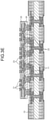
- FIG. 1 is a schematic sectional view of an example configuration of an interconnect board 1 according to an example.
- the upper surface in FIG. 1 will be referred to as a “top surface”, and the lower surface in FIG. 1 will be referred to as a “bottom surface”.
- the interconnect board 1 includes a lower substrate 10 and an upper substrate 20 .
- the lower substrate 10 and the upper substrate 20 are bonded to each other with an adhesive layer 30 .
- the lower substrate 10 is, for example, a multilayer build-up substrate.
- the lower substrate 10 has a plurality of electrodes 11 on its top surface, and has a plurality of electrodes 12 on its bottom surface.
- the electrodes 11 will be collectively referred to as an “electrode 11 ” as appropriate unless otherwise specified.
- the electrodes 12 will be collectively referred to as an “electrode 12 ” as appropriate unless otherwise specified.
- the inside of the lower substrate 10 has interconnect layers electrically interconnecting the electrode 11 and the electrode 12 .
- the top surface and the bottom surface of the lower substrate 10 have solder resist selectively applied in a manner of avoiding the electrode 11 and the electrode 12 .
- the lower substrate 10 is an example of a first substrate.
- the upper substrate 20 is an interposer substrate that routes connection, for example, between the lower substrate 10 and a semiconductor chip.
- the upper substrate 20 has a smaller outer shape than that of the lower substrate 10 , and is mounted on the lower substrate 10 .
- the upper substrate 20 has a plurality of electrodes 21 to be connected to chips on its top surface, and has a plurality of electrodes 22 on its bottom surface.
- the electrodes 21 to be connected to chips will be collectively referred to as a “chip electrode 21 ” as appropriate unless otherwise specified.
- the electrodes 22 will be collectively referred to as an “electrode 22 ” as appropriate unless otherwise specified.
- An interconnect layer is formed inside the upper substrate 20 to electrically interconnect the chip electrode 21 and the electrode 22 .
- the electrode 22 is connected to the electrode 11 on the top surface of the lower substrate 10 by a solder 23 , such as a solder ball and a solder bump.
- the upper substrate 20 is electrically connected with the lower substrate 10 .
- the upper substrate 20 is an example of a second substrate.
- the adhesive layer 30 examples include a nonconductive film made of a thermosetting resin.
- the adhesive layer 30 is used to reduce the stress between the lower substrate 10 and the upper substrate 20 , and to bond the lower substrate 10 and upper substrate 20 to each other.
- the outer edge portion of the adhesive layer 30 forms a fillet, which is a portion sticking out beyond the side surface of the upper substrate 20 and contacting the side surface of the upper substrate 20 .
- the outer edge portion of the adhesive layer 30 will be referred to as a “fillet” as appropriate.
- the fillet of the adhesive layer 30 has a raised portion 31 raised from the level of the top surface of the upper substrate 20 to a level higher than the top surface of the upper substrate 20 .
- the raised portion 31 is a frame-like portion arranged along the outer periphery of the upper substrate 20 .
- the raised portion 31 forms a bottomed space in combination with the top surface of the upper substrate 20 .
- the raised portion 31 is high enough to block an underfill resin, which fills the gap between the top surface of the upper substrate 20 and a semiconductor chip mounted thereon, from outflowing. In this structure, the raised portion 31 forms a bottomed space capable of storing the underfill resin, on the top surface of the upper substrate 20 .
- the upper substrate 20 having the adhesive layer 30 is mounted on the lower substrate 10 with the adhesive layer 30 held therebetween.
- the upper substrate 20 is then pressed against the lower substrate 10 with a bonding tool.
- the adhesive layer 30 held between the lower substrate 10 and the upper substrate 20 has an outer edge portion extended in a direction perpendicular (that is, horizontally) to the direction of thickness of the adhesive layer 30 .
- the extended outer edge portion sticks out beyond the side surface of the upper substrate 20 and forms a fillet.
- the fillet formed at the adhesive layer 30 is horizontally extended along the top surface of the lower substrate 10 , usable space on the top surface of the lower substrate 10 is narrowed due to the fillet. As a result, it becomes difficult to secure areas for mounting devices around the fillet.
- the interconnect board 1 of this example is configured such that the fillet, sticking out beyond the side surface of the upper substrate 20 , has the raised portion 31 raised to a level higher than the level of the top surface of the upper substrate 20 .
- the raised portion 31 allows the fillet to be increased in size in the direction of thickness of the adhesive layer 30 , and thus allows to be decreased in size in the horizontal direction.
- the fillet therefore occupies less space on the top surface of the lower substrate 10 . As a result, areas for mounting devices are sufficiently secured around the fillet.
- the interconnect board 1 of this example has the raised portion 31 formed as a frame-like portion arranged along the outer periphery of the upper substrate 20 .
- the raised portion 31 forms a bottomed space in combination with the top surface of the upper substrate 20 .
- This structure allows the underfill resin filling the bottomed space to be blocked by the raised portion 31 from outflowing toward the lower substrate 10 . Therefore, in the top surface of the lower substrate 10 , a situation that device mounting areas surrounding the upper substrate 20 and the adhesive layer 30 are invalidated by the underfill resin is avoided.
- FIG. 2 is a schematic sectional view of an example configuration of the semiconductor package 2 fabricated using the interconnect board 1 of the example.
- the semiconductor package 2 includes the lower substrate 10 , the upper substrate 20 , and the adhesive layer 30 for bonding the lower substrate 10 and the upper substrate 20 together.
- the semiconductor package 2 further includes semiconductor chips 40 , an underfill resin 50 , chip devices 61 , and reinforcing members 62 .
- the lower substrate 10 , the upper substrate 20 , and the adhesive layer 30 respectively correspond to the lower substrate 10 , the upper substrate 20 , and the adhesive layer 30 as illustrated in FIG. 1 .
- Examples of the semiconductor chip 40 include an integrated circuit such as large scale integration (LSI).
- the semiconductor chip 40 is mounted on the chip electrode 21 , for example, by the flip-chip technology, on the top surface of the upper substrate 20 .
- the semiconductor chip 40 is connected to the chip electrode 21 on the upper substrate 20 through solder bumps.
- the semiconductor chip 40 is an example of a semiconductor device.
- the underfill resin 50 is arranged in the bottomed space formed by the raised portion 31 of the fillet of the adhesive layer 30 and the top surface of the upper substrate 20 and bonds the upper substrate 20 and the semiconductor chip 40 together.
- Examples of the chip device 61 include a resistor and a capacitor, and the chip device is mounted on an area surrounding the upper substrate 20 and the adhesive layer 30 , in the top surface of the lower substrate 10 .
- the reinforcing member 62 is used to reinforce the semiconductor package 2 , and is mounted on an area surrounding the upper substrate 20 and the adhesive layer 30 , in the top surface of the lower substrate 10 .
- the reinforcing member 62 can keep the semiconductor package 2 from being warped.
- FIG. 3A to FIG. 3I are illustrative drawings of an example flow to fabricate the interconnect board 1 of the example.
- the upper substrate 20 is fabricated with the chip electrode 21 arranged on the top surface thereof and the electrode 22 on the bottom surface thereof.
- the upper substrate 20 is fabricated, for example, using the build-up technology.
- a solder 23 is deposited on the electrode 22 on the bottom surface of the upper substrate 20 .
- the adhesive layer 30 is formed on the bottom surface of the upper substrate 20 .
- the adhesive layer 30 is a non-conductive film made of a thermosetting resin
- the adhesive layer 30 is attached to the bottom surface of the upper substrate 20 .
- the upper substrate 20 is cut into separate pieces by a blade 70 .
- the upper substrate 20 with the adhesive layer 30 is fabricated.
- the upper substrate 20 with the adhesive layer 30 is arranged on the lower substrate 10 with the adhesive layer 30 held therebetween.
- the upper substrate 20 and the lower substrate 10 are positioned to each other such that the solder 23 deposited on the electrode 22 on the bottom surface of the upper substrate 20 faces the electrode 11 on the top surface of the lower substrate 10 .
- a bonding tool 80 is placed to contact the upper substrate 20 through a release sheet 81 .
- the bonding tool 80 is maintained at a temperature lower than the melting point of the solder 23 .
- the bonding tool 80 has a contact surface to contact the top surface of the upper substrate 20 , and the size of the contact surface is substantially as large as that of the top surface of the upper substrate 20 .
- a portion, of the release sheet 81 , not contacting the contact surface of the bonding tool 80 is folded obliquely upward from the plane where the top surface of the upper substrate 20 is located. The gap between the release sheet 81 and the top surface of the lower substrate 10 in the direction of thickness of the adhesive layer 30 is therefore increased at areas outside the side surface of the upper substrate 20 .
- the bonding tool 80 presses the upper substrate 20 against the lower substrate 10 .
- the bonding tool 80 continues pressing the upper substrate 20 against the lower substrate 10 until a fillet of the adhesive layer 30 is formed and raised from the level of the top surface of the upper substrate 20 to a level higher than the top surface of the upper substrate 20 to form the raised portion 31 .
- the raised portion 31 is formed with the fillet, as a portion of the adhesive layer 30 sticking out beyond the side surface of the upper substrate 20 , passing through the gap between the release sheet 81 and the top surface of the lower substrate 10 and raised in the direction of thickness of the adhesive layer 30 .
- the increase in size of the fillet in the direction of thickness of the adhesive layer 30 keeps the fillet from being horizontally extended.
- the fillet therefore occupies less space on the top surface of the lower substrate 10 .
- areas for mounting devices are sufficiently secured around the fillet.
- the bonding tool 80 further presses the upper substrate 20 until the raised portion 31 becomes high enough to block the underfill resin 50 (see FIG. 2 ), filling the gap between the top surface of the upper substrate 20 and the semiconductor chip 40 mounted thereon, from overflowing.
- the raised portion 31 creates a bottomed space capable of storing the underfill resin 50 , on the top surface of the upper substrate 20 .
- the bonding tool 80 is heated to cure the adhesive layer 30 and to solder the electrode 22 on the upper substrate 20 and the electrode 11 on the lower substrate 10 .
- the bonding tool 80 is heated to a temperature equal to or higher than the melting point of the solder 23 deposited on the electrode 22 on the bottom surface of the upper substrate 20 .
- the heated bonding tool allows the lower substrate 10 and the upper substrate 20 to be bonded together through the adhesive layer 30 , and melts the solder 23 to connect the electrode 22 on the upper substrate 20 and the electrode 11 on the lower substrate 10 .
- the bonding tool 80 and the release sheet 81 are separated from the upper substrate 20 , and the interconnect board 1 is fabricated.
- the process of FIG. 3H is conducted after the process of FIG. 3G ; however, these two processes may be conducted together.
- the process of pressing the upper substrate 20 against the lower substrate 10 and the process of curing the adhesive layer 30 and soldering the electrode 22 on the upper substrate 20 and the electrode 11 on the lower substrate 10 may be conducted at the same time.
- FIG. 4A to FIG. 4C are illustrative drawings of an example flow to fabricate the semiconductor package 2 of the example.
- the interconnect board 1 is fabricated in the processes of FIG. 3A to FIG. 3I .
- the semiconductor chip 40 is mounted on the chip electrode 21 on the upper substrate 20 using the flip-chip technology.
- the semiconductor chip 40 is connected to the chip electrode 21 on the upper substrate 20 through solder bumps.
- the gap between the top surface of the upper substrate 20 and the semiconductor chip 40 is filled with the underfill resin 50 .
- a bottomed space capable of storing the underfill resin 50 is formed on the top surface of the upper substrate 20 using the raised portion 31 of the adhesive layer 30 , and the bottomed space blocks the underfill resin 50 from overflowing to the lower substrate 10 . Therefore, in the top surface of the lower substrate 10 , a situation that device mounting areas surrounding the upper substrate 20 and the adhesive layer 30 are invalidated by the underfill resin 50 is avoided.
- components such as the chip device 61 and the reinforcing member 62 are mounted on the device mounting areas surrounding the upper substrate 20 and the adhesive layer 30 , in the top surface of the lower substrate 10 .
- the semiconductor package 2 is completed in this manner.
- the interconnect board 1 of the example includes the lower substrate 10 , the upper substrate 20 mounted on the lower substrate 10 , and the adhesive layer 30 that bonds the lower substrate 10 and the upper substrate 20 together and has a fillet contacting the side surface of the upper substrate 20 .
- the fillet of the adhesive layer 30 has the raised portion 31 raised from the level of the top surface of the upper substrate 20 to a level higher than the top surface of the upper substrate 20 .
- the fillet is increased in size in the direction of thickness of the adhesive layer 30 , and is thus decreased in size in the horizontal direction.
- the fillet therefore occupies less space on the top surface of the lower substrate 10 . Areas for mounting devices, such as the chip device 61 and the reinforcing member 62 , are therefore sufficiently secured around the fillet.
- the interconnect board 1 of the example has the raised portion 31 formed as a frame-like portion arranged along the outer periphery of the upper substrate 20 .
- the raised portion 31 forms a bottomed space in combination with the top surface of the upper substrate 20 .
- the raised portion 31 blocks the underfill resin 50 filling the bottomed space from overflowing to the lower substrate 10 . Therefore, in the top surface of the lower substrate 10 , a situation that device mounting areas surrounding the upper substrate 20 and the adhesive layer 30 are invalidated by the underfill resin 50 is avoided.
- areas for mounting devices are sufficiently secured around the fillet.
- a method of fabricating an interconnect board comprising:
Landscapes
- Engineering & Computer Science (AREA)
- Microelectronics & Electronic Packaging (AREA)
- Power Engineering (AREA)
- Computer Hardware Design (AREA)
- Physics & Mathematics (AREA)
- Condensed Matter Physics & Semiconductors (AREA)
- General Physics & Mathematics (AREA)
- Wire Bonding (AREA)
- Non-Metallic Protective Coatings For Printed Circuits (AREA)
- Combinations Of Printed Boards (AREA)
- Manufacturing & Machinery (AREA)
Abstract
Description
Claims (14)
Applications Claiming Priority (3)
| Application Number | Priority Date | Filing Date | Title |
|---|---|---|---|
| JPJP2018-243631 | 2018-12-26 | ||
| JP2018-243631 | 2018-12-26 | ||
| JP2018243631A JP7236269B2 (en) | 2018-12-26 | 2018-12-26 | Wiring board, semiconductor device, and wiring board manufacturing method |
Publications (2)
| Publication Number | Publication Date |
|---|---|
| US20200211946A1 US20200211946A1 (en) | 2020-07-02 |
| US11233001B2 true US11233001B2 (en) | 2022-01-25 |
Family
ID=71124172
Family Applications (1)
| Application Number | Title | Priority Date | Filing Date |
|---|---|---|---|
| US16/712,347 Active US11233001B2 (en) | 2018-12-26 | 2019-12-12 | Adhesive layer bonding a plurality of substrates having a fillet raised portion |
Country Status (2)
| Country | Link |
|---|---|
| US (1) | US11233001B2 (en) |
| JP (1) | JP7236269B2 (en) |
Cited By (1)
| Publication number | Priority date | Publication date | Assignee | Title |
|---|---|---|---|---|
| US20240412982A1 (en) * | 2023-06-08 | 2024-12-12 | Taiwan Semiconductor Manufacturing Company, Ltd. | Semiconductor structure and manufacturing method thereof |
Families Citing this family (8)
| Publication number | Priority date | Publication date | Assignee | Title |
|---|---|---|---|---|
| US11728278B2 (en) * | 2019-03-25 | 2023-08-15 | Taiwan Semiconductor Manufacturing Company, Ltd. | Board substrates, three-dimensional integrated circuit structures and methods of forming the same |
| KR102841472B1 (en) * | 2020-07-10 | 2025-08-05 | 삼성전자주식회사 | Semiconductor package |
| JPWO2022202553A1 (en) | 2021-03-22 | 2022-09-29 | ||
| EP4319509A4 (en) | 2021-03-22 | 2024-10-30 | Panasonic Intellectual Property Management Co., Ltd. | WIRING TRANSFER PLATE, WIRING TRANSFER PLATE, INTERMEDIATE MATERIAL FOR A WIRING BODY AND METHOD FOR PRODUCING A WIRING BODY |
| WO2022202548A1 (en) | 2021-03-22 | 2022-09-29 | パナソニックIpマネジメント株式会社 | Wiring body, mounting substrate, wiring transfer plate with wiring, intermediate material for wiring body, manufacturing method for wiring body, and manufacturing method for mounting substrate |
| WO2022202547A1 (en) | 2021-03-22 | 2022-09-29 | パナソニックIpマネジメント株式会社 | Wiring body, mounting substrate, method for manufacturing wiring body, and method for manufacturing mounting substrate |
| US12388001B2 (en) | 2021-08-27 | 2025-08-12 | Advanced Semiconductor Engineering, Inc. | Electronic package |
| CN114068476B (en) * | 2021-10-13 | 2025-12-23 | 日月光半导体制造股份有限公司 | Semiconductor packaging structure and its formation method |
Citations (15)
| Publication number | Priority date | Publication date | Assignee | Title |
|---|---|---|---|---|
| JP2004079658A (en) | 2002-08-13 | 2004-03-11 | Fujitsu Ltd | Semiconductor device and manufacturing method thereof |
| US20070246815A1 (en) * | 2006-04-21 | 2007-10-25 | Yung-Li Lu | Stackable semiconductor package |
| US20070278640A1 (en) * | 2006-05-30 | 2007-12-06 | Gwo-Liang Weng | Stackable semiconductor package |
| US20070278696A1 (en) * | 2006-05-30 | 2007-12-06 | Yung-Li Lu | Stackable semiconductor package |
| US20080157325A1 (en) * | 2006-12-31 | 2008-07-03 | Seng Guan Chow | Integrated circuit package with molded cavity |
| US20090091015A1 (en) * | 2007-10-05 | 2009-04-09 | Advanced Semiconductor Engineering, Inc. | Stacked-type chip package structure and method of fabricating the same |
| US20090284947A1 (en) * | 2008-05-19 | 2009-11-19 | Stanley Craig Beddingfield | Integrated circuit package having integrated faraday shield |
| US20100244223A1 (en) * | 2009-03-25 | 2010-09-30 | Cho Namju | Integrated circuit packaging system with an integral-interposer-structure and method of manufacture thereof |
| US20110241168A1 (en) * | 2010-03-31 | 2011-10-06 | Yong-Hoon Kim | Package on package structure |
| US20120211885A1 (en) * | 2011-02-17 | 2012-08-23 | Choi Yunseok | Semiconductor package having through silicon via (tsv) interposer and method of manufacturing the semiconductor package |
| US20130075915A1 (en) * | 2011-09-23 | 2013-03-28 | DaeSup Kim | Integrated circuit packaging system with chip stacking and method of manufacture thereof |
| US8791562B2 (en) * | 2010-07-21 | 2014-07-29 | Samsung Electronics Co., Ltd. | Stack package and semiconductor package including the same |
| US20140299980A1 (en) * | 2013-04-05 | 2014-10-09 | Samsung Electronics Co., Ltd. | Semiconductor packages including a heat spreader and methods of forming the same |
| US20150003029A1 (en) * | 2013-06-28 | 2015-01-01 | Canon Kabushiki Kaisha | Stacked semiconductor device, printed circuit board, and method for manufacturing stacked semiconductor device |
| US20160141271A1 (en) * | 2014-11-14 | 2016-05-19 | Kang Joon LEE | Semiconductor packages and methods of fabricating the same |
Family Cites Families (3)
| Publication number | Priority date | Publication date | Assignee | Title |
|---|---|---|---|---|
| KR101719636B1 (en) * | 2011-01-28 | 2017-04-05 | 삼성전자 주식회사 | Semiconductor device and fabricating method thereof |
| JP2015133367A (en) * | 2014-01-10 | 2015-07-23 | 富士通株式会社 | Method of manufacturing electronic apparatus and electronic apparatus |
| JP6478853B2 (en) * | 2015-07-14 | 2019-03-06 | 新光電気工業株式会社 | Electronic component device and manufacturing method thereof |
-
2018
- 2018-12-26 JP JP2018243631A patent/JP7236269B2/en active Active
-
2019
- 2019-12-12 US US16/712,347 patent/US11233001B2/en active Active
Patent Citations (15)
| Publication number | Priority date | Publication date | Assignee | Title |
|---|---|---|---|---|
| JP2004079658A (en) | 2002-08-13 | 2004-03-11 | Fujitsu Ltd | Semiconductor device and manufacturing method thereof |
| US20070246815A1 (en) * | 2006-04-21 | 2007-10-25 | Yung-Li Lu | Stackable semiconductor package |
| US20070278640A1 (en) * | 2006-05-30 | 2007-12-06 | Gwo-Liang Weng | Stackable semiconductor package |
| US20070278696A1 (en) * | 2006-05-30 | 2007-12-06 | Yung-Li Lu | Stackable semiconductor package |
| US20080157325A1 (en) * | 2006-12-31 | 2008-07-03 | Seng Guan Chow | Integrated circuit package with molded cavity |
| US20090091015A1 (en) * | 2007-10-05 | 2009-04-09 | Advanced Semiconductor Engineering, Inc. | Stacked-type chip package structure and method of fabricating the same |
| US20090284947A1 (en) * | 2008-05-19 | 2009-11-19 | Stanley Craig Beddingfield | Integrated circuit package having integrated faraday shield |
| US20100244223A1 (en) * | 2009-03-25 | 2010-09-30 | Cho Namju | Integrated circuit packaging system with an integral-interposer-structure and method of manufacture thereof |
| US20110241168A1 (en) * | 2010-03-31 | 2011-10-06 | Yong-Hoon Kim | Package on package structure |
| US8791562B2 (en) * | 2010-07-21 | 2014-07-29 | Samsung Electronics Co., Ltd. | Stack package and semiconductor package including the same |
| US20120211885A1 (en) * | 2011-02-17 | 2012-08-23 | Choi Yunseok | Semiconductor package having through silicon via (tsv) interposer and method of manufacturing the semiconductor package |
| US20130075915A1 (en) * | 2011-09-23 | 2013-03-28 | DaeSup Kim | Integrated circuit packaging system with chip stacking and method of manufacture thereof |
| US20140299980A1 (en) * | 2013-04-05 | 2014-10-09 | Samsung Electronics Co., Ltd. | Semiconductor packages including a heat spreader and methods of forming the same |
| US20150003029A1 (en) * | 2013-06-28 | 2015-01-01 | Canon Kabushiki Kaisha | Stacked semiconductor device, printed circuit board, and method for manufacturing stacked semiconductor device |
| US20160141271A1 (en) * | 2014-11-14 | 2016-05-19 | Kang Joon LEE | Semiconductor packages and methods of fabricating the same |
Cited By (1)
| Publication number | Priority date | Publication date | Assignee | Title |
|---|---|---|---|---|
| US20240412982A1 (en) * | 2023-06-08 | 2024-12-12 | Taiwan Semiconductor Manufacturing Company, Ltd. | Semiconductor structure and manufacturing method thereof |
Also Published As
| Publication number | Publication date |
|---|---|
| US20200211946A1 (en) | 2020-07-02 |
| JP7236269B2 (en) | 2023-03-09 |
| JP2020107681A (en) | 2020-07-09 |
Similar Documents
| Publication | Publication Date | Title |
|---|---|---|
| US11233001B2 (en) | Adhesive layer bonding a plurality of substrates having a fillet raised portion | |
| US9799611B2 (en) | Semiconductor device including semiconductor chips mounted over both surfaces of substrate | |
| US7790515B2 (en) | Semiconductor device with no base member and method of manufacturing the same | |
| JP5066529B2 (en) | Semiconductor element mounting structure and semiconductor element mounting method | |
| US20140295620A1 (en) | Method of manufacturing semiconductor device having plural semiconductor chips stacked one another | |
| US20110057327A1 (en) | Semiconductor device and method of manufacturing the same | |
| US9953958B2 (en) | Electronic component device | |
| JP6478853B2 (en) | Electronic component device and manufacturing method thereof | |
| KR20160006702A (en) | Semiconductor device and semiconductor device manufacturing method | |
| KR102066015B1 (en) | Semiconductor package and method of manufacturing the same | |
| US9449949B2 (en) | Method for manufacturing semiconductor device and semiconductor device | |
| US7755203B2 (en) | Circuit substrate and semiconductor device | |
| US10290570B2 (en) | Wiring substrate | |
| US7663254B2 (en) | Semiconductor apparatus and method of manufacturing the same | |
| KR20200108889A (en) | Semiconductor device and method of manufacturing semiconductor device | |
| TWI585919B (en) | Chip package substrate, chip package structure and manufacturing method thereof | |
| JP2013239660A (en) | Semiconductor device and method of manufacturing the same | |
| US7768140B2 (en) | Semiconductor device | |
| US20180301406A1 (en) | Semiconductor package and method for manufacturing the same | |
| JP2016082156A (en) | Electronic module and manufacturing method for the same | |
| US20160118322A1 (en) | Laminated substrate and method for manufacturing laminated substrate | |
| KR20070051165A (en) | Semiconductor package having pre-solder bumps, laminated package using same, and manufacturing method thereof | |
| KR20030085449A (en) | An improved flip chip package | |
| US20230411264A1 (en) | Laminated wiring board | |
| US10115694B2 (en) | Electronic device, electronic device fabrication method, and electronic apparatus |
Legal Events
| Date | Code | Title | Description |
|---|---|---|---|
| AS | Assignment |
Owner name: SHINKO ELECTRIC INDUSTRIES CO., LTD., JAPAN Free format text: ASSIGNMENT OF ASSIGNORS INTEREST;ASSIGNORS:MIKI, SHOTA;KOBAYASHI, NAOKI;REEL/FRAME:051268/0908 Effective date: 20191120 |
|
| FEPP | Fee payment procedure |
Free format text: ENTITY STATUS SET TO UNDISCOUNTED (ORIGINAL EVENT CODE: BIG.); ENTITY STATUS OF PATENT OWNER: LARGE ENTITY |
|
| STPP | Information on status: patent application and granting procedure in general |
Free format text: DOCKETED NEW CASE - READY FOR EXAMINATION |
|
| STPP | Information on status: patent application and granting procedure in general |
Free format text: NON FINAL ACTION MAILED |
|
| STPP | Information on status: patent application and granting procedure in general |
Free format text: RESPONSE TO NON-FINAL OFFICE ACTION ENTERED AND FORWARDED TO EXAMINER |
|
| STPP | Information on status: patent application and granting procedure in general |
Free format text: FINAL REJECTION MAILED |
|
| STPP | Information on status: patent application and granting procedure in general |
Free format text: NON FINAL ACTION MAILED |
|
| STPP | Information on status: patent application and granting procedure in general |
Free format text: RESPONSE TO NON-FINAL OFFICE ACTION ENTERED AND FORWARDED TO EXAMINER |
|
| STPP | Information on status: patent application and granting procedure in general |
Free format text: NOTICE OF ALLOWANCE MAILED -- APPLICATION RECEIVED IN OFFICE OF PUBLICATIONS |
|
| STPP | Information on status: patent application and granting procedure in general |
Free format text: PUBLICATIONS -- ISSUE FEE PAYMENT VERIFIED |
|
| STCF | Information on status: patent grant |
Free format text: PATENTED CASE |
|
| MAFP | Maintenance fee payment |
Free format text: PAYMENT OF MAINTENANCE FEE, 4TH YEAR, LARGE ENTITY (ORIGINAL EVENT CODE: M1551); ENTITY STATUS OF PATENT OWNER: LARGE ENTITY Year of fee payment: 4 |