US11229115B2 - Wiring board and electronic device - Google Patents
Wiring board and electronic device Download PDFInfo
- Publication number
- US11229115B2 US11229115B2 US16/758,463 US201716758463A US11229115B2 US 11229115 B2 US11229115 B2 US 11229115B2 US 201716758463 A US201716758463 A US 201716758463A US 11229115 B2 US11229115 B2 US 11229115B2
- Authority
- US
- United States
- Prior art keywords
- holes
- differential signal
- pads
- hole
- arrangement direction
- Prior art date
- Legal status (The legal status is an assumption and is not a legal conclusion. Google has not performed a legal analysis and makes no representation as to the accuracy of the status listed.)
- Active
Links
Images


Classifications
-
- H—ELECTRICITY
- H05—ELECTRIC TECHNIQUES NOT OTHERWISE PROVIDED FOR
- H05K—PRINTED CIRCUITS; CASINGS OR CONSTRUCTIONAL DETAILS OF ELECTRIC APPARATUS; MANUFACTURE OF ASSEMBLAGES OF ELECTRICAL COMPONENTS
- H05K1/00—Printed circuits
- H05K1/02—Details
- H05K1/0213—Electrical arrangements not otherwise provided for
- H05K1/0216—Reduction of cross-talk, noise or electromagnetic interference
- H05K1/0228—Compensation of cross-talk by a mutually correlated lay-out of printed circuit traces, e.g. for compensation of cross-talk in mounted connectors
-
- H—ELECTRICITY
- H05—ELECTRIC TECHNIQUES NOT OTHERWISE PROVIDED FOR
- H05K—PRINTED CIRCUITS; CASINGS OR CONSTRUCTIONAL DETAILS OF ELECTRIC APPARATUS; MANUFACTURE OF ASSEMBLAGES OF ELECTRICAL COMPONENTS
- H05K1/00—Printed circuits
- H05K1/02—Details
- H05K1/0213—Electrical arrangements not otherwise provided for
- H05K1/0237—High frequency adaptations
- H05K1/0245—Lay-out of balanced signal pairs, e.g. differential lines or twisted lines
-
- H—ELECTRICITY
- H05—ELECTRIC TECHNIQUES NOT OTHERWISE PROVIDED FOR
- H05K—PRINTED CIRCUITS; CASINGS OR CONSTRUCTIONAL DETAILS OF ELECTRIC APPARATUS; MANUFACTURE OF ASSEMBLAGES OF ELECTRICAL COMPONENTS
- H05K1/00—Printed circuits
- H05K1/02—Details
- H05K1/11—Printed elements for providing electric connections to or between printed circuits
- H05K1/111—Pads for surface mounting, e.g. lay-out
- H05K1/112—Pads for surface mounting, e.g. lay-out directly combined with via connections
- H05K1/113—Via provided in pad; Pad over filled via
-
- H—ELECTRICITY
- H05—ELECTRIC TECHNIQUES NOT OTHERWISE PROVIDED FOR
- H05K—PRINTED CIRCUITS; CASINGS OR CONSTRUCTIONAL DETAILS OF ELECTRIC APPARATUS; MANUFACTURE OF ASSEMBLAGES OF ELECTRICAL COMPONENTS
- H05K1/00—Printed circuits
- H05K1/02—Details
- H05K1/0213—Electrical arrangements not otherwise provided for
- H05K1/0216—Reduction of cross-talk, noise or electromagnetic interference
- H05K1/0218—Reduction of cross-talk, noise or electromagnetic interference by printed shielding conductors, ground planes or power plane
- H05K1/0219—Printed shielding conductors for shielding around or between signal conductors, e.g. coplanar or coaxial printed shielding conductors
-
- H—ELECTRICITY
- H05—ELECTRIC TECHNIQUES NOT OTHERWISE PROVIDED FOR
- H05K—PRINTED CIRCUITS; CASINGS OR CONSTRUCTIONAL DETAILS OF ELECTRIC APPARATUS; MANUFACTURE OF ASSEMBLAGES OF ELECTRICAL COMPONENTS
- H05K1/00—Printed circuits
- H05K1/02—Details
- H05K1/11—Printed elements for providing electric connections to or between printed circuits
- H05K1/111—Pads for surface mounting, e.g. lay-out
- H05K1/112—Pads for surface mounting, e.g. lay-out directly combined with via connections
- H05K1/114—Pad being close to via, but not surrounding the via
-
- H—ELECTRICITY
- H05—ELECTRIC TECHNIQUES NOT OTHERWISE PROVIDED FOR
- H05K—PRINTED CIRCUITS; CASINGS OR CONSTRUCTIONAL DETAILS OF ELECTRIC APPARATUS; MANUFACTURE OF ASSEMBLAGES OF ELECTRICAL COMPONENTS
- H05K2201/00—Indexing scheme relating to printed circuits covered by H05K1/00
- H05K2201/09—Shape and layout
- H05K2201/09209—Shape and layout details of conductors
- H05K2201/09372—Pads and lands
- H05K2201/09409—Multiple rows of pads, lands, terminals or dummy patterns; Multiple rows of mounted components
-
- H—ELECTRICITY
- H05—ELECTRIC TECHNIQUES NOT OTHERWISE PROVIDED FOR
- H05K—PRINTED CIRCUITS; CASINGS OR CONSTRUCTIONAL DETAILS OF ELECTRIC APPARATUS; MANUFACTURE OF ASSEMBLAGES OF ELECTRICAL COMPONENTS
- H05K2201/00—Indexing scheme relating to printed circuits covered by H05K1/00
- H05K2201/09—Shape and layout
- H05K2201/09209—Shape and layout details of conductors
- H05K2201/095—Conductive through-holes or vias
- H05K2201/09609—Via grid, i.e. two-dimensional array of vias or holes in a single plane
-
- H—ELECTRICITY
- H05—ELECTRIC TECHNIQUES NOT OTHERWISE PROVIDED FOR
- H05K—PRINTED CIRCUITS; CASINGS OR CONSTRUCTIONAL DETAILS OF ELECTRIC APPARATUS; MANUFACTURE OF ASSEMBLAGES OF ELECTRICAL COMPONENTS
- H05K2201/00—Indexing scheme relating to printed circuits covered by H05K1/00
- H05K2201/10—Details of components or other objects attached to or integrated in a printed circuit board
- H05K2201/10007—Types of components
- H05K2201/10189—Non-printed connector
Definitions
- the present invention relates to a wiring board and an electronic device.
- PTL 1 discloses that “when a high-speed differential signal is transmitted to a differential wiring through a via hole with an open stub, a waveform distortion occurs due to an impedance mismatch at the open stub of the via and causes a jitter, which is a problem of speed-up”, and “for the differential wiring passing through the via hole with the open stub, a degree of coupling is reduced while a differential characteristic impedance is kept constant. Therefore, an influence of rear crosstalk noise due to the coupling can be reduced to a small value, so that the jitter can be prevented”.
- PTL 2 discloses that “Provided is a multilayer wiring board or the like which can reduce crosstalk between differential wirings disposed in each signal layer between ground layers”, and “There is a multilayer wiring board 1 in which a plurality of signal layers 3 and ground layers 2 are laminated.
- the ground layer includes a first clearance 141 through which a first differential signal via 12 A is inserted without coming into contact with a wiring of the ground layer, and a second clearance 142 through which a second differential signal via 12 B is inserted without coming into contact with the wiring of the ground layer.
- a distance Rx between an outer edge portion of the first clearance on the side of the second differential signal via and the first differential signal via is set to be shorter than a distance Rmax between an outer edge portion of the first clearance on the side opposite to the second differential signal via and the first differential signal.
- a distance between an outer edge portion of the second clearance on the side of the first differential signal via and the second differential signal via is set to be shorter than the distance between the outer edge portion of the second clearance on the side opposite to the first differential signal via and the second differential signal via”.
- an electronic device configured by using a large number of electronic components such as an integrated circuit, a large number of signal lines and power supply lines, ground lines, and the like for electrically connecting the electronic components are required to be efficiently wired at high density, and a multilayer wiring board is used as a wiring board.
- a plurality of pads aligned at a predetermined pitch on which a multi-pin electronic component such as an integrated circuit or a surface mount connector is mounted and each pin is soldered.
- Each of a plurality of pads is electrically connected to a through hole that electrically connects layers of the wiring board via a wiring pattern.
- the electronic component cannot be mounted in a region where the through hole is disposed, it is necessary to make the region as small as possible in order to mount the electronic component at high density on the wiring board.
- the electronic component having a narrow pitch of pins is frequently used in wiring boards in order to achieve miniaturization or ensure compatibility with existing interfaces, and a pitch of pads on the wiring board is also narrowed.
- the through hole needs to be formed by drilling, it is difficult to reduce the diameter and ensure the accuracy of a hole position, and there is a limit to adjust an interval of the through holes according to the pitch of the pads.
- an air hole for allowing cooling air to pass through may be provided in the wiring board accommodated in a housing of the electronic device, in this case, it is necessary to prevent an area of the air hole from being pressed by the through hole or the wiring pattern provided in the wiring board.
- a power supply via hole and a signal via hole are linearly arranged in a drawing direction, and a region of the via hole inevitably becomes large. Further, the crosstalk may occur because the signal via holes are adjacent to each other in a direction perpendicular to the drawing direction.
- the vias are linearly arranged in a direction in which the differential wiring extends, and a region of the via inevitably becomes large. Also, there is a portion where the differential signal vias are adjacent to each other between the pair of adjacent differential signal vias, which may cause crosstalk.
- the invention is made in view of such a background, and an object of the invention is to provide a wiring board capable of efficiently performing wiring at high density while preventing the crosstalk of the differential signals and an electronic device using the same.
- a multilayer wiring board including a plurality of pads linearly arranged at a predetermined pitch; a plurality of through holes arranged in parallel along an arrangement direction of the pads; and a wiring pattern connecting the pad to the through hole. Between the through holes connected to the pads which are connected to the ground via the wiring patterns, two through holes through which each of a pair of differential signals constituting a differential signal pair passes are provided such that a direction of a straight line connecting the two through holes is inclined to the arrangement direction of the pads.
- the wiring board capable of efficiently performing wiring at high density while preventing the crosstalk of the differential signals and the electronic device using the same.
- FIG. 1 is a diagram illustrating a schematic configuration of a wiring board.
- FIG. 2 is a diagram illustrating a configuration of a first comparative example.
- FIG. 3 is a diagram illustrating a configuration of a second comparative example.
- FIG. 4 is a diagram illustrating a configuration of a first embodiment.
- FIG. 5 is a partial cross-sectional view of the wiring board having the configuration of FIG. 4 taken along a line A-A′ of FIG. 4 .
- FIG. 6 is a graph illustrating pass characteristics of a differential signal of the wiring board of the second comparative example.
- FIG. 7 is a graph illustrating pass characteristics of a differential signal of the wiring board of the first embodiment.
- FIG. 8 is a graph illustrating crosstalk of the wiring board of the second comparative example.
- FIG. 9 is a graph illustrating crosstalk of the wiring board of the first embodiment.
- FIG. 10 is a diagram illustrating a configuration of a second embodiment.
- FIG. 11 is a diagram illustrating a configuration of a third embodiment.
- FIG. 12 is a diagram illustrating a configuration of a fourth embodiment.
- FIG. 1 is a diagram illustrating a schematic configuration of a printed wiring board (hereinafter, referred to as a wiring board 1 ) according to an embodiment, and a perspective view of a part of the wiring board 1 as viewed from a surface side (+z side shown in FIG. 1 ).
- the wiring board 1 is, for example, a component of an electronic device such as a blade server or a storage device.
- the wiring board 1 is mounted as, for example, a midplane, a backplane, or the like in a housing of the electronic device.
- the wiring board 1 is a multilayer (laminated) wiring board having a multilayer (laminated) structure in which a plurality of layers such as a signal layer, a wiring layer, a power supply layer, and a ground layer are laminated. Further, note that the diagram only schematically illustrates a configuration of a surface of the wiring board 1 , and the detailed configuration of the surface of the wiring board 1 will be clarified by the following description and other drawings.
- a surface mounted multi-pin electronic component such as an integrated circuit or a surface mount connector is mounted on the surface of the wiring board 1 .
- a plurality of board-to-board connectors hereinafter, referred to as connectors 2
- connectors 2 board-to-board connectors
- the connector 2 includes a socket 21 extending parallel to a lateral direction (x-axis direction) of the wiring board 1 , and a pedestal portion 22 serving as a base of the socket 21 .
- the pins 23 of the connector 2 are provided so as to be aligned along a longitudinal direction of the connector 2 .
- Each pin 23 of the connector 2 extends downward ( ⁇ z direction) from a lower surface of the pedestal portion 22 and an end portion thereof is bent in a direction (-y direction) away from the pedestal portion 22 .
- aboard (blade, card, or the like) on which electronic components such as an arithmetic unit and an I/O unit are mounted is mounted on the socket 21 .
- pads 3 On the surface of the wiring board 1 , there are provided a plurality of conductor pads (hereinafter, referred to as pads 3 ) linearly aligned in the lateral direction (x-axis direction) of the wiring board 1 with a pitch the same as the pitch of the pins 23 of the connector 2 .
- the pads 3 are formed in a rectangular shape with the same shape and the same size having a longitudinal side parallel to a y-axis and a lateral side parallel to an x-axis.
- Each pin 23 of the connector 2 is soldered and electrically connected to the corresponding pad 3 .
- a rectangular air hole 12 for passing cooling air flowing inside the housing in which the wiring board 1 is accommodated is provided in a region sandwiched between two adjacent connectors 2 on the surface of the wiring board 1 .
- the longitudinal side of the air hole 12 is parallel to the lateral direction (x-axis direction) of the wiring board 1
- the lateral side of the air hole 12 is parallel to the longitudinal direction (y-axis direction) of the wiring board 1 .
- the length of the longitudinal side of the air hole 12 is the same as the length of the connector 2 in the longitudinal direction.
- a substantially rectangular through hole forming region 13 is provided adjacent to the plurality of pads 3 arranged in alignment.
- a plurality of through holes 5 electrically connected to the corresponding pads 3 via wiring patterns 6 to be described later are formed in the through hole forming region 13 .
- the through hole 5 is electrically connected to a predetermined layer of the wiring board 1 .
- a substantially rectangular region (hereinafter, referred to as a blank region 14 ) in which no through hole 5 is formed is provided between the through hole forming region 13 and the air hole 12 .
- the blank region 14 is provided for, for example, ensuring strength of the wiring board 1 .
- the connector 2 has a similar structure on the +y side as the structure on the ⁇ y side (the pin 23 , the pad 3 , the through hole forming region 13 , the blank region 14 , or the like).
- FIG. 2 is a configuration example (hereinafter, referred to as a first comparative example) of the periphery of the pads 3 and the through hole forming region 13 shown in FIG. 1 , and a plan view of a part of the periphery of the pads 3 and the through hole forming region 13 shown in FIG. 1 as viewed from the +z direction in FIG. 1 .
- the pads 3 b , 3 c , 3 e , and 3 f shown in white are all pads through which a differential signal passes (hereinafter, also referred to as differential signal pads 3 ).
- the differential signal pad 3 b and the differential signal pad 3 c , the differential signal pad 3 e and the differential signal pad 3 f respectively constitute a differential signal pair (positive and negative signals constituting a pair of differential signals, hereinafter, referred to as a differential signal pair) in differential transmission.
- PCI Express PCI Express
- USB universal serial bus
- SATA serial ATA
- HDMI High-Definition Multimedia Interface
- HDMI High-Definition Multimedia Interface
- HDMI High-Definition Multimedia Interface
- LVDS low voltage differential signaling
- the pads 3 a , 3 d , and 3 g which are shaded, are all ground pads (hereinafter, also referred to as ground pads 3 ).
- through holes 5 b , 5 c , 5 e , and 5 f shown in white are all through holes (hereinafter, also referred to as differential signal through holes 5 ) through which the differential signals pass.
- a signal passing through the differential signal through hole 5 b and a signal passing through the differential signal through hole 5 c , a signal passing through the differential signal through hole 5 e and a signal passing through the differential signal through hole 5 f respectively constitute the differential signal pair.
- clearances 7 a and 7 b for ensuring insulation are provided around two differential signal through holes 5 in each differential signal pair.
- the through holes 5 a , 5 d , and 5 g which are shaded, are all ground through holes (hereinafter, also referred to as ground through holes 5 ).
- the plurality of pads 3 are electrically connected to the corresponding through holes 5 through the wiring patterns 6 made of a conductor such as a copper foil. That is, the pad 3 a is electrically connected to the through hole 5 a via a wiring pattern 6 a , the pad 3 b is electrically connected to the through hole 5 b via a wiring pattern 6 b , the pad 3 c is electrically connected to the through hole 5 c via a wiring pattern 6 c , the pad 3 d is electrically connected to the through hole 5 d via a wiring pattern 6 d , the pad 3 e is electrically connected to the through hole 5 e via a wiring pattern 6 e , the pad 3 f is electrically connected to the through hole 5 f via a wiring pattern 6 f , and the pad 3 g is electrically connected to the through hole 5 g via a wiring pattern 6 g.
- the pad 3 a is electrically connected to the through hole 5 a via a wiring pattern 6 a
- the pad 3 b is
- the through holes 5 a to 5 g can be linearly arranged in the alignment direction of the pads 3 (x-axis direction), and the through hole forming region 13 can be made small. Therefore, it is possible to increase the area of the air hole 12 in the wiring board 1 . As shown in the figure, since the ground through hole 5 is interposed between the differential signal through holes 5 of adjacent differential signal pairs, a crosstalk between the adjacent differential signal pairs can be prevented.
- the through hole 5 needs to be formed by drilling, it is difficult to reduce the diameter and ensure the accuracy of the hole position, and it is difficult to make a pitch of the through holes 5 narrower than a predetermined lower limit value. Therefore, when a pitch of the pins 23 of the connector 2 is narrow and a pitch of the pads 3 is narrow, the through holes 5 a to 5 g cannot be linearly arranged in parallel (in the x-axis direction) in the alignment direction of the pads 3 as in the first comparative example.
- FIG. 3 is a configuration example of the periphery of the pads 3 and the through hole forming region 13 so as to be able to deal with a case where the pitch of the pads 3 is narrow (hereinafter, referred to as a second comparative example).
- the through holes 5 b , 5 c , 5 e , and 5 f for differential signals are provided at positions on an air hole 12 side away from the pads 3 than the through holes 5 a , 5 d , and 5 g for a ground line.
- the pitch of the pads 3 is narrow.
- the through hole forming region 13 expands, and a region for forming the air hole 12 is compressed.
- crosstalk occurs between the adjacent differential signal pairs without the ground through hole interposed between the through holes 5 of two adjacent differential signal pairs.
- FIG. 4 is a configuration example (hereinafter, referred to as a first embodiment) of the periphery of the pads 3 and the through hole forming region 13 for solving the above problem of the second comparative example.
- an arrangement direction of the differential signal through holes 5 of the differential signal pair (a direction of a straight line connecting centers of the through holes 5 which form the differential signal pair) is inclined by a predetermined angle (for example, 10 to 80 degrees) to an arrangement direction (x-axis direction) of the pads 3 .
- the ground through holes 5 are provided for each of the two differential signal through holes 5 of the differential signal pair, and each of the differential signal through holes 5 is located between the ground through holes 5 adjacent to each other in the arrangement direction (x-axis direction) of the pads 3 .
- the differential signal through hole 5 b is located between the ground through hole 5 a and the ground through hole 5 d
- the differential signal through hole 5 c is located between the ground through hole 5 a ′ and the ground through hole 5 d ′.
- the predetermined angle to, for example, 60 degrees
- all of the differential signal through holes 5 and the ground through holes 5 can be arranged at equal intervals, and the through holes 5 can be arranged at high density in the wiring board 1 .
- the differential signal through hole 5 is provided such that a center line Ct of the two differential signal through holes 5 constituting the differential signal pair is on the +x side (a differential signal pad 3 side connected to the differential signal through hole 5 located closer to the pad 3 among the two differential signal through holes 5 which constitute the differential signal pair) with respect to a center line Cp between two adjacent differential signal pads 3 . Therefore, the lengths of the two wiring patterns 6 connected to the respective differential signal through holes 5 can be equal to each other. Therefore, the in-phase noise superimposed on the wiring of the differential signal is cancelled, and the transmission quality can be ensured.
- the differential signal through hole 5 is interposed between the ground through holes 5 , the region for forming the air hole 12 is not compressed by the through hole forming region 13 . Further, since the ground through hole 5 is interposed between the through holes 5 of the adjacent differential signal pairs, a reduction effect of the crosstalk between two adjacent differential signal pairs can be expected.
- FIG. 5 is a view illustrating an internal structure of the wiring board 1 of FIG. 4 , and is a partial cross-sectional view of the wiring board 1 of FIG. 4 taken along a line A-A′.
- the differential signal pad 3 b is electrically connected to the differential signal wiring 7 of an inner layer via the wiring pattern 6 b and the differential signal through hole 5 b .
- the other pads 3 are electrically connected to the predetermined layer via the corresponding wiring patterns 6 and the through holes 5 , respectively.
- FIG. 6 is a graph illustrating pass characteristics of the differential signal of the wiring board 1 of the second comparative example
- FIG. 7 is a graph illustrating pass characteristics of the differential signal of the wiring board 1 of the first embodiment.
- the horizontal axis represents frequency (GHz)
- the vertical axis represents signal strength (dB).
- FIG. 8 is a graph illustrating a frequency characteristic of crosstalk of the wiring board 1 of the second comparative example
- FIG. 9 is a graph illustrating a frequency characteristic of crosstalk of the wiring board 1 of the first embodiment.
- the horizontal axis represents frequency (GHz)
- the vertical axis represents signal strength (dB).
- FIG. 10 is another configuration example (hereinafter, referred to as a second embodiment) of the periphery of the pads 3 and the through hole forming region 13 for solving the problem of the second comparative example.
- ground through holes 5 are provided between the differential signal through holes 5 of the adjacent differential signal pairs, but in the second embodiment, only one ground through hole 5 exists between the differential signal through holes 5 of the adjacent differential signal pairs. Further, the ground through hole 5 is provided near the middle of a line segment connecting the differential signal through hole 5 on the pad 3 side of one adjacent differential signal pair to the differential signal through hole 5 on the air hole 12 side of the other differential signal pair. In the figure, a ground through hole 5 d is provided near the middle of a line segment connecting the differential signal through hole 5 c to the differential signal through hole 5 e .
- FIG. 11 is another configuration example (hereinafter, referred to as a third embodiment) of the periphery of the pads 3 and the through hole forming region 13 for solving the problem of the second comparative example.
- the two differential signal through holes 5 of the differential signal pair are provided such that a center line Ct drawn in the y-axis direction between the two differential signal through holes 5 of the differential signal pair is on the +x side (a differential signal pad 3 side connected to the differential signal through hole 5 located closer to the pad 3 among the two differential signal through holes 5 which constitute the differential signal pair) with respect to a center line Cp drawn in the y-axis direction between the two adjacent differential signal pads 3 .
- the two differential signal through holes 5 of the differential signal pair are provided such that the center line Ct is on the ⁇ x side (the differential signal pad 3 side connected to the differential signal through hole 5 which is located on the side farther from the pad 3 (the air hole 12 side) among the two differential signal through holes 5 which constitute the differential signal pair) with respect to the center line Cp.
- the wiring patterns 6 (for example, the wiring pattern 6 b and the wiring pattern 6 c ) each connected to each of the pair of the differential signal through holes 5 may have the same length.
- there is a portion where two wiring patterns 6 exist between the ground through hole 5 and the differential signal through hole 5 (for example, two wiring patterns 6 b and 6 c exist between the ground through hole 5 a ′ and the differential signal through hole 5 c in FIG. 4 )
- there is no such a portion in the third embodiment and an interval between the wiring pattern 6 and the ground through hole 5 can be widened accordingly.
- a capacitance between the ground through hole 5 and the differential signal through hole 5 can be reduced, a curvature of the wiring pattern 6 can be increased, and even when the differential signal is high, it is possible to prevent distortion of the waveform and perform high-quality signal transmission.
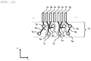
- FIG. 12 is another configuration example (hereinafter, referred to as a fourth embodiment) of the periphery of the pads 3 and the through hole forming region 13 for solving the problem of the second comparative example.
- the wiring pattern 6 connected to a part of the ground pads 3 and the ground through hole 5 connected to the wiring pattern 6 in the first embodiment are not provided.
- the wiring pattern 6 d , the ground through hole 5 d , and the ground through hole 5 d ′ connected to the ground pad 3 d in FIG. 4 are not provided.
- the through hole 5 of each differential signal pair is provided such that the through hole 5 of the other differential signal pair is located on a perpendicular bisector of a line segment connecting two differential signal through holes 5 of one of the two adjacent differential signal pairs.
- the differential signal through hole 5 c is located on a perpendicular bisector of a line segment connecting the differential signal through hole 5 e and the differential signal through hole 5 f (these three through holes 5 constitute the vertexes of a same equilateral triangle in this example).
- the reason why the through hole 5 of the other differential signal pair is located on the perpendicular bisector of the two differential signal through holes 5 of one differential signal pair is that an electromagnetic effect from the two through holes (effects of potential and magnetic field strength caused by the two through holes) is small on the plane including the perpendicular bisector of the two differential signal through holes 5 of the differential signal pair.
Landscapes
- Engineering & Computer Science (AREA)
- Microelectronics & Electronic Packaging (AREA)
- Physics & Mathematics (AREA)
- Electromagnetism (AREA)
- Structure Of Printed Boards (AREA)
- Production Of Multi-Layered Print Wiring Board (AREA)
Abstract
Description
Claims (10)
Applications Claiming Priority (1)
| Application Number | Priority Date | Filing Date | Title |
|---|---|---|---|
| PCT/JP2017/044746 WO2019116468A1 (en) | 2017-12-13 | 2017-12-13 | Wiring board and electronic device |
Publications (2)
| Publication Number | Publication Date |
|---|---|
| US20200260570A1 US20200260570A1 (en) | 2020-08-13 |
| US11229115B2 true US11229115B2 (en) | 2022-01-18 |
Family
ID=66820069
Family Applications (1)
| Application Number | Title | Priority Date | Filing Date |
|---|---|---|---|
| US16/758,463 Active US11229115B2 (en) | 2017-12-13 | 2017-12-13 | Wiring board and electronic device |
Country Status (3)
| Country | Link |
|---|---|
| US (1) | US11229115B2 (en) |
| JP (1) | JP6844035B2 (en) |
| WO (1) | WO2019116468A1 (en) |
Families Citing this family (1)
| Publication number | Priority date | Publication date | Assignee | Title |
|---|---|---|---|---|
| US12495497B2 (en) * | 2022-03-22 | 2025-12-09 | Intel Corporation | Low power memory module |
Citations (14)
| Publication number | Priority date | Publication date | Assignee | Title |
|---|---|---|---|---|
| US6462423B1 (en) * | 2000-08-31 | 2002-10-08 | Micron Technology, Inc. | Flip-chip with matched lines and ground plane |
| US6787710B2 (en) * | 2001-05-29 | 2004-09-07 | Mitsubishi Denki Kabushiki Kaisha | Wiring board and a method for manufacturing the wiring board |
| US20050201065A1 (en) | 2004-02-13 | 2005-09-15 | Regnier Kent E. | Preferential ground and via exit structures for printed circuit boards |
| US6972380B2 (en) * | 2003-01-31 | 2005-12-06 | Brocade Communications Systems, Inc. | Printed wiring board having impedance-matched differential pair signal traces |
| US20060185890A1 (en) * | 2005-02-22 | 2006-08-24 | Litton Uk Limited | Air void via tuning |
| JP2007142307A (en) | 2005-11-22 | 2007-06-07 | Hitachi Ltd | Multi-layer substrate for high-speed differential signal, communication device and data storage device |
| JP2007522679A (en) | 2004-02-13 | 2007-08-09 | モレックス インコーポレーテッド | Preferential via extension structure with triplet configuration for printed circuit boards |
| US7361846B2 (en) * | 2004-05-12 | 2008-04-22 | Siliconware Precision Industries Co., Ltd. | High electrical performance semiconductor package |
| US8183466B2 (en) * | 2004-11-29 | 2012-05-22 | Fci | Matched-impedance connector footprints |
| US20130214397A1 (en) | 2012-02-21 | 2013-08-22 | Fujitsu Limited | Multilayer wiring board and electronic device |
| US20140293566A1 (en) | 2013-03-28 | 2014-10-02 | Fujitsu Limited | Circuit board and electronic device |
| WO2015068225A1 (en) | 2013-11-06 | 2015-05-14 | 株式会社日立製作所 | Signal transmission circuit and printed circuit board |
| US20150357760A1 (en) | 2014-06-09 | 2015-12-10 | Hirose Electric Co., Ltd. | Method and apparatus for reducing far-end crosstalk in electrical connectors |
| US20180070439A1 (en) * | 2016-03-08 | 2018-03-08 | Amphenol Corporation | Backplane footprint for high speed, high density electrical connectors |
-
2017
- 2017-12-13 US US16/758,463 patent/US11229115B2/en active Active
- 2017-12-13 WO PCT/JP2017/044746 patent/WO2019116468A1/en not_active Ceased
- 2017-12-13 JP JP2019559467A patent/JP6844035B2/en active Active
Patent Citations (19)
| Publication number | Priority date | Publication date | Assignee | Title |
|---|---|---|---|---|
| US6462423B1 (en) * | 2000-08-31 | 2002-10-08 | Micron Technology, Inc. | Flip-chip with matched lines and ground plane |
| US6787710B2 (en) * | 2001-05-29 | 2004-09-07 | Mitsubishi Denki Kabushiki Kaisha | Wiring board and a method for manufacturing the wiring board |
| US6972380B2 (en) * | 2003-01-31 | 2005-12-06 | Brocade Communications Systems, Inc. | Printed wiring board having impedance-matched differential pair signal traces |
| JP2007522679A (en) | 2004-02-13 | 2007-08-09 | モレックス インコーポレーテッド | Preferential via extension structure with triplet configuration for printed circuit boards |
| US20050201065A1 (en) | 2004-02-13 | 2005-09-15 | Regnier Kent E. | Preferential ground and via exit structures for printed circuit boards |
| US7361846B2 (en) * | 2004-05-12 | 2008-04-22 | Siliconware Precision Industries Co., Ltd. | High electrical performance semiconductor package |
| US8183466B2 (en) * | 2004-11-29 | 2012-05-22 | Fci | Matched-impedance connector footprints |
| US20060185890A1 (en) * | 2005-02-22 | 2006-08-24 | Litton Uk Limited | Air void via tuning |
| US20070130555A1 (en) | 2005-11-22 | 2007-06-07 | Hitachi, Ltd. | Multilayer printed circuit board for high-speed differential signal, communication apparatus, and data storage apparatus |
| JP2007142307A (en) | 2005-11-22 | 2007-06-07 | Hitachi Ltd | Multi-layer substrate for high-speed differential signal, communication device and data storage device |
| US20130214397A1 (en) | 2012-02-21 | 2013-08-22 | Fujitsu Limited | Multilayer wiring board and electronic device |
| JP2013172036A (en) | 2012-02-21 | 2013-09-02 | Fujitsu Ltd | Multilayer wiring board and electronic apparatus |
| US20140293566A1 (en) | 2013-03-28 | 2014-10-02 | Fujitsu Limited | Circuit board and electronic device |
| JP2014192416A (en) | 2013-03-28 | 2014-10-06 | Fujitsu Ltd | Wiring board and electronic device |
| WO2015068225A1 (en) | 2013-11-06 | 2015-05-14 | 株式会社日立製作所 | Signal transmission circuit and printed circuit board |
| US20150370748A1 (en) | 2013-11-06 | 2015-12-24 | Hitachi, Ltd. | Signal transmission circuit and printed circuit board |
| US20150357760A1 (en) | 2014-06-09 | 2015-12-10 | Hirose Electric Co., Ltd. | Method and apparatus for reducing far-end crosstalk in electrical connectors |
| JP2016006874A (en) | 2014-06-09 | 2016-01-14 | ヒロセ電機株式会社 | Method and apparatus for reducing far-end crosstalk in electrical connectors |
| US20180070439A1 (en) * | 2016-03-08 | 2018-03-08 | Amphenol Corporation | Backplane footprint for high speed, high density electrical connectors |
Non-Patent Citations (2)
| Title |
|---|
| International Search Report (PCT/ISA/210) issued in PCT Application No. PCT/JP2017/044746 dated Mar. 20, 2018 with English translation (five pages). |
| Japanese-language Written Opinion (PCT/ISA/237) issued in PCT Application No. PCT/JP2017/044746 dated Mar. 20, 2018 (three pages). |
Also Published As
| Publication number | Publication date |
|---|---|
| WO2019116468A1 (en) | 2019-06-20 |
| US20200260570A1 (en) | 2020-08-13 |
| JPWO2019116468A1 (en) | 2020-06-11 |
| JP6844035B2 (en) | 2021-03-17 |
Similar Documents
| Publication | Publication Date | Title |
|---|---|---|
| US9560741B2 (en) | Circuit board via configurations for high frequency signaling | |
| CN102265708B (en) | High data rate connector system | |
| CN109076700B (en) | Backplane footprint for high-speed, high-density electrical connectors | |
| US8771018B2 (en) | Card edge connector | |
| US8545273B1 (en) | Electrical connector | |
| JP2018110087A (en) | Connector with shielding shield plate | |
| TWI618315B (en) | Connector system impedance matching | |
| US9554455B2 (en) | Method and apparatus for reducing far-end crosstalk in electrical connectors | |
| US8748753B2 (en) | Printed circuit board | |
| TWI715101B (en) | Circuit device and riser card | |
| US9548551B1 (en) | DIMM connector region vias and routing | |
| US9788419B2 (en) | Edge fingers of multi-layer printed circuit board | |
| CN104125705B (en) | Anti-loss grounding pattern structure of welding pad area of flexible circuit board | |
| JP2014509447A (en) | Controlled impedance flexible circuit | |
| US20140285280A1 (en) | Grounding pattern structure for high-frequency connection pad of circuit board | |
| US9924595B2 (en) | Cable for alternative interconnect attachement | |
| CN103269562A (en) | Filtering device applied to circuit board | |
| TWI605736B (en) | Loss-resistance structure of a high-frequency signal connection pad of a plug-in assembly | |
| US11229115B2 (en) | Wiring board and electronic device | |
| US20210392743A1 (en) | Twisted differential compensation for routing high-speed signals near power delivery inductors and system miniaturization | |
| US12107612B2 (en) | Wireless transmission system and control method | |
| US20170256874A1 (en) | Electronic circuit card with connector edge having alternated tx and rx pins assignment | |
| TWM661471U (en) | Lead assembly, electrical connector, and electronic system | |
| US9444165B2 (en) | Pin arrangement and electronic assembly | |
| CN110611990A (en) | Printed circuit board combination and electronic device using said printed circuit board combination |
Legal Events
| Date | Code | Title | Description |
|---|---|---|---|
| FEPP | Fee payment procedure |
Free format text: ENTITY STATUS SET TO UNDISCOUNTED (ORIGINAL EVENT CODE: BIG.); ENTITY STATUS OF PATENT OWNER: LARGE ENTITY |
|
| STPP | Information on status: patent application and granting procedure in general |
Free format text: NON FINAL ACTION MAILED |
|
| STPP | Information on status: patent application and granting procedure in general |
Free format text: RESPONSE TO NON-FINAL OFFICE ACTION ENTERED AND FORWARDED TO EXAMINER |
|
| STPP | Information on status: patent application and granting procedure in general |
Free format text: FINAL REJECTION MAILED |
|
| STPP | Information on status: patent application and granting procedure in general |
Free format text: RESPONSE AFTER FINAL ACTION FORWARDED TO EXAMINER |
|
| STPP | Information on status: patent application and granting procedure in general |
Free format text: ADVISORY ACTION MAILED |
|
| AS | Assignment |
Owner name: HITACHI, LTD., JAPAN Free format text: ASSIGNMENT OF ASSIGNORS INTEREST;ASSIGNORS:CHUJO, NORIO;UEMATSU, YUTAKA;YAGYU, MASAYOSHI;SIGNING DATES FROM 20200319 TO 20210907;REEL/FRAME:057540/0873 |
|
| STPP | Information on status: patent application and granting procedure in general |
Free format text: DOCKETED NEW CASE - READY FOR EXAMINATION |
|
| STPP | Information on status: patent application and granting procedure in general |
Free format text: NOTICE OF ALLOWANCE MAILED -- APPLICATION RECEIVED IN OFFICE OF PUBLICATIONS |
|
| STPP | Information on status: patent application and granting procedure in general |
Free format text: PUBLICATIONS -- ISSUE FEE PAYMENT VERIFIED |
|
| STCF | Information on status: patent grant |
Free format text: PATENTED CASE |
|
| AS | Assignment |
Owner name: HITACHI VANTARA, LTD., JAPAN Free format text: COMPANY SPLIT;ASSIGNOR:HITACHI, LTD.;REEL/FRAME:069518/0761 Effective date: 20240401 |
|
| MAFP | Maintenance fee payment |
Free format text: PAYMENT OF MAINTENANCE FEE, 4TH YEAR, LARGE ENTITY (ORIGINAL EVENT CODE: M1551); ENTITY STATUS OF PATENT OWNER: LARGE ENTITY Year of fee payment: 4 |