US11228013B2 - Anisotropic nanorod-applied light-emitting diode and light-emitting device including the same - Google Patents
Anisotropic nanorod-applied light-emitting diode and light-emitting device including the same Download PDFInfo
- Publication number
- US11228013B2 US11228013B2 US16/165,691 US201816165691A US11228013B2 US 11228013 B2 US11228013 B2 US 11228013B2 US 201816165691 A US201816165691 A US 201816165691A US 11228013 B2 US11228013 B2 US 11228013B2
- Authority
- US
- United States
- Prior art keywords
- light
- electrode
- emitting diode
- transfer layer
- layer
- Prior art date
- Legal status (The legal status is an assumption and is not a legal conclusion. Google has not performed a legal analysis and makes no representation as to the accuracy of the status listed.)
- Active
Links
Images


Classifications
-
- H—ELECTRICITY
- H10—SEMICONDUCTOR DEVICES; ELECTRIC SOLID-STATE DEVICES NOT OTHERWISE PROVIDED FOR
- H10H—INORGANIC LIGHT-EMITTING SEMICONDUCTOR DEVICES HAVING POTENTIAL BARRIERS
- H10H20/00—Individual inorganic light-emitting semiconductor devices having potential barriers, e.g. light-emitting diodes [LED]
- H10H20/80—Constructional details
- H10H20/81—Bodies
- H10H20/816—Bodies having carrier transport control structures, e.g. highly-doped semiconductor layers or current-blocking structures
- H10H20/8162—Current-blocking structures
-
- H01L51/5072—
-
- H—ELECTRICITY
- H10—SEMICONDUCTOR DEVICES; ELECTRIC SOLID-STATE DEVICES NOT OTHERWISE PROVIDED FOR
- H10K—ORGANIC ELECTRIC SOLID-STATE DEVICES
- H10K50/00—Organic light-emitting devices
- H10K50/10—OLEDs or polymer light-emitting diodes [PLED]
- H10K50/11—OLEDs or polymer light-emitting diodes [PLED] characterised by the electroluminescent [EL] layers
- H10K50/115—OLEDs or polymer light-emitting diodes [PLED] characterised by the electroluminescent [EL] layers comprising active inorganic nanostructures, e.g. luminescent quantum dots
-
- H—ELECTRICITY
- H10—SEMICONDUCTOR DEVICES; ELECTRIC SOLID-STATE DEVICES NOT OTHERWISE PROVIDED FOR
- H10H—INORGANIC LIGHT-EMITTING SEMICONDUCTOR DEVICES HAVING POTENTIAL BARRIERS
- H10H20/00—Individual inorganic light-emitting semiconductor devices having potential barriers, e.g. light-emitting diodes [LED]
- H10H20/80—Constructional details
- H10H20/81—Bodies
- H10H20/816—Bodies having carrier transport control structures, e.g. highly-doped semiconductor layers or current-blocking structures
-
- H01L51/0007—
-
- H01L51/502—
-
- H01L51/56—
-
- H—ELECTRICITY
- H10—SEMICONDUCTOR DEVICES; ELECTRIC SOLID-STATE DEVICES NOT OTHERWISE PROVIDED FOR
- H10H—INORGANIC LIGHT-EMITTING SEMICONDUCTOR DEVICES HAVING POTENTIAL BARRIERS
- H10H20/00—Individual inorganic light-emitting semiconductor devices having potential barriers, e.g. light-emitting diodes [LED]
- H10H20/01—Manufacture or treatment
-
- H—ELECTRICITY
- H10—SEMICONDUCTOR DEVICES; ELECTRIC SOLID-STATE DEVICES NOT OTHERWISE PROVIDED FOR
- H10H—INORGANIC LIGHT-EMITTING SEMICONDUCTOR DEVICES HAVING POTENTIAL BARRIERS
- H10H20/00—Individual inorganic light-emitting semiconductor devices having potential barriers, e.g. light-emitting diodes [LED]
- H10H20/80—Constructional details
- H10H20/81—Bodies
- H10H20/819—Bodies characterised by their shape, e.g. curved or truncated substrates
- H10H20/82—Roughened surfaces, e.g. at the interface between epitaxial layers
-
- H—ELECTRICITY
- H10—SEMICONDUCTOR DEVICES; ELECTRIC SOLID-STATE DEVICES NOT OTHERWISE PROVIDED FOR
- H10H—INORGANIC LIGHT-EMITTING SEMICONDUCTOR DEVICES HAVING POTENTIAL BARRIERS
- H10H20/00—Individual inorganic light-emitting semiconductor devices having potential barriers, e.g. light-emitting diodes [LED]
- H10H20/80—Constructional details
- H10H20/83—Electrodes
- H10H20/831—Electrodes characterised by their shape
-
- H—ELECTRICITY
- H10—SEMICONDUCTOR DEVICES; ELECTRIC SOLID-STATE DEVICES NOT OTHERWISE PROVIDED FOR
- H10H—INORGANIC LIGHT-EMITTING SEMICONDUCTOR DEVICES HAVING POTENTIAL BARRIERS
- H10H20/00—Individual inorganic light-emitting semiconductor devices having potential barriers, e.g. light-emitting diodes [LED]
- H10H20/80—Constructional details
- H10H20/84—Coatings, e.g. passivation layers or antireflective coatings
-
- H—ELECTRICITY
- H10—SEMICONDUCTOR DEVICES; ELECTRIC SOLID-STATE DEVICES NOT OTHERWISE PROVIDED FOR
- H10H—INORGANIC LIGHT-EMITTING SEMICONDUCTOR DEVICES HAVING POTENTIAL BARRIERS
- H10H29/00—Integrated devices, or assemblies of multiple devices, comprising at least one light-emitting semiconductor element covered by group H10H20/00
- H10H29/10—Integrated devices comprising at least one light-emitting semiconductor component covered by group H10H20/00
- H10H29/14—Integrated devices comprising at least one light-emitting semiconductor component covered by group H10H20/00 comprising multiple light-emitting semiconductor components
- H10H29/142—Two-dimensional arrangements, e.g. asymmetric LED layout
-
- H—ELECTRICITY
- H10—SEMICONDUCTOR DEVICES; ELECTRIC SOLID-STATE DEVICES NOT OTHERWISE PROVIDED FOR
- H10K—ORGANIC ELECTRIC SOLID-STATE DEVICES
- H10K50/00—Organic light-emitting devices
- H10K50/10—OLEDs or polymer light-emitting diodes [PLED]
- H10K50/14—Carrier transporting layers
- H10K50/16—Electron transporting layers
-
- H—ELECTRICITY
- H10—SEMICONDUCTOR DEVICES; ELECTRIC SOLID-STATE DEVICES NOT OTHERWISE PROVIDED FOR
- H10K—ORGANIC ELECTRIC SOLID-STATE DEVICES
- H10K71/00—Manufacture or treatment specially adapted for the organic devices covered by this subclass
-
- H—ELECTRICITY
- H10—SEMICONDUCTOR DEVICES; ELECTRIC SOLID-STATE DEVICES NOT OTHERWISE PROVIDED FOR
- H10K—ORGANIC ELECTRIC SOLID-STATE DEVICES
- H10K71/00—Manufacture or treatment specially adapted for the organic devices covered by this subclass
- H10K71/10—Deposition of organic active material
- H10K71/12—Deposition of organic active material using liquid deposition, e.g. spin coating
- H10K71/15—Deposition of organic active material using liquid deposition, e.g. spin coating characterised by the solvent used
-
- H01L2251/303—
-
- H01L2251/5353—
-
- H01L2251/5369—
-
- H01L2251/552—
-
- H01L2251/556—
-
- H01L2251/558—
-
- H01L27/3244—
-
- H01L51/5004—
-
- H—ELECTRICITY
- H10—SEMICONDUCTOR DEVICES; ELECTRIC SOLID-STATE DEVICES NOT OTHERWISE PROVIDED FOR
- H10K—ORGANIC ELECTRIC SOLID-STATE DEVICES
- H10K2101/00—Properties of the organic materials covered by group H10K85/00
- H10K2101/30—Highest occupied molecular orbital [HOMO], lowest unoccupied molecular orbital [LUMO] or Fermi energy values
-
- H—ELECTRICITY
- H10—SEMICONDUCTOR DEVICES; ELECTRIC SOLID-STATE DEVICES NOT OTHERWISE PROVIDED FOR
- H10K—ORGANIC ELECTRIC SOLID-STATE DEVICES
- H10K2101/00—Properties of the organic materials covered by group H10K85/00
- H10K2101/40—Interrelation of parameters between multiple constituent active layers or sublayers, e.g. HOMO values in adjacent layers
-
- H—ELECTRICITY
- H10—SEMICONDUCTOR DEVICES; ELECTRIC SOLID-STATE DEVICES NOT OTHERWISE PROVIDED FOR
- H10K—ORGANIC ELECTRIC SOLID-STATE DEVICES
- H10K2102/00—Constructional details relating to the organic devices covered by this subclass
-
- H—ELECTRICITY
- H10—SEMICONDUCTOR DEVICES; ELECTRIC SOLID-STATE DEVICES NOT OTHERWISE PROVIDED FOR
- H10K—ORGANIC ELECTRIC SOLID-STATE DEVICES
- H10K2102/00—Constructional details relating to the organic devices covered by this subclass
- H10K2102/301—Details of OLEDs
- H10K2102/321—Inverted OLED, i.e. having cathode between substrate and anode
-
- H—ELECTRICITY
- H10—SEMICONDUCTOR DEVICES; ELECTRIC SOLID-STATE DEVICES NOT OTHERWISE PROVIDED FOR
- H10K—ORGANIC ELECTRIC SOLID-STATE DEVICES
- H10K2102/00—Constructional details relating to the organic devices covered by this subclass
- H10K2102/301—Details of OLEDs
- H10K2102/331—Nanoparticles used in non-emissive layers, e.g. in packaging layer
-
- H—ELECTRICITY
- H10—SEMICONDUCTOR DEVICES; ELECTRIC SOLID-STATE DEVICES NOT OTHERWISE PROVIDED FOR
- H10K—ORGANIC ELECTRIC SOLID-STATE DEVICES
- H10K2102/00—Constructional details relating to the organic devices covered by this subclass
- H10K2102/301—Details of OLEDs
- H10K2102/351—Thickness
-
- H—ELECTRICITY
- H10—SEMICONDUCTOR DEVICES; ELECTRIC SOLID-STATE DEVICES NOT OTHERWISE PROVIDED FOR
- H10K—ORGANIC ELECTRIC SOLID-STATE DEVICES
- H10K2102/00—Constructional details relating to the organic devices covered by this subclass
- H10K2102/301—Details of OLEDs
- H10K2102/361—Temperature
-
- H—ELECTRICITY
- H10—SEMICONDUCTOR DEVICES; ELECTRIC SOLID-STATE DEVICES NOT OTHERWISE PROVIDED FOR
- H10K—ORGANIC ELECTRIC SOLID-STATE DEVICES
- H10K50/00—Organic light-emitting devices
- H10K50/10—OLEDs or polymer light-emitting diodes [PLED]
- H10K50/11—OLEDs or polymer light-emitting diodes [PLED] characterised by the electroluminescent [EL] layers
-
- H—ELECTRICITY
- H10—SEMICONDUCTOR DEVICES; ELECTRIC SOLID-STATE DEVICES NOT OTHERWISE PROVIDED FOR
- H10K—ORGANIC ELECTRIC SOLID-STATE DEVICES
- H10K59/00—Integrated devices, or assemblies of multiple devices, comprising at least one organic light-emitting element covered by group H10K50/00
- H10K59/10—OLED displays
- H10K59/12—Active-matrix OLED [AMOLED] displays
Definitions
- the present disclosure relates to a light-emitting diode, and more particularly, to a light-emitting diode having improved luminescence properties and a light-emitting device including the same.
- an organic light-emitting diode (OLED) display device and a quantum dot light-emitting diode (QLED) display device can have a thin film structure and low power consumption, and thus, have attracted attention as next-generation display devices that replace liquid crystal display (LCD) devices.”
- OLED organic light-emitting diode
- QLED quantum dot light-emitting diode
- LCD liquid crystal display
- Light emitting diodes such as OLEDs or QLEDs are diodes in which, when charges are injected into an emissive layer formed between an electron injection electrode (cathode) and a hole injection electrode (anode), electron-hole pairs are formed and then annihilated, thereby emitting light.
- the light-emitting diode includes an anode and a cathode, which are disposed opposite to each other, an emitting material layer (EML) disposed between the anode and the cathode, a hole injection layer (HIL) and a hole transport layer (HTL), which are disposed between the anode and the EML, and an electron transport layer (ETL) disposed between the cathode and the EML.
- EML emitting material layer
- HIL hole injection layer
- HTL hole transport layer
- EML electron transport layer
- the EML comprises a light-emitting material, and holes and electrons, which are injected from the anode and the cathode, respectively, are combined in the EML, thereby forming excitons. Due to such energy, the light-emitting material included in the EML is in an excited state, in an organic compound, energy transition from the excited state to a ground state occurs, and the energy generated thereby is emitted as light.
- each layer should be formed of materials having a suitable bandgap energy.
- the HIL may be formed of poly(3,4-ethylenedioxythiophene) polystyrene sulfonate (PEDOT:PSS), the HTL may be formed of poly(4-butylphenyl-diphenyl-amine) (Poly-TPD), and ETL may be formed of an organic material such as 2-biphenyl-4-yl-5-(4-t-butylphenyl)-1,3,4-oxadiazole (PBD).
- PDA poly(3,4-ethylenedioxythiophene) polystyrene sulfonate
- PTD poly(4-butylphenyl-diphenyl-amine)
- PBD 2-biphenyl-4-yl-5-(4-t-butylphenyl)-1,3,4-oxadiazole
- a lowest unoccupied molecular orbital (LUMO) energy level of the organic material used in the ETL is considerably higher than a conduction band energy level of the cathode. Since a difference between the conduction band energy level of the cathode and the LUMO energy level of the ETL is considerably large, an energy barrier is created between the cathode and the ETL, and thus the injection of electrons produced in the cathode into the ETL is delayed.
- LUMO lowest unoccupied molecular orbital
- the present disclosure is directed to a light-emitting diode, a process for forming a light emitting diode and a light-emitting device that obviate one or more of the problems due to limitations and disadvantages of the related art.
- Embodiment of the present disclosure are to provide a light-emitting diode having improved charge mobility by reducing charge trap sites while driving, a method of forming a charge transfer layer constituting the light-emitting diode, and a light-emitting device having the light-emitting diode.
- the present disclosure further provides a light-emitting diode having improved luminescence properties, a method of forming a charge transfer layer constituting the light-emitting diode, and a light-emitting device having the light-emitting diode.
- the present disclosure provides a light-emitting diode, which includes an electron transfer layer between electrodes that are disposed opposite to each other, wherein the electron transfer layer comprises anisotropic nanorods, and the long axis of the anisotropic nanorod is arranged at an angle of about 20 to about 90° (degrees) with respect to the interface between the electron transfer layer and a layer adjacent to the electron transfer layer.
- the present disclosure provides a method of forming an electron transfer layer of the light-emitting diode, the method including: coating a substrate prepared previously with a dispersion containing anisotropic nanorods in a solvent, and stacking an electron transfer layer including the anisotropic nanorods on the substrate by baking the solution applied to the substrate, wherein the stacking of the electron transfer layer is performed by pre-baking the substrate at a temperature of about 5 to about 50° C. lower than a boiling point of the solvent for about 5 to about 30 minutes and post-baking the substrate at a temperature ranging from the boiling point of the solvent to a temperature of about 20° C. higher than the boiling point of the solvent for about 20 to about 30 minutes.
- the present disclosure provides a light-emitting device, for example, a light-emitting display device, which has the above-described light-emitting diode.
- FIG. 1 is a cross-sectional view schematically illustrating a structure of a light-emitting diode according to a first exemplary embodiment of the present disclosure, in which anisotropic nanorods are applied to an electron transfer layer;
- FIG. 2 is a schematic diagram illustrating that, compared with the use of isotropic nanodot-shaped inorganic particles as a material constituting an electron transfer layer, the use of anisotropic nanorod-type inorganic particles according to the present disclosure contributes to reduced electron trap sites, leading to an enhanced electron transfer distance and improved electron mobility;
- FIG. 3 is a flowchart schematically illustrating a process of forming an electron transfer layer according to an exemplary embodiment of the present disclosure, to which anisotropic nanorod-type inorganic particles whose long axes are arranged at a predetermined angle with respect to the interface with an adjacent emissive layer, which constitutes a light-emitting diode, are applied;
- FIG. 4 is a cross-sectional view schematically illustrating a structure of a light-emitting diode according to a second exemplary embodiment of the present disclosure, in which anisotropic nanorods are applied to an electron transfer layer;
- FIG. 5 is a cross-sectional view schematically illustrating a structure of a light-emitting diode display device as an example of a light-emitting device to which the light-emitting diode according to the present disclosure is applied;
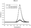
- FIGS. 6 to 9 are graphs of voltage (V)-luminescence, voltage-current density, electroluminescence (EL) spectra, and the maximum luminescence for anisotropic nanorod-type inorganic particles having different aspect ratios (AR) in an electron transfer layer according to the present disclosure, respectively.
- samples represented by only ZnO mean that isotropic nanodot-shaped ZnO is used;
- FIGS. 10A to 10G are electron microscope images each illustrating that the long axes of anisotropic nanorod-type inorganic particles are arranged at a predetermined angle with respect to an interface with a substrate according to an exemplary embodiment of the present disclosure.
- FIG. 11 is a graph of luminescence according to an angle between the long axis of anisotropic nanorod-type inorganic particles and an interface with a substrate according to an exemplary embodiment of the present disclosure.
- NR represents that anisotropic nanorods are used.
- FIG. 1 is a cross-sectional view schematically illustrating a light-emitting diode having a normal structure according to a first exemplary embodiment of the present disclosure.
- the light-emitting diode 100 according to the first exemplary embodiment of the present disclosure includes a first electrode 110 , a second electrode 120 disposed opposite to the first electrode 110 , and an emissive layer 130 disposed between the first electrode 110 and the second electrode 120 and including an EML 150 .
- the emissive layer 130 may further include a first charge transfer layer 140 between the first electrode 110 and the EML 150 , and a second charge transfer layer 160 between the EML 150 and the second electrode 120 .
- the first electrode 110 may be an anode such as a hole injection electrode.
- the first electrode 110 may be formed on a substrate which is formed of glass or a polymer.
- the first electrode 110 may be a doped or undoped metal oxide such as indium-tin-oxide (ITO), indium-zinc-oxide (IZO), indium-tin-zinc-oxide (ITZO), indium-copper-oxide (ICO), tin oxide (SnO 2 ), indium oxide (In 2 O 3 ), cadmium:zinc oxide (Cd:ZnO), fluorine:tin oxide (F:SnO 2 ), indium:zinc oxide (In:SnO 2 ), gallium:tin oxide (Ga:SnO 2 ) or aluminum:zinc oxide (Al:ZnO; AZO).
- ITO indium-tin-oxide
- IZO indium-zinc-oxide
- ITZO indium-tin-zinc-
- the first electrode 110 may comprise a metal or non-metal material, other than the above-described metal oxide, for instance, nickel (Ni), platinum (Pt), gold (Au), silver (Ag), iridium (Ir) or a carbon nanotube (CNT).
- a metal or non-metal material other than the above-described metal oxide, for instance, nickel (Ni), platinum (Pt), gold (Au), silver (Ag), iridium (Ir) or a carbon nanotube (CNT).
- the second electrode 120 may be a cathode such as an electron injection electrode.
- the second electrode 120 may comprise Ca, Ba, Ca/Al, LiF/Ca, LiF/Al, BaF 2 /Al, CsF/Al, CaCO 3 /Al, BaF 2 /Ca/Al, Al, Mg, Au:Mg or Ag:Mg.
- each of the first electrode 110 and the second electrode 120 may be stacked to a thickness of 30 to 300 nm.
- the first electrode 110 may comprise a transparent conductive metal such as ITO, IZO, ITZO or AZO, and as the second electrode 120 , Ca, Ba, Ca/Al, LiF/Ca, LiF/Al, BaF 2 /Al, Al, Mg, or an Ag:Mg alloy may be used.
- a transparent conductive metal such as ITO, IZO, ITZO or AZO
- the second electrode 120 Ca, Ba, Ca/Al, LiF/Ca, LiF/Al, BaF 2 /Al, Al, Mg, or an Ag:Mg alloy may be used.
- the first charge transfer layer 140 that can constitute the emissive layer 130 is disposed between the first electrode 110 and the EML 150 .
- the first charge transfer layer 140 may be a hole transfer layer which provides holes to the EML 150 .
- the first charge transfer layer 140 includes a HIL 142 disposed adjacent to the first electrode 110 between the first electrode 110 and the EML 150 , and an HTL 144 disposed adjacent to the EML 150 between the first electrode 110 and the EML 150 .
- the HIL 142 facilitates the injection of holes, from the first electrode 110 , into the EML 150 .
- the HIL 142 may comprise an organic material selected from the group consisting of poly(ethylenedioxythiophene):polystyrenesulfonate (PEDOT:PSS); tetrafluoro-tetracyano-quinodimethane (F4-TCNQ)-doped 4,4′,4′′-tris(diphenylamino)triphenylamine (TDATA), for example, a p-doped phthalocyanine such as F4-TCNQ-doped zinc phthalocyanine (ZnPc), F4-TCNQ-doped N,N′-diphenyl-N,N′-bis(1-naphthyl)-1,1′-biphenyl-4,4′′-diamine ( ⁇ -NPD); hexaazatriphenylene-hexanitrile (HAT-CN
- the dopant such as F4-TCNQ may be doped at a ratio of 1 to 30 wt % with respect to the weight of a host.
- the HIL 142 may be omitted according to the structure and type of the light-emitting diode 100 .
- the HTL 144 transfers holes from the first electrode 110 to the EML 150 .
- the HTL 144 may comprise an inorganic material or an organic material.
- the HTL 144 may be formed of an organic material selected from the group consisting of arylamines such as 4,4′-N,N′-dicarbazolyl-biphenyl (CBP), N,N′-diphenyl-N,N′-bis(1-naphtyl)-1,1′-biphenyl-4,4′′-diamine ( ⁇ -NPD), N,N′-diphenyl-N,N′-bis(3-methylphenyl)-(1,1′-biphenyl)-4,4′-diamine (TPD), N,N′-bis(3-methylphenyl)-N,N′-bis(phenyl)-spiro (spiro-TPD), N,N′-di(4-(N,N′-dip
- the HTL 144 may be formed of an inorganic material selected from the group consisting of a metal oxide such as NiO, MoO 3 , Cr 2 O 3 , Bi 2 O 3 or p-type ZnO; a non-oxide equivalent such as copper thiocyanate (CuSCN), Mo 2 S, or p-type GaN; and a combination thereof.
- a metal oxide such as NiO, MoO 3 , Cr 2 O 3 , Bi 2 O 3 or p-type ZnO
- a non-oxide equivalent such as copper thiocyanate (CuSCN), Mo 2 S, or p-type GaN
- the first charge transfer layer 140 is divided into the HIL 142 and the HTL 144 , the first charge transfer layer 140 may be formed as a monolayer.
- the HIL 142 may be omitted, the first charge transfer layer 140 may comprise only the HTL 144 , or the above-described hole transport organic material may be doped with the hole injection material (e.g., PEDOT:PSS).
- the hole injection material e.g., PEDOT:PSS
- the first charge transfer layer 140 including the HIL 142 and the HTL 144 may be formed by one selected from a vacuum deposition process including vacuum vapor deposition and sputtering, and a solution process such as spin coating, drop coating, dip coating, spray coating, roll coating, flow coating, and casting, screen printing and inkjet printing, or a combination thereof.
- a vacuum deposition process including vacuum vapor deposition and sputtering
- a solution process such as spin coating, drop coating, dip coating, spray coating, roll coating, flow coating, and casting, screen printing and inkjet printing, or a combination thereof.
- thicknesses of the HIL 142 and the HTL 144 may range from 10 to 200 nm, and preferably 10 to 100 nm, but the present disclosure is not limited thereto.
- the EML 150 may consist of inorganic luminescent particles or an organic light-emitting material.
- the inorganic luminescent particles may comprise inorganic light-emitting nanoparticles such as quantum dots (QDs) or quantum rods (QRs).
- QDs or QRs are inorganic particles that emit light while electrons in an unstable state drop from a conduction band to a valence band.
- These inorganic light-emitting nanoparticles have a very high extinction coefficient and excellent quantum yield among inorganic particles, and thus generate strong fluorescence.
- an emission wavelength varies according to the size of inorganic light-emitting nanoparticles, when the size of inorganic light-emitting nanoparticles is adjusted, light in the entire visible light region may be obtained, thereby realizing a variety of colors.
- the color purity of each pixel may be increased, and white light consisting of red (R), green (G) and blue (B) light with high purity may be realized.
- each of the QDs or QRs may have a single structure.
- the QDs or QRs may have a heterologous core/shell structure.
- the shell may comprise one shell, or multi-shells.
- reaction temperature of synthesizing the core and/or shell a ligand typ, and reactivity and the injection rates of reaction precursors constituting the core and/or the shell, a growth degree, a crystal structure and the like of these inorganic light-emitting nanoparticles may be adjusted, and therefore, light emission in various wavelengths according to the adjustment of an energy bandgap may be induced.
- each of the QDs or QRs may have a heterologous structure, which comprises a core component disposed in the center of the QD or QR for emitting light, and a shell surrounding the surface of the core to protect the core, and ligand components may surround the surface of the shell to disperse the QDs or QRs in a solvent.
- each of the QDs or QRs may have a type-I core/shell structure in which the energy bandgap of the component of the core is surrounded by the energy bandgap of the shell, and electrons and holes are transferred to the core and recombined in the core, which is a luminous body, thereby emitting energy as light.
- the core is a part in which luminescence substantially occurs, and the emission wavelength of the QDs or QRs is determined according to a core size.
- the core has a smaller size than the exciton Bohr radius according to a material and an optical bandgap at the corresponding size.
- the shell constituting the QDs or QRs promotes the quantum confinement effect of the core and determines the stability of the QDs or QRs.
- Atoms exposed at the surface of single-structured colloidal QDs or QRs unlike internal atoms, have lone pair electrons which do not participate in a chemical bond. The energy level of these surface atoms is between the conduction band edge and the valence band edge of the QDs or QRs to trap the charges, thereby forming surface defects.
- the luminous efficiency of the QDs or QRs may be reduced, and the chemical composition of the QDs or QRs may be modified by the reaction between the trapped charges and external oxygen and compound, or electrical/optical properties of the QDs or QRs may be permanently lost.
- the QDs or QRs may have the heterologous structure of a core/a shell.
- the lattice constant of a material constituting the shell should be similar to that of a material constituting the core.
- the oxidation of the core may be prevented, thereby enhancing the chemical stability of the QDs or QRs, minimizing the loss of excitons caused by the surface trap on the surface of the core, preventing the loss of energy by molecular vibration, and thus enhancing quantum yield.
- the QDs or QRs may be semiconductor nanocrystals or metal oxide particles having a quantum confinement effect.
- the QDs or QRs may include Group II-VI, III-V, IV-VI, or nano semiconductor compounds.
- the core and/or shell constituting the QDs or QRs may be Group II-VI compound semiconductor nanocrystals such as CdS, CdSe, CdTe, ZnS, ZnSe, ZnTe, HgS, HgTe and/or a combination thereof; Group III-V compound semiconductor nanocrystals such as GaP, GaAs, GaSb, InP, InAs, InSb and/or a combination thereof; Group IV-VI compound semiconductor nanocrystals such as PbS, PbSe, PbTe and/or a combination thereof; Group compound semiconductor nanocrystals such as AgGaS 2 , AgGaSe 2 , AgGaTe 2 , CuInS 2 , CuInSe 2 ,
- the semiconductor nanoparticle may be undoped or doped with a rare earth element such as Eu, Er, Tb, Tm or Dy or an arbitrary combination thereof, or doped with a transition metal element such as Mn, Cu, Ag or Al or an arbitrary combination thereof.
- a rare earth element such as Eu, Er, Tb, Tm or Dy or an arbitrary combination thereof
- a transition metal element such as Mn, Cu, Ag or Al or an arbitrary combination thereof.
- the core constituting the QDs or QRs may be selected from the group consisting of ZnSe, ZnTe, CdSe, CdTe, InP, ZnCdS, Cu x In 1-x S, Cu x In 1-x Se, Ag x In 1-x S and a combination thereof.
- the shell constituting the QDs or QRs may be selected from the group consisting of ZnS, GaP, CdS, ZnSe, CdS/ZnS, ZnSe/ZnS, ZnS/ZnSe/CdSe, GaP/ZnS, CdS/CdZnS/ZnS, ZnS/CdSZnS, Cd X Zn 1-x S and a combination thereof.
- the QDs may be alloy QDs (e.g., CdS x Se 1-x , CdSe x Te 1-x , and Zn x Cd 1-x Se) such as homogeneous alloy QDs or gradient alloy QDs.
- the EML 150 comprises inorganic luminescent particles such as QDs or QRs
- the EML 150 is formed by applying a solution containing the QDs or QRs in a solvent on the first charge transfer layer 140 , for example, an HTL 144 , using a solution process, and volatilizing the solvent.
- the EML 150 may be formed by applying a dispersion containing the QDs or QRs in a solvent on the first charge transfer layer 140 through a solution process, and volatilizing the solvent.
- the EML 150 may be formed using one selected from the solution processes such as spin coating, drop coating, dip coating, spray coating, roll coating, flow coating casting, screen printing and inkjet printing, or a combination thereof.
- the EML 150 may include inorganic light-emitting nanoparticles, QDs or QRs, having photoluminescence (PL) properties at 440 nm, 530 nm, and 620 nm, thereby manufacturing a white light-emitting diode.
- the EML 150 may include luminescent particles such as QDs or QRs having any one of red, green and blue colors, and may be formed to individually emit any one color.
- the EML 150 may comprise an organic light-emitting material.
- the EML 150 comprise an organic light-emitting material
- any conventional organic light-emitting material is used without particular limitation.
- the EML 150 may comprise an organic light-emitting material(s) emitting red, green and/or blue light, and may include a fluorescent light-emitting material or a phosphorescent light-emitting material.
- the organic light-emitting material constituting the EML 150 may include a host and a dopant.
- the dopant may be doped at about 1 to about 50 wt %, and preferably about 1 to about 30 wt %, with respect to the host weight, but the present disclosure is not limited thereto.
- the organic host used in the EML 150 may be any material which is conventionally used, but the present disclosure is not particularly limited thereto.
- the organic host used in the EML 150 may comprise tris(8-hydroxyquinoline)aluminum (Alq 3 ), TCTA, PVK, 4,4′-bis(N-carbazolyl)-1,1′-biphenyl (CBP), 4,4′-bis(9-carbazolyl)-2,2′-dimethylbiphenyl (CDBP), 9,10-di(naphthalene-2-yl)anthracene (ADN), 3-tert-butyl-9,10-di(naphtha-2-yl)anthracene (TBADN), 2-methyl-9,10-bis(naphthalene-2-yl)anthracene (MADN), 1,3,5-tris(N-phenylbenzimidazole-2-yl)benzene (TPBi), distyrylarylene (
- the dopant included in the EML 150 may be an organic compound or organic metal complex such as 5,6,11,12-tetraphenylnaphthalene (rubrene), bis(2-benzo[b]-thiophene-2-yl-pyridine)(acetylacetonate)iridium (III) (Ir(btp) 2 (acac)), bis[1-(9,9-diemthyl-9H-fluoren-2-yl)-isoquinoline](acetylacetonate)iridium (III) (Ir(fliq) 2 (acac)), bis[2-(9,9-diemthyl-9H-fluoren-2-yl)-quinoline](acetylacetonate)iridium (III) (Ir(flq) 2 (acac)), bis-(2-phenylquinoline)(2-(3-methylphenyl)pyridinate)iridium (III)
- an organic compound or organic metal complex
- the dopant included in the EML 150 may be, but is not limited to, an organic compound or organic metal complex such as N,N′-dimethyl-quinacridone (DMQA), coumarin 6, 9,10-bis[N,N-di-(p-tolyl)-amino]anthracene (TTPA), 9,10-bis[phenyl(m-tolyl)-amino]anthracene (TPA), bis(2-phenylpyridine)(acetylacetonate)iridium (III) (Ir(ppy) 2 (acac)), fac-tris(phenylpyridine)iridium (III) (fac-Ir(ppy) 3 ), or tris[2-(p-tolyl)pyridine]iridium (III) (Ir(mppy) 3 ).
- DMQA N,N′-dimethyl-quinacridone
- TTPA 9,10-bis[N,N-di-(p-tolyl)-amin
- the dopant included in the EML 150 may be, but is not limited to, an organic compound or organic metal complex such as 4,4′-bis[4-(di-p-tolylamino)styryl]biphenyl (DPAVBi), perylene, 2,5,8,11-tetra-tert-butylpherylene (TBPe), bis(3,5-difluoro-2-(2-pyridyl)phenyl-(2-carbozylpyridyl)iridium (III) (FirPic), mer-tris(1-phenyl-3-methylimidazolin-2ylidene-C,C2′) iridium (III) (mer-Ir(pmi) 3 ), or tris(2-(4,6-difluorophenyl)pyridine)iridium (III) (Ir(Fppy) 3 ).
- an organic compound or organic metal complex such as 4,4′-bis[4-(di-p-to
- the EML 150 may be formed by one selected from vacuum deposition processes including vacuum vapor deposition and sputtering, and solution processes including spin coating, drop coating, dip coating, spray coating, roll coating, and flow coating, cast, screen printing, and inkjet printing, or a combination thereof.
- vacuum deposition processes including vacuum vapor deposition and sputtering
- solution processes including spin coating, drop coating, dip coating, spray coating, roll coating, and flow coating, cast, screen printing, and inkjet printing, or a combination thereof.
- the second charge transfer layer 160 is disposed between the EML 150 and the second electrode 120 .
- the second charge transfer layer 160 may be an electron transfer layer which provides electrons to the EML 150 .
- the second charge transfer layer 160 may include an electron injection layer (EIL) 162 disposed adjacent to the second electrode 120 between the second electrode 120 and the EML 150 , and an ETL 164 disposed adjacent to the EML 150 between the second electrode 120 and the EML 150 .
- EIL electron injection layer
- the EIL 162 facilitates injection of electrons from the second electrode 120 into the EML 150 .
- the EIL 162 may comprise a material in which a metal such as Al, Cd, Cs, Cu, Ga, Ge, In or Li is doped or bound with fluorine, or a metal oxide (e.g., titanium dioxide (TiO 2 ), zinc oxide (ZnO), zirconium oxide (ZrO), tin oxide (SnO 2 ), tungsten oxide (WO 3 ) or tantalum oxide (Ta 2 O 3 )) which is undoped or doped with Al, Mg, In, Li, Ga, Cd, Cs, Cu or the like.
- a metal oxide e.g., titanium dioxide (TiO 2 ), zinc oxide (ZnO), zirconium oxide (ZrO), tin oxide (SnO 2 ), tungsten oxide (WO 3 ) or tantalum oxide (Ta 2 O 3 )
- the ETL 164 is configured to transport electrons to the EML 150 .
- the ETL 164 may comprise inorganic particles such as anisotropic nanorods 170 .
- the inorganic particles have a deeper valence band (VB) energy level than a HOMO or valence band (VB) energy level of the light-emitting material used in the EML 150 . Therefore, holes injected into the EML 150 from the first electrode 110 are blocked in the ETL 164 consisting of an inorganic material having a very deep VB energy level, and thus, hole leakage to the second electrode 120 may be blocked.
- a conduction band (CB) energy level of the ETL 164 comprising an inorganic material is similar to that of the second electrode 120 . Since there is no energy barrier between the second electrode 120 and the ETL 164 , electrons generated in the second electrode 120 may be rapidly injected into the EML 150 via the ETL 164 comprising an inorganic material.
- CB conduction band
- the average diameter of the nanodots is merely several nanometers, but the ETL 164 is generally stacked to a thickness of tens of nanometers.
- the contact points at the particle-particle interface serve as trap sites of charges such as electrons.
- the ETL 164 is formed of isotropic nanodots, there is a very high probability of trapping electrons at many contact points between the isotropic nanodots. Therefore, when an isotropic nanodot-type inorganic material is used for the ETL 164 , electron injection may be delayed.
- the interface between particles is smaller than that of the nanodots at the same volume, and thus contact points between the particles are reduced. That is, when anisotropic nanorod-type inorganic particles are used for the ETL 164 , compared with the use of the isotropic nanodot-type inorganic particles, the contact points between the particles are reduced. For this reason, charge trap sites are also reduced, and thus an electron injection velocity (electron mobility) and an electron drift distance may increase. Accordingly, when the anisotropic nanorod-type inorganic particles are used for the ETL 164 , electron injection efficiency may be improved, resulting in improvement in luminous efficiency.
- the anisotropic nanorod 170 that can be used for the ETL 164 has a long axis 172 and a short axis 174 .
- the aspect ratio (AR) of the long axis 172 to the short axis 174 of the anisotropic nanorod 170 may range from about 2:1 to about 4:1.
- the electron trap sites are reduced and thus electron mobility is improved, and as a result, a light-emitting diode 100 having improved luminescence properties such as current density or luminescence may be realized.
- anisotropic nanorod 170 -type metal oxide particles may be prepared by hydrothermal synthesis or vapor phase growth.
- the length of the long axis 172 may range from approximately 4 to 40 run, and the length of the short length 174 may range from 2 to 10 nm, but the present disclosure is not limited thereto.
- the long axis 172 of the anisotropic nanorod 170 constituting the ETL 164 according to the present disclosure may be arranged at a predetermined angle ( 0 ) with respect to an interface with an adjacent layer into which electrons are injected or from which electrons are emitted (e.g., the second electrode 120 or the EIL 162 in a second exemplary embodiment of the present disclosure).
- the long axis 172 of the anisotropic nanorod 170 is arranged as perpendicular as possible to the interface with the electron-injected adjacent layer, trap sites of the anisotropic nanorods 170 for the electrons injected into the ETL 164 are reduced, electron mobility is improved, and an electron drift distance is also increased. Therefore, in the ETL 164 , the velocity and efficiency of injecting electrons to the EML 150 may be improved, and thus the luminescence properties of the light-emitting diode 100 may be improved.
- the long axes 172 of the anisotropic nanorods 170 may be arranged at an angle ranging from about 20 to about 90 degrees, preferably 30 to 90 degrees, and more preferably 50 to 90 degrees with respect to the electron-injected interface. It is preferable to control baking conditions in a solution process in order to arrange the long axes 172 of the anisotropic nanorods 170 as perpendicular as possible to the electron-injected interface, and the control of baking conditions will be described below.
- a metal oxide that has excellent electron mobility, allows holes and electrons to be injected into the EML 150 in equilibrium, and has excellent efficiency of the recombination of injected charges may be used.
- the inorganic material for the anisotropic nanorod 170 may be a metal oxide selected from, but are not limited to, the group consisting of zinc oxide (ZnO), zinc magnesium oxide (ZnMgO), titanium dioxide (TiO 2 ), magnesium oxide (MgO), zirconium dioxide (ZrO 2 ), tin oxide (SnO), tin dioxide (SnO 2 ), tungsten oxide (WO 3 ), tantalum oxide (Ta 2 O 3 ), hafnium oxide (HfO 3 ), aluminum oxide (Al 2 O 3 ), zirconium silicon oxide (ZrSiO 4 ), barium titanium oxide (BaTiO 3 ), and barium zirconium oxide (BaZrO 3 ) and combination thereof.
- the anisotropic nanorod 170 -type metal oxide particles may be undoped, or doped with Al, Mg, In, Li, Ga, Cd, Cs, Cu or the like.
- FIG. 1 illustrates that the second charge transfer layer 160 as a bilayer of the EIL 162 and the ETL 164 , the second charge transfer layer 160 may be formed as a monolayer of the ETL 164 .
- the second charge transfer layer 160 may be formed as a single layer of the ETL 164 formed of a blend of cesium carbonate with the above-described electron-transporting inorganic material.
- the second charge transfer layer 160 including the EIL 162 and/or the ETL 164 may be formed using one selected from solution processes such as spin coating, drop coating, dip coating, spray coating, roll coating, flow coating, casting, screen printing and inkjet printing, or a combination thereof.
- each of the EIL 162 and the ETL 164 may be stacked to a thickness of 10 to 200 nm, and preferably 10 to 100 nm.
- the luminescence properties of the light-emitting diode 100 may be enhanced.
- CTL hybrid charge transfer layer
- the light-emitting diode 100 may include at least one exciton blocking layer adjacent to the EML 150 .
- the light-emitting diode 100 may have an electron blocking layer (EBL) capable of controlling and preventing the transfer of electrons between the HTL 144 and the EML 150 .
- EBL electron blocking layer
- the EBL may comprise TCTA, tris[4-(diethylamino)phenyl]amine), N-(biphenyl-4-yl)-9,9-dimethyl-N-(4-(9-phenyl-9H-carbazole-3-yl)phenyl)-9H-fluoren-2-amine, tri-p-tolylamine, 1,1-bis(4-(N,N-di(p-tolyl)amino)phenyl)cyclohexane (TAPC), m-MTDATA, 1,3-bis(N-carbazolyl)benzene (mCP), 3,3′-bis(N-carbazolyl)-1,1′-biphenyl (mCBP), poly-TPD, copper phthalocyanine (CuPc), DNTPD and/or 1,3,5-tris[4-(diphenylamino)phenyl]benzene (TDAPB).
- TCTA tris[4-(diethy
- a hole blocking layer (HBL), as a second exciton blocking layer, may be disposed between the EML 150 and the ETL 164 , thereby preventing the transfer of holes between the EML 150 and the ETL 164 .
- HBL hole blocking layer
- a derivative of an oxadiazole-based compound, a triazole-based compound, a phenanthroline-based compound, a benzoxazole-based compound, a benzothiazole-based compound, a benzimidazole-based compound, a triazine-based compound or the like may be used as a material for the HBL.
- the HBL may comprise 2,9-dimethyl-4,7-diphenyl-1,10-phenanthroline (BCP), BAlq, Alq 3 , PBD, spiro-PBD and/or 8-hydroxy-quinolinato lithium (LIQ), which have/has a deeper highest occupied molecular orbital (HOMO) energy level than that of the material used for the EML 150 .
- BCP 2,9-dimethyl-4,7-diphenyl-1,10-phenanthroline
- BAlq Alq 3
- PBD spiro-PBD
- LIQ 8-hydroxy-quinolinato lithium
- the ETL 164 disposed between the EML 150 and the second electrode 120 is formed of anisotropic nanorod 170 -type inorganic particles.
- the long axes of the anisotropic nanorods 170 are arranged as perpendicular as possible to the electron-injected interface.
- the method of forming the ETL 160 constituting the light-emitting diode includes preparing a substrate (S 310 ), coating the substrate with a dispersion containing the anisotropic nanorods 170 (see FIG. 1 ) (S 320 ) and baking the anisotropic nanorod-containing dispersion applied onto the substrate (S 330 ).
- the substrate onto which the dispersion containing the anisotropic nanorods 170 (see FIG. 1 ) is applied may be the EML 150 (see FIG. 1 ).
- a substrate onto which a dispersion containing anisotropic nanorods 170 is applied may be a first electrode 210 (see FIG. 4 ) or an EIL 242 (see FIG. 4 ).
- a solvent that can disperse the anisotropic nanorods 170 is not particularly limited.
- a solvent that disperses the anisotropic nanorods 170 may be an orthogonal solvent that does not disperse a light-emitting material constituting the EML 150 adjacent to the ETL 164 .
- an emitting material may be blended with a solution for forming the ETL 164 , and thus the boundary between the EML 150 and the ETL 164 may not be clearly distinguished. As a result, the luminescence properties of the light-emitting diode 100 may be degraded.
- a solvent capable of dispersing the anisotropic nanorods 170 may be a C 1 to C 5 alcohol, ethylene glycol, propylene glycol, dimethyl sulfoxide and a combination thereof.
- a C 1 to C 5 alcohol such as methanol, ethanol, isopropyl alcohol and/or butanol, which have (has) an excellent dispersion property with respect to anisotropic metal oxide particles, may be used as a dispersion solvent.
- the application method may be, but is not particularly limited to, one selected from the solution processes such as spin coating, drop coating, dip coating, spray coating, roll coating, flow coating casting, screen printing and inkjet printing, or a combination thereof.
- the dispersion containing the anisotropic nanorods 170 in a solvent may be applied onto the substrate by performing spin coating at 1000 to 5000 rpm, and preferably 1500 to 4000 rpm.
- the baking of the solution applied onto the substrate (S 330 ) according to the present disclosure may include pre-baking and post-baking.
- the forming of the ETL 164 including the anisotropic nanorods 170 on the substrate may include pre-baking at a temperature of about 5 to about 50° C., and preferably, about 10 to about 50° C. lower than the boiling point of the solvent constituting the solution coated on the substrate for about 5 to about 30 minutes, and post-baking at the boiling point to a temperature of about 20° C. higher than the boiling point of the solvent for about 20 to about 30 minutes.
- the long axes 172 of the anisotropic nanorod 170 may be arranged.
- the long axes 172 of the anisotropic nanorods 170 may be arranged as perpendicular as possible to an electron-injected interface, for example, at an angle of about 20 to about 90 degrees, preferably, about 25 to about 90 degrees, more preferably, about 30 to about 90 degrees, and the most preferably, about 50 to about 90 degrees.
- the pre-baking may include pre-baking the solution coated on the substrate at a temperature of about 30 to about 50° C. lower than the boiling point of the solvent for about 5 to about 20 minutes, and preferably, about 10 to about 20 minutes as a first step, and after the first pre-baking, pre-baking at a temperature of about 10 to about 30° C., and preferably, about 20 to about 30° C. lower than the boiling point of the solvent for about 10 to about 20 minutes as a second step.
- the long axes 172 of the anisotropic nanorods 170 may be arranged as perpendicular as possible, for example, at an angle of about 50 to about 90 degrees, with respect to the electron-injected interface.
- the light-emitting diode having a normal structure in which an HTL is disposed between a first electrode having a relatively low work function and an EML, and an electron transfer layer is disposed between a second electrode having a relatively high work function and an EML has been described with reference to FIG. 2 .
- the light-emitting diode may alternatively have an inverted structure, other than the normal structure, and this case will be described with reference to FIG. 4 .
- FIG. 4 is a cross-sectional view schematically illustrating a light-emitting diode having an inverted structure according to a secondary exemplary embodiment of the present disclosure.
- the light-emitting diode 200 according to the second exemplary embodiment of the present disclosure includes a first electrode 210 , a second electrode 220 disposed opposite to the first electrode 210 , and an emissive layer 230 disposed between the first electrode 210 and the second electrode 220 and including an EML 250 .
- the emissive layer 230 may further include a first charge transfer layer 240 disposed between the first electrode 210 and the EML 250 , and a second charge transfer layer 260 disposed between the second electrode 220 and the EML 250 .
- the first electrode 210 may be a cathode such as an electron injection electrode.
- first electrode 210 may comprise a doped or undoped metal oxide such as ITO, IZO, ITZO, ICO, SnO 2 , In 2 O 3 , Cd:ZnO, F:SnO 2 , In:SnO 2 , Ga:SnO 2 and AZO, or of a material containing Ni, Pt, Au, Ag, Ir or a CNT, other than the above-described metal oxides.
- the second electrode 220 may be an anode such as a hole injection electrode.
- the second electrode 220 may be Ca, Ba, Ca/Al, LiF/Ca, LiF/Al, BaF 2 /Al, CsF/Al, CaCO 3 /Al, BaF 2 /Ca/Al, Al, Mg, Au:Mg or Ag:Mg.
- each of the first electrode 210 and the second electrode 220 may be stacked to a thickness of 30 nm to 300 nm.
- the first charge transfer layer 240 may be an electron transfer layer that supplies electrons to the EML 250 .
- the first charge transfer layer 240 includes an EIL 242 between the first electrode 210 and the EML 250 such that the EIL 242 is located adjacent to the first electrode 210 , and an ETL 244 between the first electrode 210 and the EML 250 such that the ETL 244 is located adjacent to the EML 250 .
- the EIL 242 may be formed of a material obtained by doping a metal such as Al, Cd, Cs, Cu, Ga, Ge, In, or Li with fluorine or binding such a metal to fluorine; or a metal oxide such as TiO 2 , ZnO, ZrO, SnO 2 , WO 3 , or Ta 2 O 3 that is undoped or doped with Al, Mg, In, Li, Ga, Cd, Cs, Cu, or the like.
- a metal such as Al, Cd, Cs, Cu, Ga, Ge, In, or Li
- a metal oxide such as TiO 2 , ZnO, ZrO, SnO 2 , WO 3 , or Ta 2 O 3 that is undoped or doped with Al, Mg, In, Li, Ga, Cd, Cs, Cu, or the like.
- the ETL 244 may be formed of anisotropic nanorod 170 -type inorganic particles.
- the inorganic particles may be metal oxide particles having excellent electron mobility.
- the anisotropic nanorod 170 may have a long axis 172 and a short axis 174 , and the aspect ratio of the long axis 172 to the short axis 174 may range from about 2:1 to about 4:1.
- the long axes 172 of the anisotropic nanorods 170 may be arranged at an angle ( ⁇ ) of about 20 to about 90 degrees with respect to an electron-injected interface (e.g., an interface with the first electrode 210 or the EIL 242 ).
- the first charge transfer layer 240 may be formed only as a monolayer of the ETL 244 .
- the first charge transfer layer 240 may be formed as a monolayer of the ETL 244 formed by blending cesium carbonate with the above-described electron-transporting inorganic material consisting of the above-described anisotropic nanorod 170 -type inorganic particles.
- each of the EIL 242 and the ETL 244 may be stacked to a thickness of 10 to 200 nm, and preferably 10 to 100 nm.
- the EML 250 may be formed of inorganic luminescent particles or an organic light-emitting material.
- the inorganic luminescent particles may be inorganic light-emitting nanoparticles such as QDs or QRs.
- the QDs or QRs may have a single structure, or a heterologous core/shell structure.
- the QDs or QRs may be semiconductor nanocrystals or metal oxide particles having a quantum confinement effect.
- the QDs or QRs may include Group II-VI, III-V, IV-VI, or nano semiconductor compounds.
- the core and/or shell constituting the QDs or QRs may be Group II-VI compound semiconductor nanocrystals such as CdS, CdSe, CdTe, ZnS, ZnSe, ZnTe, HgS, HgTe and/or a combination thereof; Group III-V compound semiconductor nanocrystals such as GaP, GaAs, GaSb, InP, InAs, InSb and/or a combination thereof; Group IV-VI compound semiconductor nanocrystals such as PbS, PbSe, PbTe and/or a combination thereof; Group compound semiconductor nanocrystals such as AgGaS 2 , AgGaSe 2 , AgGaTe 2 , CuInS 2 , CuInSe 2 ,
- the semiconductor nanoparticle may be undoped or doped with a rare earth element such as Eu, Er, Tb, Tm or Dy or an arbitrary combination thereof, or doped with a transition metal element such as Mn, Cu, Ag or Al or an arbitrary combination thereof.
- a rare earth element such as Eu, Er, Tb, Tm or Dy or an arbitrary combination thereof
- a transition metal element such as Mn, Cu, Ag or Al or an arbitrary combination thereof.
- the EML 250 comprises inorganic luminescent particles such as QDs or QRs
- the EML 250 is formed by applying a solution containing the QDs or QRs in a solvent on the first charge transfer layer 240 , for example, an HTL 244 , using a solution process, and volatilizing the solvent.
- the EML 250 may be formed of an organic light-emitting material(s) emitting red light, green light and/or blue light, and may further include a fluorescence-emitting material or a phosphorescence-emitting material.
- the organic light-emitting material constituting the EML 250 may include a host and a dopant.
- the dopant may be doped at 1 to 50 wt %, and preferably 1 to 30 wt %, with respect to the host weight, but the present disclosure is not limited thereto.
- the EML 250 may be formed by one selected from vacuum deposition processes including vacuum vapor deposition and sputtering, and solution processes including spin coating, drop coating, dip coating, spray coating, roll coating, flow coating, cast, screen printing, and inkjet printing, or a combination thereof.
- the second charge transfer layer 260 may be an hole transfer layer which provides holes to the EML 250 .
- the second charge transfer layer 260 may include an HIL 262 disposed adjacent to the second electrode 220 between the second electrode 220 and the EML 250 , and an HTL 264 disposed adjacent to the EML 250 between the second electrode 220 and the EML 250 .
- the HIL 262 may be formed of a material selected from the group consisting of PEDOT:PSS, F4-TCNQ-doped TDATA, for example, a p-doped phthalocyanine such as F4-TCNQ-doped ZnPc, F4-TCNQ-doped ⁇ -NPD, HAT-CN and a combination thereof, but the present disclosure is not limited thereto.
- a dopant such as F4-TCNQ may be used for doping of a host at a quantity of 1 to 30 wt % with respect to the weight of a host.
- the HIL 262 may be omitted according to the structure and type of the light-emitting diode 200 .
- the HTL 264 may comprise an inorganic material or an organic material.
- the HTL 264 may comprise an organic material selected from the group consisting of arylamines such as CBP, ⁇ -NPD, TPD, spiro-TPD, DNTPD, TCTA, m-MTDATA, TFB and poly-TPD; polyaniline; a polypyrrole; poly(para)phenylenevinylenes such as PPV, MEH-PPV and MOMO-PPV and derivatives thereof copper phthalocyanine; aromatic tertiary amines or polynuclear tertiary amines; 4,4′-bis(p-carbazolyl)-1,1′-biphenyl compounds; N,N,N′,N′-tetraarylbenzidine; PEDOT:PSS and derivatives thereof poly-N-vinylcarbazole and derivatives thereof polymethacrylate and derivatives thereof; poly(9,9-octylfluorene)
- the HTL 264 may comprise an inorganic material selected from the group consisting of metal oxides such as NiO, MoO 3 , Cr 2 O 3 , Bi 2 O 3 and p-type ZnO; non-oxidized equivalents such as copper thiocyanate (CuSCN), Mo 2 S, and p-type GaN; and a combination thereof.
- metal oxides such as NiO, MoO 3 , Cr 2 O 3 , Bi 2 O 3 and p-type ZnO
- non-oxidized equivalents such as copper thiocyanate (CuSCN), Mo 2 S, and p-type GaN
- CuSCN copper thiocyanate
- the second charge transfer layer 260 may be formed as a monolayer.
- the second charge transfer layer 260 may comprise only the HTL 264 without the HIL 262 , or may be prepared by doping the above-described hole-transporting organic material with a hole injection material (e.g., PEDOT:PSS). Thicknesses of the HIL 262 and the HTL 264 may range from 10 to 200 nm, and preferably 10 to 100 nm, but the present disclosure is not limited thereto.
- the light-emitting diode 200 may include at least one exciton blocking layer disposed adjacent to the EML 250 .
- the light-emitting diode 200 may further include an EBL disposed between the EML 250 and the HTL 264 to control and prevent the transfer of electrons, and an HBL disposed between the ETL 244 and the EML 250 to control and prevent the transfer of holes.
- the ETL 244 disposed between the first electrode 210 and the EML 250 is formed of an inorganic material such as a metal oxide. Holes generated in the second electrode 220 and then injected into the EML 250 may be blocked in the ETL 244 formed of an inorganic material having a deep VB energy level.
- the ETL 244 may comprise anisotropic nanorods 170 , and long axes 172 of the anisotropic nanorods 170 are arranged as perpendicular as possible with respect to an electron-injected interface. As trap sites of electrons injected into the ETL 244 are reduced, electron mobility is improved, and an electron drift distance increases. Accordingly, the efficiency and velocity of electron injection into the EML 250 are enhanced, and thus the luminescence properties of the light-emitting diode 200 may be improved.
- the electron transfer-induced light-emitting diode comprising anisotropic nanorod-type inorganic particles having a long axis arranged at a predetermined angle with respect to an electron-injected interface may be applied to a light-emitting device such as a lighting device or a display device.
- a light-emitting device including a light-emitting diode in which anisotropic nanorod-type inorganic particles are applied to an ETL according to the present disclosure will be described.
- FIG. 5 is a cross-sectional view schematically illustrating a light-emitting display device according to an exemplary embodiment of the present disclosure.
- the light-emitting display device 300 includes a substrate 310 , a driving thin film transistor Tr, which is a driving element, disposed on the substrate 310 , and a light-emitting diode 400 connected to the driving thin film transistor Tr.
- a semiconductor layer 322 comprising an oxide semiconductor material or polycrystalline silicon is formed on the substrate 310 .
- the semiconductor layer 322 comprise an oxide semiconductor material
- a light shielding pattern (not shown) may be formed under the semiconductor layer 322 to prevent light from being incident upon the semiconductor layer 322 , thus preventing degradation of the semiconductor layer 322 due to light.
- the semiconductor layer 322 may comprise polycrystalline silicon, and in this case, opposite edges of the semiconductor layer 322 may be doped with impurities.
- a gate insulating film 324 comprising an insulating material is formed on the semiconductor layer 322 .
- the gate insulating film 324 may comprise an inorganic insulating material such as silicon oxide (SiO 2 ) or silicon nitride (SiNx).
- a gate electrode 330 comprising a conductive material such as a metal is formed on the gate insulating film 324 to correspond to the center of the semiconductor layer 322 .
- the interlayer insulating film 332 consisting of an insulating material is formed on the gate electrode 330 .
- the interlayer insulating film 332 may be formed of an inorganic insulating material such as silicon oxide (SiO 2 ) or silicon nitride (SiNx), or an organic insulating material such as benzocyclobutene or photo-acryl.
- the interlayer insulating film 332 has first and second semiconductor layer contact holes 334 and 336 exposing two opposite sides of the semiconductor layer 322 .
- the first and second semiconductor layer contact holes 334 and 336 are disposed on two opposite sides of the gate electrode 330 such that they are spaced apart from the gate electrode 330 .
- a source electrode 340 and a drain electrode 342 which comprise a conductive material such as a metal, are formed on the interlayer insulating film 332 .
- the source electrode 340 and the drain electrode 342 are disposed on the respective side of the gate electrode 330 such that they are spaced apart with respect to the center of the gate electrode 330 , and are connected to two opposite sides of the semiconductor layer 322 via the first and second semiconductor layer contact holes 334 and 336 , respectively.
- the semiconductor layer 322 , the gate electrode 330 , the source electrode 340 , and the drain electrode 342 constitute the driving thin film transistor Tr, which is a driving element.
- the driving thin film transistor Tr has a coplanar structure in which the gate electrode 330 , the source electrode 340 and the drain electrode 342 are disposed on the semiconductor layer 322 .
- the driving thin film transistor Tr may have an inverted staggered structure in which a gate electrode is disposed under the semiconductor layer, and a source electrode and a drain electrode are disposed on the semiconductor layer.
- the semiconductor layer may comprise amorphous silicon.
- pixel areas are defined by gate lines and data lines that cross one another, and a switching element connected to the gate line and the data line is further provided.
- the switching element is connected to the driving thin film transistor Tr, which is a driving element.
- a power line disposed spaced apart from and parallel to the gate line or data line, and a storage capacitor may be further included to constantly maintain a voltage of the gate electrode of the driving thin film transistor Tr, which is a driving element, during one frame.
- a passivation layer 350 having a drain contact hole 352 through which the drain electrode 342 of the driving thin film transistor Tr is exposed is formed in such a way that it covers the driving thin film transistor Tr.
- the passivation layer 350 may be formed of an inorganic insulating material such as a silicon oxide (SiO 2 ) or a silicon nitride (SiNx), or an organic insulating material such as benzocyclobutene or photo-acryl.
- the light-emitting diode 400 is disposed on the passivation layer 350 .
- a first electrode 410 connected to the drain electrode 342 of the driving thin film transistor Tr though the drain contact hole 352 is formed on the passivation layer 350 so as to be divided for each pixel area.
- the first electrode 410 may be an anode or a cathode.
- the first electrode 410 may comprise a conductive material having a relatively high work function.
- the first electrode 410 may comprise a doped or undoped metal oxide such as ITO, IZO, ITZO, ICO, SnO 2 , In 2 O 3 , Cd:ZnO, F:SnO 2 , In:SnO 2 , Ga:SnO 2 or AZO, or, other than the above-mentioned metal oxides, it may comprise a metal material including nickel (Ni), platinum (Pt), gold (Au), silver (Ag), iridium (Ir) or a CNT.
- a doped or undoped metal oxide such as ITO, IZO, ITZO, ICO, SnO 2 , In 2 O 3 , Cd:ZnO, F:SnO 2 , In:SnO 2 , Ga:SnO 2 or AZO, or, other than the above-mentioned metal oxides, it may comprise a metal material including nickel (Ni), platinum (Pt), gold (Au), silver (Ag),
- a reflective electrode or a reflective layer may be further provided under the first electrode 410 .
- the reflective electrode or reflective layer may comprise an aluminum-palladium-copper (APC) alloy.
- a bank layer 368 covering an edge of the first electrode 410 is formed on the passivation layer 350 .
- the bank layer 368 is configured to expose the center of the first electrode 410 corresponding to a pixel area.
- An emissive layer 430 is formed on the first electrode 410 .
- the emissive layer 430 may consist only of an EML, or it may have multiple charge transfer layers to increase luminous efficiency.
- FIG. 5 illustrates that the emissive layer 430 comprises the first charge transfer layer 440 , the EML 450 and the second charge transfer layer 460 , which are sequentially stacked between the first electrode 410 and the second electrode 420 .
- the first charge transfer layer 440 may be a hole transfer layer, composed of an HIL 142 (see FIG. 1 ) formed of an organic material or an inorganic material and an HTL 144 (see FIG. 1 ).
- the EML 450 may comprise inorganic luminescent particles or an organic light-emitting material.
- the second charge transfer layer 460 may be an electron transfer layer, composed of an EIL 162 (see FIG. 1 ) and an ETL 164 (see FIG. 1 ).
- the second charge transfer layer 460 may include the ETL 164 (see FIG. 1 ) formed of an anisotropic nanorod 170 -type inorganic material.
- the anisotropic nanorod 170 may have a long axis 172 and a short axis 174 , in which the long axis 172 is arranged at an angle ( ⁇ ) of approximately about 20 to about 90 degrees with respect to an electron-injected interface.
- the second electrode 420 is formed on the emissive layer 430 , which is formed above a substrate 310 .
- the second electrode 420 may be a cathode or anode.
- the second electrode 420 may be disposed on the entire surface of a display region, and may be formed of a conductive material having a relatively small work function.
- the second electrode 420 may be Ca, Ba, Ca/Al, LiF/Ca, LiF/Al, BaF 2 /Al, CsF/Al, CaCO 3 /Al, BaF 2 /Ca/Al, Al, Mg, Au:Mg or Ag:Mg.
- FIG. 5 illustrates the light-emitting diode 400 having a normal structure, in which the first charge transfer layer 440 as a hole transfer layer is disposed between the first electrode 410 and the emitting material layer 450 , and the second charge transfer layer 460 as an electron transfer layer is disposed between the second electrode 420 and the emitting material layer 450 .
- the second charge transfer layer 460 disposed between the EML 450 and the second electrode 420 is formed of an inorganic material such as metal oxide having a deep VB energy level, holes injected into the EML 450 may be effectively blocked in the second charge transfer layer 460 .
- the long axes of the anisotropic nanorod 170 constituting the second charge transfer layer 460 are arranged as perpendicular as possible to an electron-injected interface. As trap sites of electrons injected into the first charge transfer layer 460 are reduced, electron mobility is improved, and an electron drift distance increases. The efficiency and velocity of electron injection into the EML 450 are enhanced, and thus the luminescence properties of the light-emitting diode 400 and the light-emitting display device 300 including the same may be improved.
- a light-emitting diode having an inverted structure in which a first charge transfer layer as an electron transfer layer is disposed between the first electrode 410 and the emitting material layer 450 , and a second charge transfer layer as a hole transfer layer is disposed between the second electrode 420 and the emitting material layer 450 may be manufactured.
- the ETL formed of an anisotropic nanorod 170 -type inorganic material may be included in the first charge transfer layer 440 disposed between the first electrode 410 and the EML 450 .
- the first charge transfer layer 440 disposed between the EML 450 and the first electrode 410 is formed of an inorganic material such as a metal oxide having a deep VB energy level, holes injected into the EML 450 may be effectively blocked in the first charge transfer layer 440 .
- the long axes of the anisotropic nanorods 170 constituting the first charge transfer layer 440 are arranged as perpendicular as possible to an electron-injected interface. As trap sites of electrons injected into the first charge transfer layer 440 are reduced, electron mobility is improved, and an electron drift distance increases. The efficiency and velocity of electron injection into the EML 450 are enhanced, and thus the luminescence properties of the light-emitting diode 400 and the light-emitting display device 300 including the same may be improved.
- Zinc oxide (ZnO) particles having an average aspect ratio (AR) of the long axis to the short axis of 2 as anisotropic nanorod-type inorganic particles were purchased commercially and applied to an ETL of a light-emitting diode. Particularly, patterning of an ITO glass was performed to have an emission area of 3 mm ⁇ 3 mm, and then washed. Subsequently, an emissive layer and a cathode were stacked according to the following order: an HIL (PEDOT:PSS, spin coating (5000 rpm) and then heating at 150° C.
- HIL PEDOT:PSS
- spin coating 5000 rpm
- an HTL spin coating (4000 rpm) of TFB (8 mg/mL in toluene), and then heating at 180° C. for 30 minutes; 20 nm), an EML (spin coating (3000 rpm) of InP-based red QDs (10 mg/mL in hexane) and then heating at 80° C. for 30 minutes; 20 nm), an ETL (spin coating of ZnO having an AR of 2 (12.5 mg/mL in ethanol), and then heating at 80° C. for 30 minutes; 20 nm).
- the substrate on which the emissive layer is formed as described above was mounted in a vacuum chamber, and a cathode (Al; 80 nm) was deposited at a base pressure of 1 ⁇ 10 ⁇ 6 Tom After deposition, for film formation, the substrate was transferred into a dry box from a deposition chamber, followed by encapsulation using UV-curable epoxy and a moisture getter. The resulting light-emitting diode has an emission area of 9 mm 2 .
- a light-emitting diode was manufactured in the same manner as described in Example 1, except that anisotropic nanorod (NR)-type ZnO particles having an AR of 3 as inorganic particles of an ETL were used.
- NR anisotropic nanorod
- a light-emitting diode was manufactured in the same manner as described in Example 1, except that anisotropic nanorod (NR)-type ZnO particles having an AR of 4 as inorganic particles of an ETL were used.
- NR anisotropic nanorod
- a light-emitting diode was manufactured in the same manner as described in Example 1, except that isotropic nanodot-type ZnO particles as inorganic particles of an ETL were used.
- Each of the light-emitting diodes manufactured according to Examples 1 to 3 and Comparative Example 1 was connected to an external power source, electroluminescence (EL) properties of all diodes manufactured in the present disclosure were evaluated at room temperature using a constant current source (KEITHLEY) and a photometer PR650. Particularly, voltage (V)-luminescence (L; nit), voltage (V)-current density (mA/cm 2 ), EL intensity and maximum luminescence of the light-emitting diodes manufactured in Examples 1 to 3 and Comparative Example 1 were measured. The measurement results are shown in Table 1 below and FIGS. 6 to 9 .
- the luminescence increased up to 6.53 times, the current density increased up to 1.34 times, and the EL intensity increased up to 7.98 times. Therefore, it was confirmed that when the anisotropic nanorod-type inorganic particles are formed in the ETL, a light-emitting diode having improved luminescence properties can be realized.
- a light-emitting diode was manufactured in the same manner as described in Example 1, except that anisotropic nanorod (NR)-type ZnO particles having an AR of 3 as inorganic particles of an ETL were applied onto an EML by spin coating, and then heating at 100° C. for 30 minutes.
- anisotropic nanorod (NR)-type ZnO particles having an AR of 3 as inorganic particles of an ETL were applied onto an EML by spin coating, and then heating at 100° C. for 30 minutes.
- a light-emitting diode was manufactured in the same manner as described in Example 1, except that anisotropic nanorod (NR)-type ZnO particles having an AR of 3 as inorganic particles of an ETL were applied onto an EML by spin coating, and then heating at 80° C. for 30 minutes.
- anisotropic nanorod (NR)-type ZnO particles having an AR of 3 as inorganic particles of an ETL were applied onto an EML by spin coating, and then heating at 80° C. for 30 minutes.
- a light-emitting diode was manufactured in the same manner as described in Example 1, except that anisotropic nanorod (NR)-type ZnO particles having an AR of 3 as inorganic particles of an ETL were applied onto an EML by spin coating and heating at 70° C. for 5 minutes and then at 80° C. for 30 minutes.
- anisotropic nanorod (NR)-type ZnO particles having an AR of 3 as inorganic particles of an ETL were applied onto an EML by spin coating and heating at 70° C. for 5 minutes and then at 80° C. for 30 minutes.
- a light-emitting diode was manufactured in the same manner as described in Example 1, except that anisotropic nanorod (NR)-type ZnO particles having an AR of 3 as inorganic particles of an ETL were applied onto an EML by spin coating and heating at 70° C. for 10 minutes and then at 80° C. for 20 minutes.
- anisotropic nanorod (NR)-type ZnO particles having an AR of 3 as inorganic particles of an ETL were applied onto an EML by spin coating and heating at 70° C. for 10 minutes and then at 80° C. for 20 minutes.
- a light-emitting diode was manufactured in the same manner as described in Example 1, except that anisotropic nanorod (NR)-type ZnO particles having an AR of 3 as inorganic particles of an ETL were applied onto an EML by spin coating and heating at 60° C. for 10 minutes and then at 80° C. for 20 minutes.
- anisotropic nanorod (NR)-type ZnO particles having an AR of 3 as inorganic particles of an ETL were applied onto an EML by spin coating and heating at 60° C. for 10 minutes and then at 80° C. for 20 minutes.
- a light-emitting diode was manufactured in the same manner as described in Example 1, except that anisotropic nanorod (NR)-type ZnO particles having an AR of 3 as inorganic particles of an ETL were applied onto an EML by spin coating and heating at 50° C. for 10 minutes, at 70° C. for 10 minutes and then at 80° C. for 20 minutes.
- anisotropic nanorod (NR)-type ZnO particles having an AR of 3 as inorganic particles of an ETL were applied onto an EML by spin coating and heating at 50° C. for 10 minutes, at 70° C. for 10 minutes and then at 80° C. for 20 minutes.
- a light-emitting diode was manufactured in the same manner as described in Example 1, except that anisotropic nanorod (NR)-type ZnO particles having an AR of 3 as inorganic particles of an ETL were applied onto an EML by spin coating and heating at 30° C. for 20 minutes, at 50° C. for 10 minutes and then at 80° C. for 20 minutes.
- anisotropic nanorod (NR)-type ZnO particles having an AR of 3 as inorganic particles of an ETL were applied onto an EML by spin coating and heating at 30° C. for 20 minutes, at 50° C. for 10 minutes and then at 80° C. for 20 minutes.
- a light-emitting diode was manufactured in the same manner as described in Example 1, except that isotropic nanodot-type ZnO particles as inorganic particles of an ETL were applied onto an EML by spin coating and heating at 80° C. for 30 minutes.
- FIGS. 10A to 10G and FIG. 11 by applying the anisotropic nanorod-type ZnO particles onto the substrate, and varying baking conditions, an ETL in which the long axes of anisotropic nanorods were arranged almost perpendicular to an electron-injected interface may be formed. As the long axes of anisotropic nanorods were arranged almost perpendicular to the electron-injected interface, the luminescence of a light-emitting diode increased.
- anisotropic nanorod-type inorganic particles are applied to an electron transfer layer.
- the anisotropic nanorods have a smaller interface with adjacent particles at the same volume. Therefore, during the transfer of electrons generated in a cathode to an EML, at the interface between the anisotropic nanorod-type inorganic particles constituting the electron transfer layer, contact points with the electrons, that is, electron trap sites, are reduced, and an electron injection property and electron mobility can be improved.
- the long axes of the anisotropic nanorods are arranged to have a predetermined angle or more with respect to an interface between the electron transport layer and an adjacent layer, for example, an EML.
- an EML Light emitted from the EML is emitted to the outside along the long axes of the nanorods arranged at a predetermined angle or more with respect to the interface, thereby improving luminescence.
- the electron transfer layer comprising the anisotropic nanorod-type inorganic particles whose long axes are arranged at a predetermined angle or more with respect to the interface with the adjacent layer is applied, a light-emitting diode and a light-emitting device, which have improved luminescence properties such as luminance, current density, etc.
Landscapes
- Physics & Mathematics (AREA)
- Optics & Photonics (AREA)
- Engineering & Computer Science (AREA)
- Chemical & Material Sciences (AREA)
- Crystallography & Structural Chemistry (AREA)
- Inorganic Chemistry (AREA)
- Nanotechnology (AREA)
- Manufacturing & Machinery (AREA)
- Electroluminescent Light Sources (AREA)
Abstract
Description
| TABLE 1 |
| EL properties of light-emitting diodes |
| mA/ | mA/ | ||||
| Sample | ETL | nit* | cm2* | cm2** | EL*** |
| Example 1 | NR (AR = 2) | 578.16 | 515.57 | 836.76 | 0.3185 |
| Example 2 | NR (AR = 3) | 693.79 | 567.12 | 920.43 | 0.03822 |
| Example 3 | NR (AR = 4) | 367.71 | — | — | — |
| Comparative | Nanodot | 106.17 | 422.26 | 793.6 | 0.004794 |
| Example 1 | |||||
| *5 V, | |||||
| **6 V, | |||||
| ***640 nm | |||||
| TABLE 2 |
| EL properties of light-emitting diodes |
| Long axis | Lumi- | |||
| arrangement | nescence | |||
| Sample | ETL | Baking | (°) | (nit) |
| Example 4 | |
100° C./30 min | Random | 326 |
| Example 5 | NR ZnO | 80° C./30 min | 15.9 | 312 |
| Example 6 | NR ZnO | 70° C./5 min → | 20.5 | 353 |
| 80° C./30 min | ||||
| Example 7 | NR ZnO | 70° C./10 min → | 29 | 378 |
| 80° C./20 min | ||||
| Example 8 | NR ZnO | 60° C./10 min → | 34.4 | 436 |
| 80° C./20 min | ||||
| Example 9 | |
50° C./10 min → | 55.8 | 623 |
| 70° C./10 min → | ||||
| 80° C./20 min | ||||
| Example 10 | NR ZnO | 30° C./20 min → | 72.3 | 746 |
| 50° C./10 min → | ||||
| 80° C./20 min | ||||
| Comparative | Dot ZnO | 80° C./30 min | — | 126 |
| Example 2 | ||||
Claims (18)
Applications Claiming Priority (2)
| Application Number | Priority Date | Filing Date | Title |
|---|---|---|---|
| KR10-2017-0136359 | 2017-10-20 | ||
| KR1020170136359A KR102420787B1 (en) | 2017-10-20 | 2017-10-20 | Light emitting diode applying anisotropic nano rod and light emitting apparatus having thereof |
Publications (2)
| Publication Number | Publication Date |
|---|---|
| US20190123292A1 US20190123292A1 (en) | 2019-04-25 |
| US11228013B2 true US11228013B2 (en) | 2022-01-18 |
Family
ID=66171260
Family Applications (1)
| Application Number | Title | Priority Date | Filing Date |
|---|---|---|---|
| US16/165,691 Active US11228013B2 (en) | 2017-10-20 | 2018-10-19 | Anisotropic nanorod-applied light-emitting diode and light-emitting device including the same |
Country Status (3)
| Country | Link |
|---|---|
| US (1) | US11228013B2 (en) |
| KR (1) | KR102420787B1 (en) |
| CN (1) | CN109698259B (en) |
Families Citing this family (9)
| Publication number | Priority date | Publication date | Assignee | Title |
|---|---|---|---|---|
| CN107833976A (en) * | 2017-10-24 | 2018-03-23 | 深圳市华星光电半导体显示技术有限公司 | The preparation method and QLED devices of QLED devices |
| EP4043533B1 (en) | 2018-08-24 | 2025-10-08 | Samsung Electronics Co., Ltd. | Light emitting device and display device including the same |
| CN113196881B (en) * | 2018-12-17 | 2024-05-14 | 夏普株式会社 | Electroluminescent element and display device |
| CN110603643A (en) * | 2019-08-07 | 2019-12-20 | 京东方科技集团股份有限公司 | Display panel, display device, light emitting element, and method of manufacturing display panel |
| KR102650052B1 (en) * | 2019-08-29 | 2024-03-25 | 한국전자통신연구원 | light emitting device and manufacturing method thereof |
| CN113161495B (en) * | 2020-01-22 | 2024-09-06 | 京东方科技集团股份有限公司 | Organic light emitting diode and display device |
| JP7162647B2 (en) * | 2020-09-15 | 2022-10-28 | Jx金属株式会社 | Cu-W-O sputtering target and oxide thin film |
| CN115312669A (en) * | 2021-05-07 | 2022-11-08 | Tcl科技集团股份有限公司 | A quantum dot electroluminescent device |
| WO2023073784A1 (en) * | 2021-10-25 | 2023-05-04 | シャープディスプレイテクノロジー株式会社 | Light emitting element and display device |
Citations (6)
| Publication number | Priority date | Publication date | Assignee | Title |
|---|---|---|---|---|
| US20070045620A1 (en) * | 2005-08-26 | 2007-03-01 | Park Jin-Woo | Dual emission organic light emitting display device and method of driving the same |
| US20110079796A1 (en) * | 2009-10-05 | 2011-04-07 | Zena Technologies, Inc. | Nano structured leds |
| US20110281070A1 (en) * | 2008-08-21 | 2011-11-17 | Innova Dynamics, Inc. | Structures with surface-embedded additives and related manufacturing methods |
| US20130038178A1 (en) * | 2011-08-08 | 2013-02-14 | Samsung Electronics Co., Ltd. | Znsno3/zno nanowire having core-shell structure, method of forming znsno3/zno nanowire and nanogenerator including znsno3/zno nanowire, and method of forming znsno3 nanowire and nanogenerator including znsno3 nanowire |
| CN103730584A (en) | 2013-12-27 | 2014-04-16 | 北京京东方光电科技有限公司 | Display panel and display device |
| US20180331312A1 (en) * | 2015-11-04 | 2018-11-15 | Guangzhou Chinaray Optoelectronic Materials Ltd. | Electroluminescent device, preparation method thereof, and ink formulation |
-
2017
- 2017-10-20 KR KR1020170136359A patent/KR102420787B1/en active Active
-
2018
- 2018-10-19 CN CN201811221683.8A patent/CN109698259B/en active Active
- 2018-10-19 US US16/165,691 patent/US11228013B2/en active Active
Patent Citations (8)
| Publication number | Priority date | Publication date | Assignee | Title |
|---|---|---|---|---|
| US20070045620A1 (en) * | 2005-08-26 | 2007-03-01 | Park Jin-Woo | Dual emission organic light emitting display device and method of driving the same |
| US20110281070A1 (en) * | 2008-08-21 | 2011-11-17 | Innova Dynamics, Inc. | Structures with surface-embedded additives and related manufacturing methods |
| US20110079796A1 (en) * | 2009-10-05 | 2011-04-07 | Zena Technologies, Inc. | Nano structured leds |
| CN102971805A (en) | 2010-02-27 | 2013-03-13 | 因努瓦动力有限公司 | Structures with surface-embedded additives and related manufacturing methods |
| US20130038178A1 (en) * | 2011-08-08 | 2013-02-14 | Samsung Electronics Co., Ltd. | Znsno3/zno nanowire having core-shell structure, method of forming znsno3/zno nanowire and nanogenerator including znsno3/zno nanowire, and method of forming znsno3 nanowire and nanogenerator including znsno3 nanowire |
| CN103730584A (en) | 2013-12-27 | 2014-04-16 | 北京京东方光电科技有限公司 | Display panel and display device |
| US20160028035A1 (en) * | 2013-12-27 | 2016-01-28 | Boe Technology Group Co., Ltd. | Display panel and display device |
| US20180331312A1 (en) * | 2015-11-04 | 2018-11-15 | Guangzhou Chinaray Optoelectronic Materials Ltd. | Electroluminescent device, preparation method thereof, and ink formulation |
Non-Patent Citations (1)
| Title |
|---|
| Shariffudin et al., "Hybrid Organic-Inorganic Light Emitting Diode using ZnO Nanorods as Electron Transport Layer", Jan. 9, 2014, IEEE, RSM 2013 IEEE Symposium on Micro and Nanoelectronics, pp. 340-343 (Year: 2014). * |
Also Published As
| Publication number | Publication date |
|---|---|
| CN109698259B (en) | 2021-09-14 |
| US20190123292A1 (en) | 2019-04-25 |
| KR20190044216A (en) | 2019-04-30 |
| CN109698259A (en) | 2019-04-30 |
| KR102420787B1 (en) | 2022-07-13 |
Similar Documents
| Publication | Publication Date | Title |
|---|---|---|
| US11653512B2 (en) | Light-emitting diode and light-emitting device with reduced hole and current leakages | |
| US10665805B2 (en) | Light-emitting diode and light-emitting device including the same | |
| JP6685362B2 (en) | Light emitting diode and light emitting device including the same | |
| US11228013B2 (en) | Anisotropic nanorod-applied light-emitting diode and light-emitting device including the same | |
| US10439155B2 (en) | Quantum dot light-emitting diode and quantum dot light-emitting device having the same | |
| US11398580B2 (en) | Light emitting diode and light emitting device including the same | |
| US11355710B2 (en) | Light-emitting diode and light-emitting device including the same | |
| US10978659B2 (en) | Inorganic illuminant, light-emitting diode and light-emitting device having thereof | |
| KR102481171B1 (en) | Light emitting diode and light emitting device having the diode | |
| US11950438B2 (en) | Inorganic light emitting diode and inorganic light emitting device including the same | |
| US11502267B2 (en) | Inorganic light emitting diode and inorganic light emitting device including the same | |
| KR102517276B1 (en) | Light emitting diode and light emitting device having the diode | |
| US11437598B2 (en) | Light emitting diode and light emitting device including the same | |
| KR20190061746A (en) | Organic compounds, lighe emitting diode and light emitting device having the compounds | |
| US11495769B2 (en) | Inorganic light emitting diode and inorganic light emitting device including the same | |
| KR20210077257A (en) | Process of manufacturing light emitting film having inorganic luminescent particle, process of light emitting device and inorganic light emitting diode having inorganic luminescnent particle |
Legal Events
| Date | Code | Title | Description |
|---|---|---|---|
| FEPP | Fee payment procedure |
Free format text: ENTITY STATUS SET TO UNDISCOUNTED (ORIGINAL EVENT CODE: BIG.); ENTITY STATUS OF PATENT OWNER: LARGE ENTITY |
|
| AS | Assignment |
Owner name: LG DISPLAY CO., LTD., KOREA, REPUBLIC OF Free format text: ASSIGNMENT OF ASSIGNORS INTEREST;ASSIGNORS:WOO, SUNG-IL;KIM, DONG-YOUNG;CHOI, HYE-OCK;SIGNING DATES FROM 20181008 TO 20181011;REEL/FRAME:047286/0841 |
|
| STPP | Information on status: patent application and granting procedure in general |
Free format text: DOCKETED NEW CASE - READY FOR EXAMINATION |
|
| STPP | Information on status: patent application and granting procedure in general |
Free format text: NON FINAL ACTION MAILED |
|
| STPP | Information on status: patent application and granting procedure in general |
Free format text: RESPONSE TO NON-FINAL OFFICE ACTION ENTERED AND FORWARDED TO EXAMINER |
|
| STPP | Information on status: patent application and granting procedure in general |
Free format text: RESPONSE TO NON-FINAL OFFICE ACTION ENTERED AND FORWARDED TO EXAMINER |
|
| STPP | Information on status: patent application and granting procedure in general |
Free format text: FINAL REJECTION MAILED |
|
| STPP | Information on status: patent application and granting procedure in general |
Free format text: DOCKETED NEW CASE - READY FOR EXAMINATION |
|
| STPP | Information on status: patent application and granting procedure in general |
Free format text: NON FINAL ACTION MAILED |
|
| STPP | Information on status: patent application and granting procedure in general |
Free format text: RESPONSE TO NON-FINAL OFFICE ACTION ENTERED AND FORWARDED TO EXAMINER |
|
| STPP | Information on status: patent application and granting procedure in general |
Free format text: FINAL REJECTION MAILED |
|
| STPP | Information on status: patent application and granting procedure in general |
Free format text: DOCKETED NEW CASE - READY FOR EXAMINATION |
|
| STPP | Information on status: patent application and granting procedure in general |
Free format text: NOTICE OF ALLOWANCE MAILED -- APPLICATION RECEIVED IN OFFICE OF PUBLICATIONS |
|
| STPP | Information on status: patent application and granting procedure in general |
Free format text: PUBLICATIONS -- ISSUE FEE PAYMENT VERIFIED |
|
| STCF | Information on status: patent grant |
Free format text: PATENTED CASE |
|
| MAFP | Maintenance fee payment |
Free format text: PAYMENT OF MAINTENANCE FEE, 4TH YEAR, LARGE ENTITY (ORIGINAL EVENT CODE: M1551); ENTITY STATUS OF PATENT OWNER: LARGE ENTITY Year of fee payment: 4 |