US11227845B2 - Power module and method of manufacturing same - Google Patents
Power module and method of manufacturing same Download PDFInfo
- Publication number
- US11227845B2 US11227845B2 US16/991,293 US202016991293A US11227845B2 US 11227845 B2 US11227845 B2 US 11227845B2 US 202016991293 A US202016991293 A US 202016991293A US 11227845 B2 US11227845 B2 US 11227845B2
- Authority
- US
- United States
- Prior art keywords
- lead
- power
- semiconductor device
- power semiconductor
- lead frame
- Prior art date
- Legal status (The legal status is an assumption and is not a legal conclusion. Google has not performed a legal analysis and makes no representation as to the accuracy of the status listed.)
- Active
Links
Images


Classifications
-
- H01L23/645—
-
- H—ELECTRICITY
- H10—SEMICONDUCTOR DEVICES; ELECTRIC SOLID-STATE DEVICES NOT OTHERWISE PROVIDED FOR
- H10W—GENERIC PACKAGES, INTERCONNECTIONS, CONNECTORS OR OTHER CONSTRUCTIONAL DETAILS OF DEVICES COVERED BY CLASS H10
- H10W44/00—Electrical arrangements for controlling or matching impedance
- H10W44/501—Inductive arrangements
-
- H—ELECTRICITY
- H10—SEMICONDUCTOR DEVICES; ELECTRIC SOLID-STATE DEVICES NOT OTHERWISE PROVIDED FOR
- H10W—GENERIC PACKAGES, INTERCONNECTIONS, CONNECTORS OR OTHER CONSTRUCTIONAL DETAILS OF DEVICES COVERED BY CLASS H10
- H10W70/00—Package substrates; Interposers; Redistribution layers [RDL]
- H10W70/60—Insulating or insulated package substrates; Interposers; Redistribution layers
- H10W70/67—Insulating or insulated package substrates; Interposers; Redistribution layers characterised by their insulating layers or insulating parts
- H10W70/68—Shapes or dispositions thereof
- H10W70/685—Shapes or dispositions thereof comprising multiple insulating layers
-
- H01L21/4825—
-
- H01L21/4871—
-
- H01L21/565—
-
- H01L23/3107—
-
- H01L23/3735—
-
- H01L23/49506—
-
- H01L23/4952—
-
- H01L23/49562—
-
- H01L23/49568—
-
- H01L23/49575—
-
- H01L24/48—
-
- H—ELECTRICITY
- H10—SEMICONDUCTOR DEVICES; ELECTRIC SOLID-STATE DEVICES NOT OTHERWISE PROVIDED FOR
- H10W—GENERIC PACKAGES, INTERCONNECTIONS, CONNECTORS OR OTHER CONSTRUCTIONAL DETAILS OF DEVICES COVERED BY CLASS H10
- H10W20/00—Interconnections in chips, wafers or substrates
- H10W20/40—Interconnections external to wafers or substrates, e.g. back-end-of-line [BEOL] metallisations or vias connecting to gate electrodes
- H10W20/49—Adaptable interconnections, e.g. fuses or antifuses
-
- H—ELECTRICITY
- H10—SEMICONDUCTOR DEVICES; ELECTRIC SOLID-STATE DEVICES NOT OTHERWISE PROVIDED FOR
- H10W—GENERIC PACKAGES, INTERCONNECTIONS, CONNECTORS OR OTHER CONSTRUCTIONAL DETAILS OF DEVICES COVERED BY CLASS H10
- H10W40/00—Arrangements for thermal protection or thermal control
- H10W40/20—Arrangements for cooling
- H10W40/25—Arrangements for cooling characterised by their materials
- H10W40/255—Arrangements for cooling characterised by their materials having a laminate or multilayered structure, e.g. direct bond copper [DBC] ceramic substrates
-
- H—ELECTRICITY
- H10—SEMICONDUCTOR DEVICES; ELECTRIC SOLID-STATE DEVICES NOT OTHERWISE PROVIDED FOR
- H10W—GENERIC PACKAGES, INTERCONNECTIONS, CONNECTORS OR OTHER CONSTRUCTIONAL DETAILS OF DEVICES COVERED BY CLASS H10
- H10W70/00—Package substrates; Interposers; Redistribution layers [RDL]
- H10W70/01—Manufacture or treatment
- H10W70/02—Manufacture or treatment of conductive package substrates serving as an interconnection, e.g. of metal plates
-
- H—ELECTRICITY
- H10—SEMICONDUCTOR DEVICES; ELECTRIC SOLID-STATE DEVICES NOT OTHERWISE PROVIDED FOR
- H10W—GENERIC PACKAGES, INTERCONNECTIONS, CONNECTORS OR OTHER CONSTRUCTIONAL DETAILS OF DEVICES COVERED BY CLASS H10
- H10W70/00—Package substrates; Interposers; Redistribution layers [RDL]
- H10W70/01—Manufacture or treatment
- H10W70/04—Manufacture or treatment of leadframes
- H10W70/041—Connecting or disconnecting interconnections to or from leadframes, e.g. connecting bond wires or bumps
-
- H—ELECTRICITY
- H10—SEMICONDUCTOR DEVICES; ELECTRIC SOLID-STATE DEVICES NOT OTHERWISE PROVIDED FOR
- H10W—GENERIC PACKAGES, INTERCONNECTIONS, CONNECTORS OR OTHER CONSTRUCTIONAL DETAILS OF DEVICES COVERED BY CLASS H10
- H10W70/00—Package substrates; Interposers; Redistribution layers [RDL]
- H10W70/40—Leadframes
- H10W70/411—Chip-supporting parts, e.g. die pads
- H10W70/413—Insulating or insulated substrates serving as die pads
-
- H—ELECTRICITY
- H10—SEMICONDUCTOR DEVICES; ELECTRIC SOLID-STATE DEVICES NOT OTHERWISE PROVIDED FOR
- H10W—GENERIC PACKAGES, INTERCONNECTIONS, CONNECTORS OR OTHER CONSTRUCTIONAL DETAILS OF DEVICES COVERED BY CLASS H10
- H10W70/00—Package substrates; Interposers; Redistribution layers [RDL]
- H10W70/40—Leadframes
- H10W70/421—Shapes or dispositions
- H10W70/424—Cross-sectional shapes
-
- H—ELECTRICITY
- H10—SEMICONDUCTOR DEVICES; ELECTRIC SOLID-STATE DEVICES NOT OTHERWISE PROVIDED FOR
- H10W—GENERIC PACKAGES, INTERCONNECTIONS, CONNECTORS OR OTHER CONSTRUCTIONAL DETAILS OF DEVICES COVERED BY CLASS H10
- H10W70/00—Package substrates; Interposers; Redistribution layers [RDL]
- H10W70/40—Leadframes
- H10W70/421—Shapes or dispositions
- H10W70/442—Shapes or dispositions of multiple leadframes in a single chip
-
- H—ELECTRICITY
- H10—SEMICONDUCTOR DEVICES; ELECTRIC SOLID-STATE DEVICES NOT OTHERWISE PROVIDED FOR
- H10W—GENERIC PACKAGES, INTERCONNECTIONS, CONNECTORS OR OTHER CONSTRUCTIONAL DETAILS OF DEVICES COVERED BY CLASS H10
- H10W70/00—Package substrates; Interposers; Redistribution layers [RDL]
- H10W70/40—Leadframes
- H10W70/461—Leadframes specially adapted for cooling
-
- H—ELECTRICITY
- H10—SEMICONDUCTOR DEVICES; ELECTRIC SOLID-STATE DEVICES NOT OTHERWISE PROVIDED FOR
- H10W—GENERIC PACKAGES, INTERCONNECTIONS, CONNECTORS OR OTHER CONSTRUCTIONAL DETAILS OF DEVICES COVERED BY CLASS H10
- H10W70/00—Package substrates; Interposers; Redistribution layers [RDL]
- H10W70/40—Leadframes
- H10W70/464—Additional interconnections in combination with leadframes
- H10W70/465—Bumps or wires
-
- H—ELECTRICITY
- H10—SEMICONDUCTOR DEVICES; ELECTRIC SOLID-STATE DEVICES NOT OTHERWISE PROVIDED FOR
- H10W—GENERIC PACKAGES, INTERCONNECTIONS, CONNECTORS OR OTHER CONSTRUCTIONAL DETAILS OF DEVICES COVERED BY CLASS H10
- H10W70/00—Package substrates; Interposers; Redistribution layers [RDL]
- H10W70/40—Leadframes
- H10W70/464—Additional interconnections in combination with leadframes
- H10W70/467—Multilayered additional interconnections
-
- H—ELECTRICITY
- H10—SEMICONDUCTOR DEVICES; ELECTRIC SOLID-STATE DEVICES NOT OTHERWISE PROVIDED FOR
- H10W—GENERIC PACKAGES, INTERCONNECTIONS, CONNECTORS OR OTHER CONSTRUCTIONAL DETAILS OF DEVICES COVERED BY CLASS H10
- H10W70/00—Package substrates; Interposers; Redistribution layers [RDL]
- H10W70/40—Leadframes
- H10W70/464—Additional interconnections in combination with leadframes
- H10W70/468—Circuit boards
-
- H—ELECTRICITY
- H10—SEMICONDUCTOR DEVICES; ELECTRIC SOLID-STATE DEVICES NOT OTHERWISE PROVIDED FOR
- H10W—GENERIC PACKAGES, INTERCONNECTIONS, CONNECTORS OR OTHER CONSTRUCTIONAL DETAILS OF DEVICES COVERED BY CLASS H10
- H10W70/00—Package substrates; Interposers; Redistribution layers [RDL]
- H10W70/40—Leadframes
- H10W70/479—Leadframes on or in insulating or insulated package substrates, interposers, or redistribution layers
-
- H—ELECTRICITY
- H10—SEMICONDUCTOR DEVICES; ELECTRIC SOLID-STATE DEVICES NOT OTHERWISE PROVIDED FOR
- H10W—GENERIC PACKAGES, INTERCONNECTIONS, CONNECTORS OR OTHER CONSTRUCTIONAL DETAILS OF DEVICES COVERED BY CLASS H10
- H10W70/00—Package substrates; Interposers; Redistribution layers [RDL]
- H10W70/40—Leadframes
- H10W70/481—Leadframes for devices being provided for in groups H10D8/00 - H10D48/00
-
- H—ELECTRICITY
- H10—SEMICONDUCTOR DEVICES; ELECTRIC SOLID-STATE DEVICES NOT OTHERWISE PROVIDED FOR
- H10W—GENERIC PACKAGES, INTERCONNECTIONS, CONNECTORS OR OTHER CONSTRUCTIONAL DETAILS OF DEVICES COVERED BY CLASS H10
- H10W70/00—Package substrates; Interposers; Redistribution layers [RDL]
- H10W70/60—Insulating or insulated package substrates; Interposers; Redistribution layers
- H10W70/62—Insulating or insulated package substrates; Interposers; Redistribution layers characterised by their interconnections
- H10W70/65—Shapes or dispositions of interconnections
-
- H—ELECTRICITY
- H10—SEMICONDUCTOR DEVICES; ELECTRIC SOLID-STATE DEVICES NOT OTHERWISE PROVIDED FOR
- H10W—GENERIC PACKAGES, INTERCONNECTIONS, CONNECTORS OR OTHER CONSTRUCTIONAL DETAILS OF DEVICES COVERED BY CLASS H10
- H10W70/00—Package substrates; Interposers; Redistribution layers [RDL]
- H10W70/60—Insulating or insulated package substrates; Interposers; Redistribution layers
- H10W70/67—Insulating or insulated package substrates; Interposers; Redistribution layers characterised by their insulating layers or insulating parts
- H10W70/69—Insulating materials thereof
-
- H—ELECTRICITY
- H10—SEMICONDUCTOR DEVICES; ELECTRIC SOLID-STATE DEVICES NOT OTHERWISE PROVIDED FOR
- H10W—GENERIC PACKAGES, INTERCONNECTIONS, CONNECTORS OR OTHER CONSTRUCTIONAL DETAILS OF DEVICES COVERED BY CLASS H10
- H10W72/00—Interconnections or connectors in packages
- H10W72/071—Connecting or disconnecting
- H10W72/075—Connecting or disconnecting of bond wires
-
- H—ELECTRICITY
- H10—SEMICONDUCTOR DEVICES; ELECTRIC SOLID-STATE DEVICES NOT OTHERWISE PROVIDED FOR
- H10W—GENERIC PACKAGES, INTERCONNECTIONS, CONNECTORS OR OTHER CONSTRUCTIONAL DETAILS OF DEVICES COVERED BY CLASS H10
- H10W72/00—Interconnections or connectors in packages
- H10W72/50—Bond wires
-
- H—ELECTRICITY
- H10—SEMICONDUCTOR DEVICES; ELECTRIC SOLID-STATE DEVICES NOT OTHERWISE PROVIDED FOR
- H10W—GENERIC PACKAGES, INTERCONNECTIONS, CONNECTORS OR OTHER CONSTRUCTIONAL DETAILS OF DEVICES COVERED BY CLASS H10
- H10W72/00—Interconnections or connectors in packages
- H10W72/90—Bond pads, in general
-
- H—ELECTRICITY
- H10—SEMICONDUCTOR DEVICES; ELECTRIC SOLID-STATE DEVICES NOT OTHERWISE PROVIDED FOR
- H10W—GENERIC PACKAGES, INTERCONNECTIONS, CONNECTORS OR OTHER CONSTRUCTIONAL DETAILS OF DEVICES COVERED BY CLASS H10
- H10W74/00—Encapsulations, e.g. protective coatings
- H10W74/01—Manufacture or treatment
- H10W74/016—Manufacture or treatment using moulds
-
- H—ELECTRICITY
- H10—SEMICONDUCTOR DEVICES; ELECTRIC SOLID-STATE DEVICES NOT OTHERWISE PROVIDED FOR
- H10W—GENERIC PACKAGES, INTERCONNECTIONS, CONNECTORS OR OTHER CONSTRUCTIONAL DETAILS OF DEVICES COVERED BY CLASS H10
- H10W74/00—Encapsulations, e.g. protective coatings
- H10W74/10—Encapsulations, e.g. protective coatings characterised by their shape or disposition
- H10W74/111—Encapsulations, e.g. protective coatings characterised by their shape or disposition the semiconductor body being completely enclosed
-
- H—ELECTRICITY
- H10—SEMICONDUCTOR DEVICES; ELECTRIC SOLID-STATE DEVICES NOT OTHERWISE PROVIDED FOR
- H10W—GENERIC PACKAGES, INTERCONNECTIONS, CONNECTORS OR OTHER CONSTRUCTIONAL DETAILS OF DEVICES COVERED BY CLASS H10
- H10W90/00—Package configurations
-
- H—ELECTRICITY
- H10—SEMICONDUCTOR DEVICES; ELECTRIC SOLID-STATE DEVICES NOT OTHERWISE PROVIDED FOR
- H10W—GENERIC PACKAGES, INTERCONNECTIONS, CONNECTORS OR OTHER CONSTRUCTIONAL DETAILS OF DEVICES COVERED BY CLASS H10
- H10W90/00—Package configurations
- H10W90/811—Multiple chips on leadframes
-
- H—ELECTRICITY
- H10—SEMICONDUCTOR DEVICES; ELECTRIC SOLID-STATE DEVICES NOT OTHERWISE PROVIDED FOR
- H10W—GENERIC PACKAGES, INTERCONNECTIONS, CONNECTORS OR OTHER CONSTRUCTIONAL DETAILS OF DEVICES COVERED BY CLASS H10
- H10W95/00—Packaging processes not covered by the other groups of this subclass
-
- H01L2224/48175—
-
- H01L2924/10253—
-
- H01L2924/10272—
-
- H01L2924/13055—
-
- H01L2924/13091—
-
- H01L2924/14252—
-
- H01L2924/30107—
-
- H—ELECTRICITY
- H02—GENERATION; CONVERSION OR DISTRIBUTION OF ELECTRIC POWER
- H02P—CONTROL OR REGULATION OF ELECTRIC MOTORS, ELECTRIC GENERATORS OR DYNAMO-ELECTRIC CONVERTERS; CONTROLLING TRANSFORMERS, REACTORS OR CHOKE COILS
- H02P27/00—Arrangements or methods for the control of AC motors characterised by the kind of supply voltage
- H02P27/04—Arrangements or methods for the control of AC motors characterised by the kind of supply voltage using variable-frequency supply voltage, e.g. inverter or converter supply voltage
- H02P27/06—Arrangements or methods for the control of AC motors characterised by the kind of supply voltage using variable-frequency supply voltage, e.g. inverter or converter supply voltage using DC to AC converters or inverters
-
- H—ELECTRICITY
- H10—SEMICONDUCTOR DEVICES; ELECTRIC SOLID-STATE DEVICES NOT OTHERWISE PROVIDED FOR
- H10W—GENERIC PACKAGES, INTERCONNECTIONS, CONNECTORS OR OTHER CONSTRUCTIONAL DETAILS OF DEVICES COVERED BY CLASS H10
- H10W72/00—Interconnections or connectors in packages
- H10W72/071—Connecting or disconnecting
- H10W72/073—Connecting or disconnecting of die-attach connectors
- H10W72/07331—Connecting techniques
- H10W72/07336—Soldering or alloying
-
- H—ELECTRICITY
- H10—SEMICONDUCTOR DEVICES; ELECTRIC SOLID-STATE DEVICES NOT OTHERWISE PROVIDED FOR
- H10W—GENERIC PACKAGES, INTERCONNECTIONS, CONNECTORS OR OTHER CONSTRUCTIONAL DETAILS OF DEVICES COVERED BY CLASS H10
- H10W72/00—Interconnections or connectors in packages
- H10W72/071—Connecting or disconnecting
- H10W72/073—Connecting or disconnecting of die-attach connectors
- H10W72/07351—Connecting or disconnecting of die-attach connectors characterised by changes in properties of the die-attach connectors during connecting
- H10W72/07354—Connecting or disconnecting of die-attach connectors characterised by changes in properties of the die-attach connectors during connecting changes in dispositions
-
- H—ELECTRICITY
- H10—SEMICONDUCTOR DEVICES; ELECTRIC SOLID-STATE DEVICES NOT OTHERWISE PROVIDED FOR
- H10W—GENERIC PACKAGES, INTERCONNECTIONS, CONNECTORS OR OTHER CONSTRUCTIONAL DETAILS OF DEVICES COVERED BY CLASS H10
- H10W72/00—Interconnections or connectors in packages
- H10W72/30—Die-attach connectors
- H10W72/341—Dispositions of die-attach connectors, e.g. layouts
- H10W72/347—Dispositions of multiple die-attach connectors
-
- H—ELECTRICITY
- H10—SEMICONDUCTOR DEVICES; ELECTRIC SOLID-STATE DEVICES NOT OTHERWISE PROVIDED FOR
- H10W—GENERIC PACKAGES, INTERCONNECTIONS, CONNECTORS OR OTHER CONSTRUCTIONAL DETAILS OF DEVICES COVERED BY CLASS H10
- H10W72/00—Interconnections or connectors in packages
- H10W72/30—Die-attach connectors
- H10W72/351—Materials of die-attach connectors
- H10W72/352—Materials of die-attach connectors comprising metals or metalloids, e.g. solders
-
- H—ELECTRICITY
- H10—SEMICONDUCTOR DEVICES; ELECTRIC SOLID-STATE DEVICES NOT OTHERWISE PROVIDED FOR
- H10W—GENERIC PACKAGES, INTERCONNECTIONS, CONNECTORS OR OTHER CONSTRUCTIONAL DETAILS OF DEVICES COVERED BY CLASS H10
- H10W72/00—Interconnections or connectors in packages
- H10W72/50—Bond wires
- H10W72/59—Bond pads specially adapted therefor
-
- H—ELECTRICITY
- H10—SEMICONDUCTOR DEVICES; ELECTRIC SOLID-STATE DEVICES NOT OTHERWISE PROVIDED FOR
- H10W—GENERIC PACKAGES, INTERCONNECTIONS, CONNECTORS OR OTHER CONSTRUCTIONAL DETAILS OF DEVICES COVERED BY CLASS H10
- H10W72/00—Interconnections or connectors in packages
- H10W72/851—Dispositions of multiple connectors or interconnections
- H10W72/874—On different surfaces
- H10W72/884—Die-attach connectors and bond wires
-
- H—ELECTRICITY
- H10—SEMICONDUCTOR DEVICES; ELECTRIC SOLID-STATE DEVICES NOT OTHERWISE PROVIDED FOR
- H10W—GENERIC PACKAGES, INTERCONNECTIONS, CONNECTORS OR OTHER CONSTRUCTIONAL DETAILS OF DEVICES COVERED BY CLASS H10
- H10W72/00—Interconnections or connectors in packages
- H10W72/90—Bond pads, in general
- H10W72/921—Structures or relative sizes of bond pads
- H10W72/926—Multiple bond pads having different sizes
-
- H—ELECTRICITY
- H10—SEMICONDUCTOR DEVICES; ELECTRIC SOLID-STATE DEVICES NOT OTHERWISE PROVIDED FOR
- H10W—GENERIC PACKAGES, INTERCONNECTIONS, CONNECTORS OR OTHER CONSTRUCTIONAL DETAILS OF DEVICES COVERED BY CLASS H10
- H10W74/00—Encapsulations, e.g. protective coatings
-
- H—ELECTRICITY
- H10—SEMICONDUCTOR DEVICES; ELECTRIC SOLID-STATE DEVICES NOT OTHERWISE PROVIDED FOR
- H10W—GENERIC PACKAGES, INTERCONNECTIONS, CONNECTORS OR OTHER CONSTRUCTIONAL DETAILS OF DEVICES COVERED BY CLASS H10
- H10W90/00—Package configurations
- H10W90/701—Package configurations characterised by the relative positions of pads or connectors relative to package parts
- H10W90/731—Package configurations characterised by the relative positions of pads or connectors relative to package parts of die-attach connectors
- H10W90/736—Package configurations characterised by the relative positions of pads or connectors relative to package parts of die-attach connectors between a chip and a stacked lead frame, conducting package substrate or heat sink
-
- H—ELECTRICITY
- H10—SEMICONDUCTOR DEVICES; ELECTRIC SOLID-STATE DEVICES NOT OTHERWISE PROVIDED FOR
- H10W—GENERIC PACKAGES, INTERCONNECTIONS, CONNECTORS OR OTHER CONSTRUCTIONAL DETAILS OF DEVICES COVERED BY CLASS H10
- H10W90/00—Package configurations
- H10W90/701—Package configurations characterised by the relative positions of pads or connectors relative to package parts
- H10W90/751—Package configurations characterised by the relative positions of pads or connectors relative to package parts of bond wires
- H10W90/755—Package configurations characterised by the relative positions of pads or connectors relative to package parts of bond wires between a chip and a laterally-adjacent insulating package substrate, interpose or RDL
-
- H—ELECTRICITY
- H10—SEMICONDUCTOR DEVICES; ELECTRIC SOLID-STATE DEVICES NOT OTHERWISE PROVIDED FOR
- H10W—GENERIC PACKAGES, INTERCONNECTIONS, CONNECTORS OR OTHER CONSTRUCTIONAL DETAILS OF DEVICES COVERED BY CLASS H10
- H10W90/00—Package configurations
- H10W90/701—Package configurations characterised by the relative positions of pads or connectors relative to package parts
- H10W90/751—Package configurations characterised by the relative positions of pads or connectors relative to package parts of bond wires
- H10W90/756—Package configurations characterised by the relative positions of pads or connectors relative to package parts of bond wires between a chip and a stacked lead frame, conducting package substrate or heat sink
Definitions
- the present disclosure relates to a power module and a method of manufacturing the same and, more particularly, to a power module and a method of manufacturing the same, the power module having a structure in which, a substrate provided with a dielectric layer therebetween is interposed therein, and power semiconductor devices are disposed on upper and lower parts of the substrate, thereby reducing the number of components, simplifying manufacturing processes, and improving performance.
- a power converter e.g., inverter
- Developing a power module which is the core component of the power converter and costs the most, is a key technology in the field of the eco-friendly vehicle.
- the power module has been manufactured in various structures, and in particular, the power module has been manufactured in the form of a single-sided cooling power module and a double-sided cooling power module according to a structure in which cooling fins or cooling channels are disposed to easily discharge heat generated from the power module.
- the single-sided cooling power module is manufactured including a means for cooling on a single surface of a power semiconductor device such as an insulated-gate bipolar transistor (IGBT), the cooling performance thereof is low, and parasitic inductance is increased due to the current flowing through wire bonding.
- a power semiconductor device such as an insulated-gate bipolar transistor (IGBT)
- the double-sided cooling power module is provided with substrates on both upper and lower surfaces of the power semiconductor device, and the current flows according to a circuit pattern formed on the substrates.
- the double-sided cooling power module should be performed two or more times in the manufacturing process, reliability is reduced since the solder is remelted due to soldering multiple times.
- the current flows according to the pattern of the substrates disposed on the upper and lower sides of the double-sided cooling power module, the amount of parasitic inductance increases.
- bonding wires electrically connecting signal terminals of the power semiconductor device to a lead in between both substrates may cause interference in which the bonding wires are contacted with the substrates. In order to eliminate such interference, a sufficient distance should be maintained between the two substrates, thereby causing a unit price to increase due to disposing an additional spacer at a position between at least one of the substrates and the power semiconductor device.
- the present disclosure provides a power module having a structure in which, being interposed a substrate provided with a dielectric layer therebetween, power semiconductor devices are disposed on upper and lower parts of the substrate, thereby eliminating key components of the conventional power modules such as a spacer, and reducing the number times soldering or sintering is performed and the amount of parasitic inductance.
- the present disclosure provides a power module including a substrate having a dielectric layer, a first power semiconductor device disposed on an upper part of the substrate, and a second power semiconductor device disposed on a lower part of the substrate.
- An exemplary embodiment of the present disclosure may further include a first lead part disposed on an upper part of the first power semiconductor device and electrically connected to the first power semiconductor device, and a second lead part disposed on a lower part of the second power semiconductor device and electrically connected to the second power semiconductor device.
- the first lead part and the second lead part may respectively include a first power lead and a second power lead, the first power lead and the second power lead may be disposed to be overlapped with each other up and down, and an insulating layer may be interposed between the first power lead and the second power lead.
- a portion of the first lead part and a portion of the second lead part may be interconnected to make an electrical connection between the first power semiconductor device and the second power semiconductor device.
- the substrate may be provided with the dielectric layer, a first metal layer provided on an upper surface of the dielectric layer, and a second metal layer provided on a lower surface of the dielectric layer, a portion between the first metal layer and the first power semiconductor device, a portion between the first metal layer and the first lead part, and a portion between the first power semiconductor device and the first lead part may be electrically connected to each other by being soldered, and a portion between the second metal layer and the second power semiconductor device, a portion between the second metal layer and the second lead part, and a portion between the second power semiconductor device and the second lead part may be electrically connected to each other by being soldered.
- the first lead part may be provided with a first flat surface protruding upward and the second lead part may be provided with a second flat surface protruding downward.
- the power module may further include a mold part integrally covering the substrate, the first power semiconductor device, the second power semiconductor device, a portion of the first lead part, and a part of the second lead part, wherein the first flat surface and the second flat surface may be exposed toward outside from the mold part.
- the present disclosure provides a method of manufacturing a power module, the method including providing a substrate having an upper lead frame, a lower lead frame, a first power semiconductor device, a second power semiconductor device, and a dielectric layer, sequentially laminating and bonding the upper lead frame, the first power semiconductor device, the substrate, the second power semiconductor device, and the lower lead frame, wire bonding between a first signal connection lead of the upper lead frame and signal terminals of the first power semiconductor device, and wire bonding between a second signal connection lead of the lower lead frame and signal terminals of the second power semiconductor device, forming a mold part to cover a laminated structure formed through the bonding and a wire bonding part formed through the wire bonding, and separating and removing a predetermined region of the upper lead frame and the lower lead frame to complete the power module.
- a first power lead included in the upper lead frame and a second power lead included in the lower lead frame may be vertically overlapped with each other, between which direct current voltage may be applied, and an insulating layer may be interposed between the first power lead and the second power lead.
- a part of the upper lead frame and a part of the lower lead frame may be soldered to make an electrical connection between the first power semiconductor device and the second power semiconductor device.
- the mold part may be formed such that at least a part of an upper surface of the upper lead frame and at least a part of a lower surface of the lower lead frame may be exposed.
- power semiconductor devices are disposed on upper and lower sides of a substrate provided with a dielectric layer, and thus, when the current flows through metal layers of the substrate, the parasitic inductance may be reduced by the dielectric layer disposed between the metal layers.
- the power semiconductor devices are disposed on the upper and lower sides of the substrate, sufficient space may be secured on the upper and lower sides of the power semiconductor device. Therefore, compared with the conventional power module that disposes power semiconductor devices between both substrates, the occurrence of interference between bonding wires and the substrates may be eliminated, and a spacer for securing a distance between the two substrates may be removed.
- the second soldering is required after performing a process of the first soldering and wire bonding, and thus a problem occurs in that reliability is reduced due to remelting of the solder.
- the number times soldering is performed may be reduced to one time, thereby eliminating the reduced reliability due to the remelting of the solder, and reducing the process cost.
- FIG. 1 is a perspective view showing a power module according to an exemplary embodiment of the present disclosure.
- FIG. 2 is a side view of the power module viewed from one direction according to the exemplary embodiment of the present disclosure shown in FIG. 1
- FIG. 3 is a side view of the power module viewed from another direction according to the exemplary embodiment of the present disclosure shown in FIG. 1 .
- FIGS. 4, 5, and 6 are views of a circuit diagram and perspective diagrams for explaining the current flow in the power module according to the exemplary embodiment of the present disclosure.
- FIGS. 7, 8, 9, 10, and 11 are process perspective views showing the method of manufacturing the power module according to the exemplary embodiment of the present disclosure step by step.
- FIG. 1 is a perspective view showing a power module according to an exemplary embodiment of the present disclosure.
- FIG. 2 is a side view of the power module viewed in one direction (i.e., D 1 direction in FIG. 1 ) according to the exemplary embodiment of the present disclosure shown in FIG. 1 .
- FIG. 3 is a side view of the power module viewed from another direction (i.e., D 2 direction) according to the exemplary embodiment of the present disclosure shown in FIG. 1 .
- the power module may include a substrate 10 , having a dielectric layer 11 , a first power semiconductor device 21 disposed on an upper part of the substrate 10 , and a second power semiconductor device 22 disposed on a lower part of the substrate 10 .
- the substrate 10 may be provided with a double-bonded copper (DBC) substrate having a first metal layer 12 bonded to an upper surface of the dielectric layer 11 and a second metal layer 13 bonded to a lower surface of the dielectric layer 11 .
- DBC double-bonded copper
- the first power semiconductor device 21 may be soldered on the upper part of the substrate 10 and, more particularly, on the upper surface of the first metal layer 12 of the substrate 10 , and may be an IGBT (Insulated Gate Bipolar Transistor) made of Si or SiC material, or may be a MOSFET (Metal Oxide Semiconductor Field Effect Transistor).
- the first metal layer 12 of the substrate 10 may be provided with a soldered pattern so as to be electrically connected to current input/output terminals provided on the bottom surface of the first power semiconductor device 21 .
- the second power semiconductor device 22 may be soldered on the lower part of the substrate 10 and, more particularly, on the lower surface of the second metal layer 13 of the substrate 10 , and may be an IGBT (Insulated Gate Bipolar Transistor) made of Si or SiC material, or may be a MOSFET (Metal Oxide Semiconductor Field Effect Transistor).
- the second metal layer 13 of the substrate 10 may be provided with a soldered pattern so as to be electrically connected to the current input/output terminals provided on the upper surface of the second power semiconductor device 22 .
- the power module according to the exemplary embodiment of the present disclosure may reduce the amount of parasitic inductance.
- parasitic inductance is generated due to the current flow in the substrate, and it is difficult to find a suitable means for reducing the generated parasitic inductance.
- the power semiconductor devices 21 and 22 are disposed on both the upper and lower sides of the substrate 10 with the dielectric layer 11 interposed therebetween, so that the current flows through the metal layers 12 and 13 on both sides of the dielectric layer 11 . Therefore, the parasitic inductance is cancelled through the dielectric layer 11 .
- the power module according to the exemplary embodiment of the present disclosure may further include a first lead part 31 disposed on an upper portion of the first power semiconductor device 21 and electrically connected to the first power semiconductor device 21 , and a second lead part 32 disposed on a lower portion of the second power semiconductor device 22 and electrically connected to the second power semiconductor device 22 .
- the first lead part 31 may be made of a conductive metal. Through bonding by solder S, a portion of the first lead part 31 may be electrically connected to the current input/output terminals provided at a position on the upper surface of the first power semiconductor device 21 .
- the second lead part 32 may also be made of a conductive metal. Through bonding by the solder S, a portion of the second lead part 32 may be electrically connected to the current input/output terminals provided at a position on the upper surface of the second power semiconductor device 22 .
- the first lead part 31 and the second lead part 32 may provide a passage for receiving direct current power input from outside of the power module and for making alternating current power generated by the switching operation of the power semiconductor devices 21 and 22 in the power module to be output to the outside thereof.
- the first lead part 31 and the second lead part 32 may include a first power lead 311 and a second power lead 321 to which the direct current voltage from the outside is applied.
- the first power lead 311 and the second power lead 321 may serve as busbars to which the direct current power from the outside is applied therebetween.
- the first power lead 311 and the second power lead 321 are disposed so as to be overlapped with each other up and down, and may be electrically insulated from each other by interposing an insulating layer 40 between the two power leads 311 and 321 .
- the parasitic inductance may be reduced through the insulator layer 40 .
- first lead part 31 and the second lead part 32 may include a third power lead 314 and a fourth power lead 324 for making alternating current generated by the switching operation of the power semiconductor devices 21 and 22 in the power module to output to the motor and for receiving alternating current input from the motor, wherein the third power lead 314 and the fourth power lead 324 may be electrically connected to each other.
- an area denoted by A is an area where the third power lead 314 and the fourth power lead 324 are electrically connected to each other, and is an area corresponding to a connection node of the first power semiconductor device 21 and the second power semiconductor device 22 equivalent to two switching devices included in one leg in an inverter structure to which the power module is applied.
- the area denoted by A is an area where the third power lead 314 of the first lead part 31 and the fourth power lead 324 of the second lead part 32 are bonded to each other by the solder S, so that the power semiconductor device 21 and the second power semiconductor device 22 are electrically connected to each other.
- first lead part 31 and the second lead part 32 may include signal connection leads 312 and 322 for providing control signals to the first power semiconductor device 21 and the second power semiconductor device 22 , wherein an electrical connection may be provided through soldering or sintering between the signal connection leads 312 and 322 as necessary.
- the first lead part 31 is provided with a total of eight signal connection leads 312 .
- the four signal connection leads out of the eight are electrically connected to the signal connection lead 322 of the second lead part 32 through soldering or sintering.
- the remaining four signal connection leads may be connected to the signal terminals of the first power semiconductor device 21 through wire bonding.
- one end of the signal connection lead 322 of the second lead part 32 is connected to the signal connection lead 312 of the first lead part 31 through soldering or sintering, and the other end thereof may be connected to the signal terminals of the second power semiconductor device 22 through wire bonding.
- the wire bonding structure is shown in FIG. 9 for explaining the method of manufacturing the power module according to the various exemplary embodiments of the present disclosure to be described below.
- the first lead part 31 and the second lead part 32 may each include a first flat surface 313 protruding upward and a second flat surface 323 protruding downward.
- the first flat surface 313 and the second flat surface 323 may be provided in regions respectively overlapped with the first power semiconductor device 21 and the second power semiconductor device 22 in a vertical direction, and may be respectively protruding upward and downward, so as to be exposed above and below a mold part 50 .
- the mold part 50 is a structure formed to surround the power semiconductor devices 21 and 22 , the substrate 10 , and a part of the lead parts 31 and 32 , and is made of an insulating material to protect the structure of the power module.
- the first flat surface 313 of the first lead part 31 and the second flat surface 323 of the second lead part 32 are exposed to the outside of the mold part 50 , thereby being able to facilitate discharging heat generated in the power semiconductor devices 21 and 22 to the outside of the mold part 50 .
- separate cooling channels may be disposed above and below the power module so as to contact the flat surfaces, thereby being able to further improve the cooling effect of the power module.
- FIGS. 4 to 6 are views of a circuit diagram and perspective diagrams for explaining the current flow in the power module according to the exemplary embodiment of the present disclosure.
- the power module according to the exemplary embodiment of the present disclosure may provide a path through which the current flows between the power module and the two switching devices S 1 and S 4 included in the one leg of the inverter as shown in FIG. 4 .
- the current flow paths shown in FIG. 4 are shown so as to be corresponded to paths on the power module shown in FIGS. 5 and 6 .
- V DC direct current voltage
- the current passing through the second power semiconductor device 22 is supplied as shown in a path ⁇ circle around ( 3 ) ⁇ by passing through alternating current output region A connected to the third power lead 314 of the first lead part 31 and the fourth power lead 324 of the second lead part 32 .
- the third power lead 314 and the fourth power lead 324 making the alternating current power output area A may be connected to a motor.
- the current flowing to the switching device S 2 in the alternating current power output region A to which the third power lead 314 and the fourth power lead 324 are connected is supplied to the first power semiconductor device 21 corresponding to the switching device S 4 as shown in the path ⁇ circle around ( 3 ) ⁇ .
- the current passing through the first power semiconductor device 21 as shown in a path ⁇ circle around ( 4 ) ⁇ flows to the power source through the first power lead 311 as shown in a path ⁇ circle around ( 5 ) ⁇ .
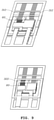
- FIGS. 7 to 11 are process perspective views showing the method of manufacturing the power module according to the exemplary embodiment of the present disclosure step by step.
- the method of manufacturing the power module may be started with preparing the substrate 10 having an upper lead frame 310 , a lower lead frame 320 , the first power semiconductor device 21 , the second power semiconductor device 22 , and the dielectric layer.
- solder S interposed between parts required an electrical connection may also be provided between the substrate 10 and the power semiconductor devices 21 and 22 , between the substrate 10 and the lead frames 310 and 320 , or between the lead frames 310 and 320 .
- the insulating layer 40 to be interposed between the first power lead provided in the upper lead frame 310 and the second power lead provided in the lower lead frame 320 may also be provided.
- the upper lead frame 310 corresponds to a frame in which the first lead part 31 shown in FIGS. 1 to 3 is disposed in a predetermined structure of arrangement and fixed as the frame.
- the lower lead frame 320 corresponds to a frame in which the second lead part 32 shown in FIGS. 1 to 3 is disposed in a predetermined structure of arrangement and fixed as the frame.
- the upper lead frame 310 , the first power semiconductor device 21 , the substrate 10 , the second power semiconductor device 22 , and the lower lead frame 320 are sequentially laminated and soldered to be bonded, thereby making an electrical connection between each of the elements.
- the insulating layer 40 may be disposed between the first power lead and the second power lead so that an upper surface thereof may be contacted with the first power lead and a lower surface thereof may be contacted with the second power lead.
- FIG. 8 schematically shows a structure of arrangement of the insulating layer 40 , but a detailed structure thereof may be easily understood by referring to the structure of arrangement of the insulating layer 40 shown in FIGS. 1 to 3 .
- the first and second power semiconductor devices 21 and 22 may be electrically connected to each other by soldering in the interconnection areas denoted by A of FIGS. 1 to 3 .
- a bonding between the first signal connection lead 312 of the upper lead frame 310 and the signal terminals of the first power semiconductor device is performed by using the bonding wire 60 .
- wire bonding between the second signal connection lead 322 of the lower lead frame 320 and the signal terminals of the second power semiconductor device 22 may be performed.
- the mold part 50 may be formed to cover a laminated structure formed through the soldering of FIG. 8 and the wire bonding part formed through the wire bonding of FIG. 9 .
- molding techniques known in the art such as a transfer molding technique, may be applied.
- the mold part 50 may be formed to expose a part of the upper surface of the upper lead frame and a part of the lower surface of the lower lead frame to the outside of the mold part 50 .
- the power module may be completed by separating and removing the predetermined regions of the upper lead frame 310 and the lower lead frame 320 . Separating and removing the predetermined regions may be performed by removing the frame parts of the upper lead frame 310 and the lower lead frame 320 which are not necessary in the power module structure, and is a step of completing the final shape of the first lead part 31 and the second lead part 32 as shown in FIGS. 1 to 3 .
- Removing a part of the upper lead frame 310 and the lower lead frame 320 from unnecessary parts not required by the power module may be additionally performed as required before forming the mold part.
- the parasitic inductance may be reduced by the dielectric layer disposed at the position between the metal layers when the current flows through the metal layers of the substrate.
- the two power leads face each other by interposing the insulating layer between the two power leads supplying direct current power to the power module, there may be expected an effect in that the parasitic inductance is reduced by the insulating layer.
- the power semiconductor devices are disposed on the upper and lower sides of the substrate, sufficient space may be secured on the upper and lower sides of the power semiconductor device. Therefore, compared with the conventional power module that disposes the power semiconductor devices between both the substrates, the occurrence of interference between the bonding wires and the substrates may be eliminated, and the spacer for securing a distance between the two substrates may be removed.
- the second soldering is required after performing a process of the first soldering and wire bonding, and thus a problem of reducing reliability due to remelting of the solder occurs.
- the number times soldering is performed may be reduced to one time, thereby eliminating the reduced reliability due to remelting, and reducing the process cost.
Landscapes
- Engineering & Computer Science (AREA)
- Ceramic Engineering (AREA)
- Inverter Devices (AREA)
- Chemical & Material Sciences (AREA)
- Physics & Mathematics (AREA)
- Geometry (AREA)
- Structures For Mounting Electric Components On Printed Circuit Boards (AREA)
- Cooling Or The Like Of Semiconductors Or Solid State Devices (AREA)
Abstract
Description
Claims (9)
Applications Claiming Priority (2)
| Application Number | Priority Date | Filing Date | Title |
|---|---|---|---|
| KR1020190167718A KR102731567B1 (en) | 2019-12-16 | 2019-12-16 | Power module and method for manufacturing the same |
| KR10-2019-0167718 | 2019-12-16 |
Publications (2)
| Publication Number | Publication Date |
|---|---|
| US20210183795A1 US20210183795A1 (en) | 2021-06-17 |
| US11227845B2 true US11227845B2 (en) | 2022-01-18 |
Family
ID=76317090
Family Applications (1)
| Application Number | Title | Priority Date | Filing Date |
|---|---|---|---|
| US16/991,293 Active US11227845B2 (en) | 2019-12-16 | 2020-08-12 | Power module and method of manufacturing same |
Country Status (3)
| Country | Link |
|---|---|
| US (1) | US11227845B2 (en) |
| KR (1) | KR102731567B1 (en) |
| CN (1) | CN112992845B (en) |
Families Citing this family (7)
| Publication number | Priority date | Publication date | Assignee | Title |
|---|---|---|---|---|
| CN113257888A (en) * | 2021-03-31 | 2021-08-13 | 华为技术有限公司 | Power semiconductor device, packaging structure and electronic equipment |
| DE102021117822A1 (en) | 2021-07-09 | 2023-01-12 | Danfoss Silicon Power Gmbh | lead frame |
| KR20230172344A (en) * | 2022-06-15 | 2023-12-22 | 현대자동차주식회사 | Power module and motor driving system using the same |
| KR102873894B1 (en) * | 2022-12-30 | 2025-10-17 | 하나 마이크로일렉트로닉스 (자싱) 씨오., 엘티디. | Semiconductor device |
| KR102843819B1 (en) * | 2023-09-14 | 2025-08-07 | (주)라온반도체 | Power module including interconnection structure using printed circuit board |
| KR102846335B1 (en) * | 2023-11-20 | 2025-08-14 | 주식회사 세미파워렉스 | Transfer molded power semiconductor module with assembled signal terminal |
| KR102940062B1 (en) * | 2024-11-13 | 2026-03-17 | 주식회사 세미파워렉스 | Power semiconductor modules with improved electrical and thermal stability |
Citations (4)
| Publication number | Priority date | Publication date | Assignee | Title |
|---|---|---|---|---|
| US20040124539A1 (en) * | 2002-12-31 | 2004-07-01 | Advanced Semiconductor Engineering, Inc. | Multi-chip stack flip-chip package |
| US20090174044A1 (en) * | 2007-12-13 | 2009-07-09 | Eom Joo-Yang | Multi-chip package |
| US20120014059A1 (en) * | 2010-07-15 | 2012-01-19 | Jian-Hong Zeng | Power module |
| US9293680B2 (en) | 2011-06-06 | 2016-03-22 | Gentherm Incorporated | Cartridge-based thermoelectric systems |
Family Cites Families (5)
| Publication number | Priority date | Publication date | Assignee | Title |
|---|---|---|---|---|
| KR101388857B1 (en) * | 2012-06-29 | 2014-04-23 | 삼성전기주식회사 | Semiconductor package and method of manufacturing the semiconductor package |
| JP5704190B2 (en) * | 2013-06-13 | 2015-04-22 | 富士電機株式会社 | Semiconductor power module |
| US10002821B1 (en) * | 2017-09-29 | 2018-06-19 | Infineon Technologies Ag | Semiconductor chip package comprising semiconductor chip and leadframe disposed between two substrates |
| KR102008278B1 (en) * | 2017-12-07 | 2019-08-07 | 현대오트론 주식회사 | Power chip integrated module, its manufacturing method and power module package of double-faced cooling |
| KR102552077B1 (en) * | 2018-04-23 | 2023-07-06 | 현대자동차주식회사 | Power module with stacked and fabricating method thereof |
-
2019
- 2019-12-16 KR KR1020190167718A patent/KR102731567B1/en active Active
-
2020
- 2020-08-12 US US16/991,293 patent/US11227845B2/en active Active
- 2020-09-09 CN CN202010943528.8A patent/CN112992845B/en active Active
Patent Citations (4)
| Publication number | Priority date | Publication date | Assignee | Title |
|---|---|---|---|---|
| US20040124539A1 (en) * | 2002-12-31 | 2004-07-01 | Advanced Semiconductor Engineering, Inc. | Multi-chip stack flip-chip package |
| US20090174044A1 (en) * | 2007-12-13 | 2009-07-09 | Eom Joo-Yang | Multi-chip package |
| US20120014059A1 (en) * | 2010-07-15 | 2012-01-19 | Jian-Hong Zeng | Power module |
| US9293680B2 (en) | 2011-06-06 | 2016-03-22 | Gentherm Incorporated | Cartridge-based thermoelectric systems |
Also Published As
| Publication number | Publication date |
|---|---|
| KR102731567B1 (en) | 2024-11-15 |
| CN112992845A (en) | 2021-06-18 |
| US20210183795A1 (en) | 2021-06-17 |
| KR20210076469A (en) | 2021-06-24 |
| CN112992845B (en) | 2025-07-22 |
Similar Documents
| Publication | Publication Date | Title |
|---|---|---|
| US11227845B2 (en) | Power module and method of manufacturing same | |
| US9899283B2 (en) | Power module with low stray inductance | |
| JP7650635B2 (en) | Half-bridge modules in power electronics traction inverters for electric or hybrid vehicles | |
| US20230171909A1 (en) | Semiconductor device with stacked terminals | |
| US11018109B2 (en) | Power semiconductor module with low gate path inductance | |
| EP3660899B1 (en) | Semiconductor module | |
| US9780684B2 (en) | Power converter | |
| US10027094B2 (en) | Power module, power converter and drive arrangement with a power module | |
| KR20190067566A (en) | Power chip integrated module, its manufacturing method and power module package of double-faced cooling | |
| US11721613B2 (en) | Power module | |
| CN112582356B (en) | Semiconductor Devices | |
| US20250079407A1 (en) | Power electronics module and assembly method | |
| US10304770B2 (en) | Semiconductor device with stacked terminals | |
| US20240379574A1 (en) | Semiconductor device | |
| US12564113B2 (en) | Power electronics module | |
| US11887905B2 (en) | Semiconductor device | |
| JP7641135B2 (en) | Electronic Components and Semiconductor Devices | |
| CN117136434A (en) | Semiconductor device | |
| CN116349011A (en) | Electrical system with electric power module and DC link capacitor and method for manufacturing such an electrical system | |
| JP7841094B2 (en) | Power converter, method for manufacturing a power converter | |
| WO2021014875A1 (en) | Semiconductor device | |
| US20240413119A1 (en) | Contact assembly for power semiconductor chips and power electronics module | |
| JP2025129934A (en) | Semiconductor Module | |
| CN116941035A (en) | Power semiconductor device and power conversion device |
Legal Events
| Date | Code | Title | Description |
|---|---|---|---|
| AS | Assignment |
Owner name: KIA MOTORS CORPORATION, KOREA, REPUBLIC OF Free format text: ASSIGNMENT OF ASSIGNORS INTEREST;ASSIGNORS:LEE, HYUN KOO;PARK, SUNG WON;PARK, JUN HEE;AND OTHERS;REEL/FRAME:053471/0103 Effective date: 20200708 Owner name: HYUNDAI MOTOR COMPANY, KOREA, REPUBLIC OF Free format text: ASSIGNMENT OF ASSIGNORS INTEREST;ASSIGNORS:LEE, HYUN KOO;PARK, SUNG WON;PARK, JUN HEE;AND OTHERS;REEL/FRAME:053471/0103 Effective date: 20200708 |
|
| FEPP | Fee payment procedure |
Free format text: ENTITY STATUS SET TO UNDISCOUNTED (ORIGINAL EVENT CODE: BIG.); ENTITY STATUS OF PATENT OWNER: LARGE ENTITY |
|
| STPP | Information on status: patent application and granting procedure in general |
Free format text: NON FINAL ACTION MAILED |
|
| STPP | Information on status: patent application and granting procedure in general |
Free format text: RESPONSE TO NON-FINAL OFFICE ACTION ENTERED AND FORWARDED TO EXAMINER |
|
| STPP | Information on status: patent application and granting procedure in general |
Free format text: NOTICE OF ALLOWANCE MAILED -- APPLICATION RECEIVED IN OFFICE OF PUBLICATIONS |
|
| STPP | Information on status: patent application and granting procedure in general |
Free format text: PUBLICATIONS -- ISSUE FEE PAYMENT VERIFIED |
|
| STCF | Information on status: patent grant |
Free format text: PATENTED CASE |
|
| MAFP | Maintenance fee payment |
Free format text: PAYMENT OF MAINTENANCE FEE, 4TH YEAR, LARGE ENTITY (ORIGINAL EVENT CODE: M1551); ENTITY STATUS OF PATENT OWNER: LARGE ENTITY Year of fee payment: 4 |