US11227792B2 - Interconnect structures including self aligned vias - Google Patents
Interconnect structures including self aligned vias Download PDFInfo
- Publication number
- US11227792B2 US11227792B2 US16/576,712 US201916576712A US11227792B2 US 11227792 B2 US11227792 B2 US 11227792B2 US 201916576712 A US201916576712 A US 201916576712A US 11227792 B2 US11227792 B2 US 11227792B2
- Authority
- US
- United States
- Prior art keywords
- cap layer
- interlayer dielectric
- self
- interconnect structure
- metal line
- Prior art date
- Legal status (The legal status is an assumption and is not a legal conclusion. Google has not performed a legal analysis and makes no representation as to the accuracy of the status listed.)
- Expired - Fee Related, expires
Links
Images


Classifications
-
- H—ELECTRICITY
- H10—SEMICONDUCTOR DEVICES; ELECTRIC SOLID-STATE DEVICES NOT OTHERWISE PROVIDED FOR
- H10W—GENERIC PACKAGES, INTERCONNECTIONS, CONNECTORS OR OTHER CONSTRUCTIONAL DETAILS OF DEVICES COVERED BY CLASS H10
- H10W20/00—Interconnections in chips, wafers or substrates
- H10W20/01—Manufacture or treatment
- H10W20/071—Manufacture or treatment of dielectric parts thereof
- H10W20/081—Manufacture or treatment of dielectric parts thereof by forming openings in the dielectric parts
-
- H01L21/76802—
-
- H—ELECTRICITY
- H10—SEMICONDUCTOR DEVICES; ELECTRIC SOLID-STATE DEVICES NOT OTHERWISE PROVIDED FOR
- H10W—GENERIC PACKAGES, INTERCONNECTIONS, CONNECTORS OR OTHER CONSTRUCTIONAL DETAILS OF DEVICES COVERED BY CLASS H10
- H10W20/00—Interconnections in chips, wafers or substrates
- H10W20/01—Manufacture or treatment
- H10W20/031—Manufacture or treatment of conductive parts of the interconnections
- H10W20/069—Manufacture or treatment of conductive parts of the interconnections by forming self-aligned vias or self-aligned contact plugs
-
- H01L21/76877—
-
- H01L23/5226—
-
- H01L23/528—
-
- H—ELECTRICITY
- H10—SEMICONDUCTOR DEVICES; ELECTRIC SOLID-STATE DEVICES NOT OTHERWISE PROVIDED FOR
- H10W—GENERIC PACKAGES, INTERCONNECTIONS, CONNECTORS OR OTHER CONSTRUCTIONAL DETAILS OF DEVICES COVERED BY CLASS H10
- H10W20/00—Interconnections in chips, wafers or substrates
- H10W20/01—Manufacture or treatment
- H10W20/031—Manufacture or treatment of conductive parts of the interconnections
- H10W20/056—Manufacture or treatment of conductive parts of the interconnections by filling conductive material into holes, grooves or trenches
-
- H—ELECTRICITY
- H10—SEMICONDUCTOR DEVICES; ELECTRIC SOLID-STATE DEVICES NOT OTHERWISE PROVIDED FOR
- H10W—GENERIC PACKAGES, INTERCONNECTIONS, CONNECTORS OR OTHER CONSTRUCTIONAL DETAILS OF DEVICES COVERED BY CLASS H10
- H10W20/00—Interconnections in chips, wafers or substrates
- H10W20/01—Manufacture or treatment
- H10W20/031—Manufacture or treatment of conductive parts of the interconnections
- H10W20/069—Manufacture or treatment of conductive parts of the interconnections by forming self-aligned vias or self-aligned contact plugs
- H10W20/0693—Manufacture or treatment of conductive parts of the interconnections by forming self-aligned vias or self-aligned contact plugs by forming self-aligned vias
-
- H—ELECTRICITY
- H10—SEMICONDUCTOR DEVICES; ELECTRIC SOLID-STATE DEVICES NOT OTHERWISE PROVIDED FOR
- H10W—GENERIC PACKAGES, INTERCONNECTIONS, CONNECTORS OR OTHER CONSTRUCTIONAL DETAILS OF DEVICES COVERED BY CLASS H10
- H10W20/00—Interconnections in chips, wafers or substrates
- H10W20/01—Manufacture or treatment
- H10W20/071—Manufacture or treatment of dielectric parts thereof
- H10W20/074—Manufacture or treatment of dielectric parts thereof of dielectric parts comprising thin functional dielectric layers, e.g. dielectric etch-stop, barrier, capping or liner layers
-
- H—ELECTRICITY
- H10—SEMICONDUCTOR DEVICES; ELECTRIC SOLID-STATE DEVICES NOT OTHERWISE PROVIDED FOR
- H10W—GENERIC PACKAGES, INTERCONNECTIONS, CONNECTORS OR OTHER CONSTRUCTIONAL DETAILS OF DEVICES COVERED BY CLASS H10
- H10W20/00—Interconnections in chips, wafers or substrates
- H10W20/40—Interconnections external to wafers or substrates, e.g. back-end-of-line [BEOL] metallisations or vias connecting to gate electrodes
- H10W20/41—Interconnections external to wafers or substrates, e.g. back-end-of-line [BEOL] metallisations or vias connecting to gate electrodes characterised by their conductive parts
- H10W20/42—Vias, e.g. via plugs
-
- H—ELECTRICITY
- H10—SEMICONDUCTOR DEVICES; ELECTRIC SOLID-STATE DEVICES NOT OTHERWISE PROVIDED FOR
- H10W—GENERIC PACKAGES, INTERCONNECTIONS, CONNECTORS OR OTHER CONSTRUCTIONAL DETAILS OF DEVICES COVERED BY CLASS H10
- H10W20/00—Interconnections in chips, wafers or substrates
- H10W20/40—Interconnections external to wafers or substrates, e.g. back-end-of-line [BEOL] metallisations or vias connecting to gate electrodes
- H10W20/41—Interconnections external to wafers or substrates, e.g. back-end-of-line [BEOL] metallisations or vias connecting to gate electrodes characterised by their conductive parts
- H10W20/43—Layouts of interconnections
-
- H—ELECTRICITY
- H10—SEMICONDUCTOR DEVICES; ELECTRIC SOLID-STATE DEVICES NOT OTHERWISE PROVIDED FOR
- H10W—GENERIC PACKAGES, INTERCONNECTIONS, CONNECTORS OR OTHER CONSTRUCTIONAL DETAILS OF DEVICES COVERED BY CLASS H10
- H10W20/00—Interconnections in chips, wafers or substrates
- H10W20/01—Manufacture or treatment
- H10W20/031—Manufacture or treatment of conductive parts of the interconnections
- H10W20/032—Manufacture or treatment of conductive parts of the interconnections of conductive barrier, adhesion or liner layers
- H10W20/033—Manufacture or treatment of conductive parts of the interconnections of conductive barrier, adhesion or liner layers in openings in dielectrics
- H10W20/037—Manufacture or treatment of conductive parts of the interconnections of conductive barrier, adhesion or liner layers in openings in dielectrics the barrier, adhesion or liner layers being on top of a main fill metal
-
- H—ELECTRICITY
- H10—SEMICONDUCTOR DEVICES; ELECTRIC SOLID-STATE DEVICES NOT OTHERWISE PROVIDED FOR
- H10W—GENERIC PACKAGES, INTERCONNECTIONS, CONNECTORS OR OTHER CONSTRUCTIONAL DETAILS OF DEVICES COVERED BY CLASS H10
- H10W20/00—Interconnections in chips, wafers or substrates
- H10W20/01—Manufacture or treatment
- H10W20/071—Manufacture or treatment of dielectric parts thereof
- H10W20/074—Manufacture or treatment of dielectric parts thereof of dielectric parts comprising thin functional dielectric layers, e.g. dielectric etch-stop, barrier, capping or liner layers
- H10W20/075—Manufacture or treatment of dielectric parts thereof of dielectric parts comprising thin functional dielectric layers, e.g. dielectric etch-stop, barrier, capping or liner layers of multilayered thin functional dielectric layers
Definitions
- the present invention generally relates to semiconductor devices, interconnect structures, and fabrication methods. More particularly, the present invention relates to self-aligned via interconnect structures and methods for forming the self-aligned via structures to an underlying interconnect.
- An integrated circuit generally includes a semiconductor substrate in which a number of device regions are formed by diffusion or ion implantation of suitable dopants.
- This substrate usually includes various configurations of passivating layers and insulating layers required to form different device regions. Openings through these layers (called vias or contact holes) allow electrical contact to be made selectively to the underlying device regions.
- a conducting material such as copper is used to fill these holes, which then make contact to the appropriate region of the semiconductor device.
- Vias can be formed using a lithographic process.
- a photoresist layer is spin coated over a dielectric layer and subsequently exposed to actinic radiation through a patterned mask, which is developed in order to form an opening in the photoresist layer.
- An opening for the via can be etched in the dielectric layer by using the opening in the photoresist layer as an etch mask. This opening is referred to as a via opening.
- the present invention is generally directed to a semiconductor device, interconnect structures, and methods for forming a semiconductor device including the interconnect structure.
- a method is provided for forming a self-aligned via in a second interconnect structure overlying a first interconnect structure, wherein the first interconnect structure includes a metal line formed in a first interlayer dielectric.
- the method for forming a self-aligned via in a second interconnect structure includes selectively depositing a first cap layer on only exposed surfaces of the metal line formed in the first interlayer dielectric.
- a second cap layer is blanket deposited onto the first interconnect structure.
- the second cap layer is planarized to the metal line, wherein the first cap layer is coplanar to the second cap layer.
- the first cap layer is selectively removed to form a recess exposing the metal line.
- a second interlayer dielectric is deposited and patterned to form a self-aligned via opening to at least a portion of the metal line. A misalignment of the self-aligned via opening results in the at least one self-aligned via opening landing on both the metal line of the first interconnect structure and the second cap layer.
- the semiconductor device includes an interconnect structure for an integrated circuit. More specifically, the semiconductor device can include a first interconnect structure disposed above a substrate.
- the first interconnect structure includes a metal line formed in a first interlayer dielectric.
- a second interconnect structure overlies the first interconnect structure and includes a second cap layer on the first interlayer dielectric, a second interlayer dielectric thereon, and at least one self-aligned via in the second interlayer dielectric conductively coupled to at least a portion of the metal line of the first interconnect structure.
- a misalignment of the at least one self-aligned via results in the at least one self-aligned via landing on both the metal line of the first interconnect structure and the second cap layer, wherein the second cap layer is an insulating material.
- An interconnect structure for an integrated circuit in accordance with one or more embodiments of the invention includes a first interconnect structure disposed above a substrate, the first interconnect structure including a metal line formed in a first interlayer dielectric.
- a second interconnect structure is disposed above the first interconnect structure.
- the second interconnect structure includes a third cap layer selectively provided on only the metal line of the first interconnect structure, a second cap layer on the first interlayer dielectric and the third cap layer, wherein the third cap layer includes an insulating material or a metal material, and wherein the second cap layer is an insulating material, a second interlayer dielectric thereon, and at least one self-aligned via conductively coupled to at least a portion of the metal line of the first interconnect structure.
- a misalignment of the at least one self-aligned via results in the at least one self-aligned via conductively coupled to the metal line of the first interconnect structure and on the second cap layer.
- FIG. 1 illustrates a cross-sectional view of an exemplary semiconductor device including a first interconnect structure including in accordance with one or more embodiments of the present invention
- FIG. 2 illustrates a cross-sectional view of the exemplary semiconductor device of FIG. 1 after selective deposition of a first cap layer onto the wiring structure of the first interconnect structure and deposition of a second cap layer on the substrate in accordance with one or more embodiments of the present invention
- FIG. 3 pictorially illustrates a scanning electron micrograph cross section of the first interconnect structure of FIG. 2 in accordance with one or more embodiments of the present invention
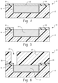
- FIG. 4 depicts a cross-sectional view illustrating the exemplary semiconductor device of FIG. 2 after planarization such that the first and second cap layers are coplanar to one another in accordance with one or more embodiments of the present invention
- FIG. 5 depicts a cross-sectional view illustrating the exemplary semiconductor device of FIG. 4 after selective removal of the first cap layer from the wiring structure of the first interconnect structure so as to form a recess relative to the second cap layer in accordance with one or more embodiments of the present invention
- FIG. 6 depicts a schematic cross-sectional view illustrating the exemplary semiconductor device of FIG. 5 after deposition and patterning a second interlayer dielectric to form a self-aligned via at least partially landing on the wiring structure in accordance with one or more embodiments of the present invention
- FIG. 7 depicts a schematic cross-sectional view of the exemplary semiconductor device of FIG. 5 after deposition and patterning a second interlayer dielectric to form a self-aligned via at least partially landing on the wiring structure in accordance with one or more embodiments of the present invention.
- FIG. 8 illustrates a cross sectional view of the exemplary semiconductor device of FIG. 5 after deposition and patterning a second interlayer dielectric to form a self-aligned via at least partially landing on the wiring structure in accordance with one or more embodiments of the present invention.
- Integrated circuit processing can be generally divided into front end of the line (FEOL), middle of the line (MOL) and back end of the line (BEOL) metallization processes.
- the FEOL and MOL processing will generally form many layers of logical and functional devices.
- the typical FEOL processes include wafer preparation, isolation, well formation, gate patterning, spacer, extension and source/drain implantation, silicide formation, and dual stress liner formation.
- the MOL is mainly gate contact formation. Layers of interconnections are formed above these logical and functional layers during the BEOL metallization processing to complete the integrated circuit structure.
- BEOL metallization processing generally involves the formation of insulators and conductive wiring.
- the present invention generally relates to BEOL structures and processes for forming a self-aligned via to an underlying metal interconnect.
- SAV self-aligned via
- invention or “present invention” are non-limiting terms and not intended to refer to any single aspect of the particular invention but encompass all possible aspects as described in the specification and the claims.
- spatially relative terms e.g., “beneath,” “below,” “lower,” “above,” “upper,” and the like, can be used herein for ease of description to describe one element or feature's relationship to another element(s) or feature(s) as illustrated in the figures. It will be understood that the spatially relative terms are intended to encompass different orientations of the device in use or operation in addition to the orientation depicted in the figures. For example, if the device in the figures is turned over, elements described as “below” or “beneath” other elements or features would then be oriented “above” the other elements or features. Thus, the term “below” can encompass both an orientation of above and below. The device can be otherwise oriented (rotated 90 degrees or at other orientations) and the spatially relative descriptors used herein interpreted accordingly.
- CMOS complementary metal-oxide semiconductor
- FinFET fin field-effect transistor
- MOSFET metal-oxide-semiconductor field-effect transistor
- other semiconductor fabrication techniques and devices may or may not be explicitly shown in a given drawing. This does not imply that the layers and/or regions not explicitly shown are omitted from the actual devices.
- certain elements could be left out of particular views for the sake of clarity and/or simplicity when explanations are not necessarily focused on the omitted elements.
- the same or similar reference numbers used throughout the drawings are used to denote the same or similar features, elements, or structures, and thus, a detailed explanation of the same or similar features, elements, or structures will not be repeated for each of the drawings.
- the semiconductor devices and methods for forming same in accordance with embodiments of the present invention can be employed in applications, hardware, and/or electronic systems.
- Suitable hardware and systems for implementing embodiments of the invention can include, but are not limited to, personal computers, communication networks, electronic commerce systems, portable communications devices (e.g., cell and smart phones), solid-state media storage devices, functional circuitry, etc.
- Systems and hardware incorporating the semiconductor devices are contemplated embodiments of the invention. Given the teachings of embodiments of the invention provided herein, one of ordinary skill in the art will be able to contemplate other implementations and applications of embodiments of the invention.
- the embodiments of the present invention can be used in connection with semiconductor devices that could require, for example, CMOSs, MOSFETs, and/or FinFETs.
- the semiconductor devices can include, but are not limited to CMOS, MOSFET, and FinFET devices, and/or semiconductor devices that use CMOS, MOSFET, and/or FinFET technology.
- compositions comprising, “comprising,” “includes,” “including,” “has,” “having,” “contains” or “containing,” or any other variation thereof, are intended to cover a non-exclusive inclusion.
- a composition, a mixture, process, method, article, or apparatus that comprises a list of elements is not necessarily limited to only those elements but can include other elements not expressly listed or inherent to such composition, mixture, process, method, article, or apparatus.
- the terms “about,” “substantially,” and equivalents thereof modifying the quantity of an ingredient, component, or reactant of the invention employed, or modifying any other quantity or dimension refers to variation in the numerical quantity that can occur, for example, through typical measuring and liquid handling procedures used for making concentrates or solutions. Furthermore, variation can occur from inadvertent error in measuring procedures, differences in the manufacture, source, or purity of the ingredients employed to make the compositions or carry out the methods, and the like.
- the term “about” means within 10% of the reported numerical value.
- the term “about” means within 5% of the reported numerical value.
- the term “about” means within 10, 9, 8, 7, 6, 5, 4, 3, 2, or 1% of the reported numerical value.
- the term “substrate” can include a semiconductor wafer, such as a type IV semiconductor wafer, e.g., silicon wafer, or a type III-V semiconductor wafer, such as a compound semiconductor, e.g., gallium arsenide semiconductor wafer.
- a semiconductor wafer such as a type IV semiconductor wafer, e.g., silicon wafer, or a type III-V semiconductor wafer, such as a compound semiconductor, e.g., gallium arsenide semiconductor wafer.
- several dielectric layers and semiconductor material layers can be arranged with the substrate to provide microelectronic devices, or smaller devices, which can include semiconductor devices, such as field effect transistors (FETs), fin type field effect transistors (FinFETs), bipolar junction transistors (BJT) and combinations thereof.
- FETs field effect transistors
- FinFETs fin type field effect transistors
- BJT bipolar junction transistors
- the at least one device layer can also include memory devices, such as dynamic random access memory (DRAM), embedded dynamic random access memory (EDRAM), flash memory and combinations thereof.
- the at least one device layer can also include passive devices, such as resistors and capacitors, as well as electrical connections to the devices containing within the at least one device layer.
- FIGS. 1-8 schematically illustrate cross sectional views of various BEOL metallization structures and process flows for forming a self-aligned via in the back end of line metallization structure for an integrated circuit in accordance with one or more aspects of the present invention.
- the structures and methods utilize a top via integration scheme to provide alignment in both the orthogonal and parallel directions of the Mx and Mx+1 features.
- FIG. 1 there is shown a cross sectional view of a portion of a first interconnect structure 10 including an interlayer dielectric 12 and a wiring structure 14 formed within the interlayer dielectric 12 .
- the first interconnect structure 10 can be formed on a substrate (not shown).
- the substrate is not intended to be limited and can represent front end of line (FEOL) components.
- FEOL generally refers to the construction of the components of the IC directly inside the wafer.
- the interlayer dielectric 12 can be any dielectric material including inorganic dielectrics or organic dielectrics.
- the dielectric material can be porous or non-porous.
- suitable dielectrics include, but are not limited to: SiO 2 , silsesquioxanes, carbon doped oxides (i.e., organo silicates) that include atoms of Si, C, O and H, thermosetting polyarylene ethers, or multilayers thereof.
- polyarylene is used to denote aryl moieties or inertly substituted aryl moieties which are linked together by bonds, fused rings, or inert linking groups such as, for example, oxygen, sulfur, sulfone, sulfoxide, carbonyl and the like.
- the dielectric layer can be deposited by PECVD procedures as is generally known in the art.
- the interlayer dielectric 12 can be an ultra-low k (ULK) dielectric.
- the ULK dielectric can have a dielectric constant of up to about 3, meaning a dielectric constant of greater than zero up to about 3, such as a dielectric constant ranging from about 1.5 to about 3.0, and in one or more embodiments of the invention, can have a dielectric constant of less than about 2.5.
- the ULK dielectric typically contains pores having characteristic dimensions ranging from about 0.5 nanometers to about 10 nanometers, such as from about 0.5 nanometers to about 2 nanometers.
- Exemplary ULK dielectrics can include porous inorganic materials such as, for example, silicon-containing materials such as compositions of Si, C, O, and H, including (SiCOH), also called C doped oxide (CDO) or organosilicate glass (OSG).
- SiCOH silicon-containing materials
- CDO C doped oxide
- OSG organosilicate glass
- PECVD ULK dielectrics include, but are not limited to, Black Diamond porous SiCOH (BDII, BDIII) from Applied Materials, and ULK or ELK Aurora from ASM.
- spin applied films having the composition Si, C, O, H, such as, methylsilsesquioxanes, siloxanes can also be used.
- the materials known as Orion and other materials from Trikon and the material known as Zircon from Shipley can also be used.
- the ULK dielectric can be a porous low-k organic material such as the commercially available porous organic thermoset from Dow Chemical Co. sold under the tradename porous SiLK, or polyarylene ethers, and the like.
- the wiring structure 14 is formed within the dielectric layer 12 can be formed using lithography, etching, and deposition processes.
- the formation of the wiring structure 14 begins with the deposition and patterning of a photoresist on the interlevel dielectric layer 12 .
- the photoresist is patterned by exposure to energy (light) to form a pattern (openings), which corresponds to the dimensions of the wiring structure 14 .
- a reactive ion etching (RIE) process is performed through the photoresist pattern to form a trench feature.
- the photoresist can then be removed using conventional etchants and/or stripping techniques, e.g., oxygen ashing.
- the photoresist can be composed of a material suitable for use in a lithographic process.
- the photoresist layer is exposed to a light source and subsequently developed.
- the portions of the photoresist layer to be exposed to the light source will be removed upon developing the photoresist layer, e.g., the photoresist layer is composed of a positive photoresist material.
- the photoresist layer is composed of a positive photoresist material such as, but not limited to, a 248 nanometer node resist, a 193 nanometer node resist, a 157 nanometer node resist, an extreme ultra-violet (EUV) resist, or a phenolic resin matrix with a diazonaphthoquinone sensitizer.
- EUV extreme ultra-violet
- the portions of the photoresist to be exposed to the light source will be retained upon developing the photoresist layer, e.g., the photoresist layer is composed of a negative photoresist material.
- a barrier/liner material 16 is formed within the opening.
- the barrier/liner material 16 can be a combination of a barrier metal or metal alloy material and a liner metal or metal alloy material.
- the barrier/liner material 16 is deposited using either plasma vapor deposition (PVD), chemical vapor deposition (CVD) or atomic layer deposition (ALD) processes.
- the barrier material 16 can be tantalum nitride (TaN) or titanium nitride (TiN) with the liner material being Ta or Ti, respectively, or Co.
- An optional seed layer is deposited on the barrier/liner material 16 followed by a deposition of wiring metal to form the wiring structure 14 .
- the optional plating seed layer can be employed to selectively promote subsequent electroplating of a pre-selected conductive metal or metal alloy.
- the optional plating seed layer can include Cu, a Cu alloy, Jr, an Jr alloy, Ru, a Ru alloy (e.g., TaRu alloy) or any other suitable noble metal or noble metal alloy having a low metal-plating overpotential.
- Cu or a Cu alloy plating seed layer is employed, when a Cu metal is to be subsequently formed within the at least one opening.
- other metal materials can also be used for the wiring structure 14 .
- the thickness of the optional seed layer can vary depending on the material of the optional plating seed layer as well as the technique used in forming the same. Typically, the optional plating seed layer has a thickness from 2 nm to 80 nm.
- the optional plating seed layer can be formed by a conventional deposition process including, for example, CVD, PECVD, ALD, and PVD.
- any residual barrier/liner material 16 and metal material for forming the wiring structure 14 can be removed from the upper surface of the interlevel dielectric layer 12 using a chemical mechanical polishing (CMP) process.
- CMP chemical mechanical polishing
- the CMP process can also be used to planarize the wiring structure 14 and the interlevel dielectric layer 12 for subsequent processing such that the uppermost respective surfaces are coplanar to one another as shown.
- a first cap layer 18 is selectively deposited onto the exposed surfaces of the wiring structure 14 .
- the first cap layer 18 is not provided on the exposed surfaces of the interlayer dielectric 12 , thereby forming a raised surface of the first cap layer 18 relative to the uppermost surface of the interlayer dielectric 12 .
- a second cap layer 20 is then blanket deposited onto the structure 10 , wherein the first cap layer 18 is of a different material and has a different etch selectivity than the second cap layer 20 .
- the first cap layer 18 can be an insulative material or a metal material.
- An exemplary insulator is a low k dielectric material such as, for example, NBLok and an exemplary metal layer is cobalt (W, P, B), ruthenium, Ta(N), or the like.
- the thickness of the first cap layer 18 can range from 2 nm to 6 nm.
- the second cap layer 20 can be a dielectric material such as, for example, SixNy, SiC, SiCxNyHz, SiCHN, SiCOH or similar dielectric material, such as, for example, NBLoK, Al 2 O 3 , flowable oxide, tetraethyl orthosilicate, polyimide, or the like provided the dielectric material is different from the insulative materials, if present, selected for the first cap layer 18 .
- a dielectric material such as, for example, SixNy, SiC, SiCxNyHz, SiCHN, SiCOH or similar dielectric material, such as, for example, NBLoK, Al 2 O 3 , flowable oxide, tetraethyl orthosilicate, polyimide, or the like provided the dielectric material is different from the insulative materials, if present, selected for the first cap layer 18 .
- FIG. 3 pictorially illustrates a cross sectional scanning electron micrograph of the first interconnect structure of FIG. 2 including the wiring structure 14 within the interlayer dielectric 12 , wherein the first and second cap layers 18 , 20 , respectively are provided on the first interconnect structure as described above.
- the first cap layer can be a metal cap layer having a thickness of about 25 nanometers.
- the first cap layer 18 can optionally be a metal material.
- the BEOL metallization structure 10 is subjected to a planarization process stopping on the first cap layer 18 such that the uppermost surfaces of the first and second cap layers 18 , 20 , respectively, are coplanar to one another.
- An exemplary planarization process is a chemical mechanical polishing process (CMP).
- the first cap layer is selectively removed.
- Selective removal of the first cap layer relative to the second cap layer can include an etching process.
- the etching process can be a dry etching process or a wet etching process depending on the materials defining the first and second cap layers.
- wet etching generally refers to application of a chemical solution.
- dry etching is used here to denote an etching technique such as reactive-ion-etching (RIE), ion beam etching, plasma etching or laser ablation.
- RIE reactive-ion-etching
- the pattern can be first transferred using a photoresist to a dielectric layer.
- the patterned photoresist is typically, but not necessarily, removed from the structure after the pattern has been transferred into the dielectric film.
- the first cap material can be selectively removed using a wet etching process, for example, that is selective to the material (e.g., metal or insulative material) used to define the first cap layer 18 relative to the material (e.g., insulative material) used to define the second cap layer 20 and underlying metal utilized for the wiring structure 14 .
- a wet etching process for example, that is selective to the material (e.g., metal or insulative material) used to define the first cap layer 18 relative to the material (e.g., insulative material) used to define the second cap layer 20 and underlying metal utilized for the wiring structure 14 .
- a second interlayer dielectric layer 22 is deposited onto the BEOL metallization structure 10 and lithographically patterned to form a self-aligned via opening 24 to the underlying wiring structure 14 .
- the self-aligned via opening can be formed using a directional etching process such as reactive ion etching.
- CF 4 , CHF 3 , C x H y F z /N 2 process gases can be used in the directional etching process.
- the self-aligned via opening 24 partially lands on the wiring structure 14 but is stopped on the second cap layer 20 .
- the second capping layer 20 serves to prevent undesirable diffusion of the underlying wiring structure 14 into dielectric layer 12 , which improves reliability of the interconnect structure.
- the self-aligned via opening is offset relative to the underlying wiring structure 14 and partially lands on the wiring structure 14 .
- the offset pattern refers to misalignment with the openings in the metal hard mask layer that is typically used to form the self-aligned via opening.
- the offset pattern depicted can represent an offset tolerance with the fabrication of commercial wafers. Or, in another case, the offset can be intentionally formed for the sake of optimizing a self-aligned via etch with hard mask selectivity.
- a third cap layer 28 is conformally deposited onto the BEOL metallization structure 10 subsequent to selective removal of the first cap layer 18 shown in FIG. 5 . That is, a relatively thin layer of the third cap layer 28 (relative to the thickness of the first cap layer 18 initially deposited as discussed in relation to FIG. 2 ) is conformally deposited onto the topography defined by the non-planar surfaces of the second cap layer 20 and the wiring structure 14 .
- the third cap layer 28 is an insulating material such as, for example, SiC, SiN, SiC (N,H) or the like.
- the second interlayer dielectric layer 22 is then deposited onto the BEOL metallization structure 10 and lithographically patterned to form a self-aligned via opening 30 to the underlying wiring structure 14 .
- the self-aligned via opening 30 can be formed using a directional etching process such as reactive ion etching as previously described.
- the self-aligned via directional etching process is configured to selectively remove exposed portions of the second dielectric 22 and the insulative third cap layer 28 at the bottom of the via opening 30 , thereby exposing a portion of the wiring structure 14 and a portion of the second cap layer 20 as a result of lateral misalignment to the wiring structure 14 .
- the via opening 24 partially lands on the wiring structure 14 but is stopped on the second cap layer 20 .
- the presence of the second cap layer 20 at the bottom of the via opening 30 prevents degradation of the interconnect connection and enables self-alignment of the via opening 30 landing on at least a portion of the wiring structure 14 , which is subsequently filled with a suitable conductor.
- the presence of the second cap layer 20 prevents undesirable diffusion of the underlying wiring structure 14 or the metal filled self-aligned via into dielectric layer 12 .
- the presence of the third cap layer 28 on the wiring structure 14 prevents diffusion into the interlayer dielectric 22 .
- a metal cap layer 38 such as, for example, ruthenium, cobalt, tungsten, alloys thereof or the like, is selectively deposited onto the wiring structure 14 subsequent to selective removal of the first cap layer 18 as previously described and shown in FIG. 5 .
- the second interlayer dielectric layer 22 is then deposited onto the BEOL metallization structure 10 and lithographically patterned to form a via opening 40 to the underlying wiring structure 14 .
- the via opening 40 can be formed using a directional etching process such as reactive ion etching as previously described.
- the directional etching process is configured to selectively remove exposed portions of the second dielectric 22 and the exposed surface of the metal cap layer 38 at the bottom of the via opening 40 that had been selectively deposited onto the wiring structure, thereby exposing a portion of the wiring structure 14 and a portion of the second cap layer 20 as a result of lateral misalignment to the wiring structure 14 .
- the self-aligned via opening 40 partially lands on the wiring structure 14 but is stopped on the second cap layer 20 .
- the presence of the second cap layer 20 at the bottom of the via opening 40 prevents degradation of the interconnect connection and enables self-alignment of the via opening 30 landing on at least a portion of the wiring structure 14 , which is subsequently filled with a suitable conductor.
- the presence of the second cap layer 20 prevents undesirable diffusion of the underlying wiring structure 14 or the metal filled self-aligned via into dielectric layer 12 .
- the presence of the third cap layer 28 formed of ruthenium, cobalt, tungsten, alloys thereof or the like on the wiring structure 14 prevents diffusion into the interlayer dielectric 22 .
- the capping layers 18 , 20 , 28 , 38 can protect the underlying metal conductive line 14 from oxidation, humidity, and contamination during processing of the next metal levels on the semiconductor wafer 10 . Additionally, capping layer serves to prevent undesirable diffusion of the underlying conductive line 14 into interlayer dielectric 12 , 20 . Still further, the structures and process including the self-aligned vias overcomes some of the challenges in the prior art and improves overlay tolerance by eliminating any issues related to misalignment of the self-aligned vias to the wiring structure. So long as the self-aligned vias partially land on the wiring structure, reliability is not impacted, and any issues related to orthogonal and parallel alignment of the self-aligned vias are minimized.
Landscapes
- Physics & Mathematics (AREA)
- Geometry (AREA)
- Internal Circuitry In Semiconductor Integrated Circuit Devices (AREA)
Abstract
Description
Claims (7)
Priority Applications (2)
| Application Number | Priority Date | Filing Date | Title |
|---|---|---|---|
| US16/576,712 US11227792B2 (en) | 2019-09-19 | 2019-09-19 | Interconnect structures including self aligned vias |
| US17/541,450 US11735468B2 (en) | 2019-09-19 | 2021-12-03 | Interconnect structures including self aligned vias |
Applications Claiming Priority (1)
| Application Number | Priority Date | Filing Date | Title |
|---|---|---|---|
| US16/576,712 US11227792B2 (en) | 2019-09-19 | 2019-09-19 | Interconnect structures including self aligned vias |
Related Child Applications (1)
| Application Number | Title | Priority Date | Filing Date |
|---|---|---|---|
| US17/541,450 Division US11735468B2 (en) | 2019-09-19 | 2021-12-03 | Interconnect structures including self aligned vias |
Publications (2)
| Publication Number | Publication Date |
|---|---|
| US20210090942A1 US20210090942A1 (en) | 2021-03-25 |
| US11227792B2 true US11227792B2 (en) | 2022-01-18 |
Family
ID=74879994
Family Applications (2)
| Application Number | Title | Priority Date | Filing Date |
|---|---|---|---|
| US16/576,712 Expired - Fee Related US11227792B2 (en) | 2019-09-19 | 2019-09-19 | Interconnect structures including self aligned vias |
| US17/541,450 Active 2039-10-24 US11735468B2 (en) | 2019-09-19 | 2021-12-03 | Interconnect structures including self aligned vias |
Family Applications After (1)
| Application Number | Title | Priority Date | Filing Date |
|---|---|---|---|
| US17/541,450 Active 2039-10-24 US11735468B2 (en) | 2019-09-19 | 2021-12-03 | Interconnect structures including self aligned vias |
Country Status (1)
| Country | Link |
|---|---|
| US (2) | US11227792B2 (en) |
Families Citing this family (8)
| Publication number | Priority date | Publication date | Assignee | Title |
|---|---|---|---|---|
| US10770286B2 (en) * | 2017-05-08 | 2020-09-08 | Asm Ip Holdings B.V. | Methods for selectively forming a silicon nitride film on a substrate and related semiconductor device structures |
| US10515896B2 (en) * | 2017-08-31 | 2019-12-24 | Taiwan Semiconductor Manufacturing Co., Ltd. | Interconnect structure for semiconductor device and methods of fabrication thereof |
| US11227792B2 (en) | 2019-09-19 | 2022-01-18 | International Business Machines Corporation | Interconnect structures including self aligned vias |
| US11935784B2 (en) | 2021-06-11 | 2024-03-19 | Sandisk Technologies Llc | Three-dimensional memory device containing self-aligned bit line contacts and methods for forming the same |
| US12525487B2 (en) | 2021-10-25 | 2026-01-13 | SanDisk Technologies, Inc. | High aspect ratio via fill process employing selective metal deposition and structures formed by the same |
| US12456688B2 (en) | 2021-10-25 | 2025-10-28 | SanDisk Technologies, Inc. | High aspect ratio via fill process employing selective metal deposition and structures formed by the same |
| US12087626B2 (en) | 2021-10-25 | 2024-09-10 | Sandisk Technologies Llc | High aspect ratio via fill process employing selective metal deposition and structures formed by the same |
| US12087628B2 (en) | 2021-10-25 | 2024-09-10 | Sandisk Technologies Llc | High aspect ratio via fill process employing selective metal deposition and structures formed by the same |
Citations (23)
| Publication number | Priority date | Publication date | Assignee | Title |
|---|---|---|---|---|
| US5891513A (en) | 1996-01-16 | 1999-04-06 | Cornell Research Foundation | Electroless CU deposition on a barrier layer by CU contact displacement for ULSI applications |
| US6143645A (en) | 1997-02-03 | 2000-11-07 | Texas Instruments Incorporated | Reduced temperature contact/via filling |
| US20020121699A1 (en) | 2001-03-01 | 2002-09-05 | Kuan-Lun Cheng | Dual damascene Cu contact plug using selective tungsten deposition |
| US7086138B2 (en) | 2000-10-06 | 2006-08-08 | Seagate Technology Llc | Method of forming a feature having a high aspect ratio |
| US7514361B2 (en) | 2007-08-20 | 2009-04-07 | International Business Machines Corporation | Selective thin metal cap process |
| US7727888B2 (en) | 2005-08-31 | 2010-06-01 | International Business Machines Corporation | Interconnect structure and method for forming the same |
| US7745282B2 (en) | 2007-02-16 | 2010-06-29 | International Business Machines Corporation | Interconnect structure with bi-layer metal cap |
| US8039966B2 (en) | 2009-09-03 | 2011-10-18 | International Business Machines Corporation | Structures of and methods and tools for forming in-situ metallic/dielectric caps for interconnects |
| US8138604B2 (en) | 2007-06-21 | 2012-03-20 | International Business Machines Corporation | Metal cap with ultra-low k dielectric material for circuit interconnect applications |
| US8299625B2 (en) | 2010-10-07 | 2012-10-30 | International Business Machines Corporation | Borderless interconnect line structure self-aligned to upper and lower level contact vias |
| US8614144B2 (en) | 2011-06-10 | 2013-12-24 | Kabushiki Kaisha Toshiba | Method for fabrication of interconnect structure with improved alignment for semiconductor devices |
| US20140319650A1 (en) * | 2013-04-26 | 2014-10-30 | International Business Machines Corporation | Programmable electrical fuse |
| US20150091181A1 (en) * | 2013-09-30 | 2015-04-02 | International Business Machines Corporation | Self-aligned vias formed using sacrificial metal caps |
| US20160027738A1 (en) * | 2014-07-24 | 2016-01-28 | International Business Machines Corporation | Semiconductor device with reduced via resistance |
| US9324650B2 (en) | 2014-08-15 | 2016-04-26 | International Business Machines Corporation | Interconnect structures with fully aligned vias |
| US20160329278A1 (en) | 2015-05-08 | 2016-11-10 | Globalfoundries Inc. | 2d self-aligned via first process flow |
| US20160379881A1 (en) * | 2015-06-26 | 2016-12-29 | GlobalFoundries, Inc. | Integrated circuits with self aligned contacts and methods of manufacturing the same |
| US20170186743A1 (en) * | 2015-12-28 | 2017-06-29 | Taiwan Semiconductor Manufacturing Co., Ltd. | Semiconductor device and a method for fabricating the same |
| US20170186682A1 (en) * | 2015-12-28 | 2017-06-29 | Globalfoundries Inc. | Self-aligned via forming to conductive line and related wiring structure |
| US9818640B1 (en) | 2016-09-21 | 2017-11-14 | Globalfoundries Inc. | Apparatus and method of forming self-aligned cuts in a non-mandrel line of an array of metal lines |
| US20180138187A1 (en) | 2016-11-15 | 2018-05-17 | Globalfoundries Inc. | Methods of forming semiconductor devices using semi-bidirectional patterning |
| US10199270B2 (en) | 2017-05-25 | 2019-02-05 | Globalfoundries Inc. | Multi-directional self-aligned multiple patterning |
| US20190096819A1 (en) * | 2017-09-22 | 2019-03-28 | United Microelectronics Corp. | Metal interconnect structure and method for fabricating the same |
Family Cites Families (28)
| Publication number | Priority date | Publication date | Assignee | Title |
|---|---|---|---|---|
| JP2003068850A (en) * | 2001-08-29 | 2003-03-07 | Tokyo Electron Ltd | Semiconductor device and method of manufacturing the same |
| US20030134499A1 (en) * | 2002-01-15 | 2003-07-17 | International Business Machines Corporation | Bilayer HDP CVD / PE CVD cap in advanced BEOL interconnect structures and method thereof |
| US6867125B2 (en) * | 2002-09-26 | 2005-03-15 | Intel Corporation | Creating air gap in multi-level metal interconnects using electron beam to remove sacrificial material |
| US7238604B2 (en) * | 2003-04-24 | 2007-07-03 | Intel Corporation | Forming thin hard mask over air gap or porous dielectric |
| US7279411B2 (en) * | 2005-11-15 | 2007-10-09 | International Business Machines Corporation | Process for forming a redundant structure |
| JP2010287831A (en) * | 2009-06-15 | 2010-12-24 | Renesas Electronics Corp | Semiconductor device and manufacturing method thereof |
| FR2969375A1 (en) * | 2010-12-17 | 2012-06-22 | St Microelectronics Crolles 2 | INTERCONNECTION STRUCTURE FOR INTEGRATED CIRCUIT |
| KR101728288B1 (en) * | 2011-12-30 | 2017-04-18 | 인텔 코포레이션 | Self-enclosed asymmetric interconnect structures |
| US9245789B2 (en) * | 2012-10-09 | 2016-01-26 | Nec Corporation | Method for forming wiring |
| US8772938B2 (en) * | 2012-12-04 | 2014-07-08 | Intel Corporation | Semiconductor interconnect structures |
| US9397045B2 (en) * | 2014-10-16 | 2016-07-19 | Taiwan Semiconductor Manufacturing Co., Ltd | Structure and formation method of damascene structure |
| US9437484B2 (en) * | 2014-10-17 | 2016-09-06 | Taiwan Semiconductor Manufacturing Company, Ltd. | Etch stop layer in integrated circuits |
| US9659864B2 (en) * | 2015-10-20 | 2017-05-23 | Taiwan Semiconductor Manufacturing Company, Ltd. | Method and apparatus for forming self-aligned via with selectively deposited etching stop layer |
| US9818690B2 (en) * | 2015-10-30 | 2017-11-14 | Taiwan Semiconductor Manufacturing Company, Ltd. | Self-aligned interconnection structure and method |
| US10211148B2 (en) * | 2015-12-14 | 2019-02-19 | International Business Machines Corporation | Structural enhancement of Cu nanowires |
| US9536832B1 (en) * | 2015-12-30 | 2017-01-03 | International Business Machines Corporation | Junctionless back end of the line via contact |
| US9530691B1 (en) * | 2016-02-19 | 2016-12-27 | Globalfoundries Inc. | Methods, apparatus and system for forming a dielectric field for dual orientation self aligned vias |
| US9935051B2 (en) * | 2016-08-18 | 2018-04-03 | International Business Machines Corporation | Multi-level metallization interconnect structure |
| US10453749B2 (en) * | 2017-02-14 | 2019-10-22 | Tokyo Electron Limited | Method of forming a self-aligned contact using selective SiO2 deposition |
| US10734278B2 (en) * | 2018-06-15 | 2020-08-04 | Tokyo Electron Limited | Method of protecting low-K layers |
| US10867805B2 (en) * | 2018-06-29 | 2020-12-15 | Taiwan Semiconductor Manufacturing Co., Ltd. | Selective removal of an etching stop layer for improving overlay shift tolerance |
| KR102580659B1 (en) * | 2018-10-01 | 2023-09-20 | 삼성전자주식회사 | Semiconductor devices and methods of manufacturing the same |
| US11502001B2 (en) * | 2018-10-31 | 2022-11-15 | Taiwan Semiconductor Manufacturing Company, Ltd. | Semiconductor device with self-aligned vias |
| US10957579B2 (en) * | 2018-11-06 | 2021-03-23 | Samsung Electronics Co., Ltd. | Integrated circuit devices including a via and methods of forming the same |
| US10886462B2 (en) * | 2018-11-19 | 2021-01-05 | International Business Machines Corporation | Encapsulated memory pillars |
| US11152298B2 (en) * | 2019-06-04 | 2021-10-19 | International Business Machines Corporation | Metal via structure |
| US11227792B2 (en) | 2019-09-19 | 2022-01-18 | International Business Machines Corporation | Interconnect structures including self aligned vias |
| US11289375B2 (en) * | 2020-03-23 | 2022-03-29 | International Business Machines Corporation | Fully aligned interconnects with selective area deposition |
-
2019
- 2019-09-19 US US16/576,712 patent/US11227792B2/en not_active Expired - Fee Related
-
2021
- 2021-12-03 US US17/541,450 patent/US11735468B2/en active Active
Patent Citations (23)
| Publication number | Priority date | Publication date | Assignee | Title |
|---|---|---|---|---|
| US5891513A (en) | 1996-01-16 | 1999-04-06 | Cornell Research Foundation | Electroless CU deposition on a barrier layer by CU contact displacement for ULSI applications |
| US6143645A (en) | 1997-02-03 | 2000-11-07 | Texas Instruments Incorporated | Reduced temperature contact/via filling |
| US7086138B2 (en) | 2000-10-06 | 2006-08-08 | Seagate Technology Llc | Method of forming a feature having a high aspect ratio |
| US20020121699A1 (en) | 2001-03-01 | 2002-09-05 | Kuan-Lun Cheng | Dual damascene Cu contact plug using selective tungsten deposition |
| US7727888B2 (en) | 2005-08-31 | 2010-06-01 | International Business Machines Corporation | Interconnect structure and method for forming the same |
| US7745282B2 (en) | 2007-02-16 | 2010-06-29 | International Business Machines Corporation | Interconnect structure with bi-layer metal cap |
| US8138604B2 (en) | 2007-06-21 | 2012-03-20 | International Business Machines Corporation | Metal cap with ultra-low k dielectric material for circuit interconnect applications |
| US7514361B2 (en) | 2007-08-20 | 2009-04-07 | International Business Machines Corporation | Selective thin metal cap process |
| US8039966B2 (en) | 2009-09-03 | 2011-10-18 | International Business Machines Corporation | Structures of and methods and tools for forming in-situ metallic/dielectric caps for interconnects |
| US8299625B2 (en) | 2010-10-07 | 2012-10-30 | International Business Machines Corporation | Borderless interconnect line structure self-aligned to upper and lower level contact vias |
| US8614144B2 (en) | 2011-06-10 | 2013-12-24 | Kabushiki Kaisha Toshiba | Method for fabrication of interconnect structure with improved alignment for semiconductor devices |
| US20140319650A1 (en) * | 2013-04-26 | 2014-10-30 | International Business Machines Corporation | Programmable electrical fuse |
| US20150091181A1 (en) * | 2013-09-30 | 2015-04-02 | International Business Machines Corporation | Self-aligned vias formed using sacrificial metal caps |
| US20160027738A1 (en) * | 2014-07-24 | 2016-01-28 | International Business Machines Corporation | Semiconductor device with reduced via resistance |
| US9324650B2 (en) | 2014-08-15 | 2016-04-26 | International Business Machines Corporation | Interconnect structures with fully aligned vias |
| US20160329278A1 (en) | 2015-05-08 | 2016-11-10 | Globalfoundries Inc. | 2d self-aligned via first process flow |
| US20160379881A1 (en) * | 2015-06-26 | 2016-12-29 | GlobalFoundries, Inc. | Integrated circuits with self aligned contacts and methods of manufacturing the same |
| US20170186743A1 (en) * | 2015-12-28 | 2017-06-29 | Taiwan Semiconductor Manufacturing Co., Ltd. | Semiconductor device and a method for fabricating the same |
| US20170186682A1 (en) * | 2015-12-28 | 2017-06-29 | Globalfoundries Inc. | Self-aligned via forming to conductive line and related wiring structure |
| US9818640B1 (en) | 2016-09-21 | 2017-11-14 | Globalfoundries Inc. | Apparatus and method of forming self-aligned cuts in a non-mandrel line of an array of metal lines |
| US20180138187A1 (en) | 2016-11-15 | 2018-05-17 | Globalfoundries Inc. | Methods of forming semiconductor devices using semi-bidirectional patterning |
| US10199270B2 (en) | 2017-05-25 | 2019-02-05 | Globalfoundries Inc. | Multi-directional self-aligned multiple patterning |
| US20190096819A1 (en) * | 2017-09-22 | 2019-03-28 | United Microelectronics Corp. | Metal interconnect structure and method for fabricating the same |
Also Published As
| Publication number | Publication date |
|---|---|
| US20210090942A1 (en) | 2021-03-25 |
| US11735468B2 (en) | 2023-08-22 |
| US20220093453A1 (en) | 2022-03-24 |
Similar Documents
| Publication | Publication Date | Title |
|---|---|---|
| US11735468B2 (en) | Interconnect structures including self aligned vias | |
| US12444687B2 (en) | Interconnect structure with vias extending through multiple dielectric layers | |
| US10141220B2 (en) | Via patterning using multiple photo multiple etch | |
| US10867921B2 (en) | Semiconductor structure with tapered conductor | |
| US10777735B2 (en) | Contact via structures | |
| US9390967B2 (en) | Method for residue-free block pattern transfer onto metal interconnects for air gap formation | |
| US9576894B2 (en) | Integrated circuits including organic interlayer dielectric layers and methods for fabricating the same | |
| US11239165B2 (en) | Method of forming an interconnect structure with enhanced corner connection | |
| US10727114B2 (en) | Interconnect structure including airgaps and substractively etched metal lines | |
| US10879190B2 (en) | Patterning integration scheme with trench alignment marks | |
| US10734277B2 (en) | Top via back end of the line interconnect integration | |
| CN112951721B (en) | Trench Etch Process for Photoresist Line Roughness Improvement | |
| US11244897B2 (en) | Back end of line metallization | |
| US9406617B1 (en) | Structure and process for W contacts | |
| US11289375B2 (en) | Fully aligned interconnects with selective area deposition | |
| US20230377956A1 (en) | Method of forming an interconect structure of a semiconductor device | |
| TWI898595B (en) | Semiconductor structure and method of forming the same | |
| US11031542B2 (en) | Contact via with pillar of alternating layers | |
| US12400875B2 (en) | Film deposition for patterning process | |
| JP2006049534A (en) | Semiconductor device and manufacturing method thereof |
Legal Events
| Date | Code | Title | Description |
|---|---|---|---|
| FEPP | Fee payment procedure |
Free format text: ENTITY STATUS SET TO UNDISCOUNTED (ORIGINAL EVENT CODE: BIG.); ENTITY STATUS OF PATENT OWNER: LARGE ENTITY |
|
| AS | Assignment |
Owner name: INTERNATIONAL BUSINESS MACHINES CORPORATION, NEW YORK Free format text: ASSIGNMENT OF ASSIGNORS INTEREST;ASSIGNORS:YANG, CHIH-CHAO;SPOONER, TERRY A.;MOTOYAMA, KOICHI;AND OTHERS;SIGNING DATES FROM 20190916 TO 20190917;REEL/FRAME:050440/0178 |
|
| STPP | Information on status: patent application and granting procedure in general |
Free format text: RESPONSE TO NON-FINAL OFFICE ACTION ENTERED AND FORWARDED TO EXAMINER |
|
| STPP | Information on status: patent application and granting procedure in general |
Free format text: FINAL REJECTION MAILED |
|
| STPP | Information on status: patent application and granting procedure in general |
Free format text: DOCKETED NEW CASE - READY FOR EXAMINATION |
|
| STPP | Information on status: patent application and granting procedure in general |
Free format text: NOTICE OF ALLOWANCE MAILED -- APPLICATION RECEIVED IN OFFICE OF PUBLICATIONS |
|
| STPP | Information on status: patent application and granting procedure in general |
Free format text: PUBLICATIONS -- ISSUE FEE PAYMENT RECEIVED |
|
| STPP | Information on status: patent application and granting procedure in general |
Free format text: PUBLICATIONS -- ISSUE FEE PAYMENT VERIFIED |
|
| STCF | Information on status: patent grant |
Free format text: PATENTED CASE |
|
| FEPP | Fee payment procedure |
Free format text: MAINTENANCE FEE REMINDER MAILED (ORIGINAL EVENT CODE: REM.); ENTITY STATUS OF PATENT OWNER: LARGE ENTITY |
|
| LAPS | Lapse for failure to pay maintenance fees |
Free format text: PATENT EXPIRED FOR FAILURE TO PAY MAINTENANCE FEES (ORIGINAL EVENT CODE: EXP.); ENTITY STATUS OF PATENT OWNER: LARGE ENTITY |
|
| STCH | Information on status: patent discontinuation |
Free format text: PATENT EXPIRED DUE TO NONPAYMENT OF MAINTENANCE FEES UNDER 37 CFR 1.362 |
|
| FP | Lapsed due to failure to pay maintenance fee |
Effective date: 20260118 |