US11227652B2 - Memory device and method of operating the same - Google Patents
Memory device and method of operating the same Download PDFInfo
- Publication number
- US11227652B2 US11227652B2 US16/997,432 US202016997432A US11227652B2 US 11227652 B2 US11227652 B2 US 11227652B2 US 202016997432 A US202016997432 A US 202016997432A US 11227652 B2 US11227652 B2 US 11227652B2
- Authority
- US
- United States
- Prior art keywords
- data
- cam
- extra
- register
- memory device
- Prior art date
- Legal status (The legal status is an assumption and is not a legal conclusion. Google has not performed a legal analysis and makes no representation as to the accuracy of the status listed.)
- Active
Links
Images


Classifications
-
- G—PHYSICS
- G11—INFORMATION STORAGE
- G11C—STATIC STORES
- G11C15/00—Digital stores in which information comprising one or more characteristic parts is written into the store and in which information is read-out by searching for one or more of these characteristic parts, i.e. associative or content-addressed stores
- G11C15/04—Digital stores in which information comprising one or more characteristic parts is written into the store and in which information is read-out by searching for one or more of these characteristic parts, i.e. associative or content-addressed stores using semiconductor elements
-
- G—PHYSICS
- G06—COMPUTING OR CALCULATING; COUNTING
- G06F—ELECTRIC DIGITAL DATA PROCESSING
- G06F3/00—Input arrangements for transferring data to be processed into a form capable of being handled by the computer; Output arrangements for transferring data from processing unit to output unit, e.g. interface arrangements
- G06F3/06—Digital input from, or digital output to, record carriers, e.g. RAID, emulated record carriers or networked record carriers
- G06F3/0601—Interfaces specially adapted for storage systems
- G06F3/0628—Interfaces specially adapted for storage systems making use of a particular technique
- G06F3/0629—Configuration or reconfiguration of storage systems
-
- G—PHYSICS
- G11—INFORMATION STORAGE
- G11C—STATIC STORES
- G11C11/00—Digital stores characterised by the use of particular electric or magnetic storage elements; Storage elements therefor
- G11C11/21—Digital stores characterised by the use of particular electric or magnetic storage elements; Storage elements therefor using electric elements
- G11C11/34—Digital stores characterised by the use of particular electric or magnetic storage elements; Storage elements therefor using electric elements using semiconductor devices
- G11C11/40—Digital stores characterised by the use of particular electric or magnetic storage elements; Storage elements therefor using electric elements using semiconductor devices using transistors
- G11C11/401—Digital stores characterised by the use of particular electric or magnetic storage elements; Storage elements therefor using electric elements using semiconductor devices using transistors forming cells needing refreshing or charge regeneration, i.e. dynamic cells
- G11C11/4063—Auxiliary circuits, e.g. for addressing, decoding, driving, writing, sensing or timing
- G11C11/407—Auxiliary circuits, e.g. for addressing, decoding, driving, writing, sensing or timing for memory cells of the field-effect type
- G11C11/409—Read-write [R-W] circuits
- G11C11/4093—Input/output [I/O] data interface arrangements, e.g. data buffers
-
- G—PHYSICS
- G06—COMPUTING OR CALCULATING; COUNTING
- G06F—ELECTRIC DIGITAL DATA PROCESSING
- G06F11/00—Error detection; Error correction; Monitoring
- G06F11/07—Responding to the occurrence of a fault, e.g. fault tolerance
- G06F11/08—Error detection or correction by redundancy in data representation, e.g. by using checking codes
- G06F11/10—Adding special bits or symbols to the coded information, e.g. parity check, casting out 9's or 11's
- G06F11/1004—Adding special bits or symbols to the coded information, e.g. parity check, casting out 9's or 11's to protect a block of data words, e.g. CRC or checksum
-
- G—PHYSICS
- G06—COMPUTING OR CALCULATING; COUNTING
- G06F—ELECTRIC DIGITAL DATA PROCESSING
- G06F11/00—Error detection; Error correction; Monitoring
- G06F11/07—Responding to the occurrence of a fault, e.g. fault tolerance
- G06F11/08—Error detection or correction by redundancy in data representation, e.g. by using checking codes
- G06F11/10—Adding special bits or symbols to the coded information, e.g. parity check, casting out 9's or 11's
- G06F11/1008—Adding special bits or symbols to the coded information, e.g. parity check, casting out 9's or 11's in individual solid state devices
- G06F11/1064—Adding special bits or symbols to the coded information, e.g. parity check, casting out 9's or 11's in individual solid state devices in cache or content addressable memories
-
- G—PHYSICS
- G06—COMPUTING OR CALCULATING; COUNTING
- G06F—ELECTRIC DIGITAL DATA PROCESSING
- G06F11/00—Error detection; Error correction; Monitoring
- G06F11/07—Responding to the occurrence of a fault, e.g. fault tolerance
- G06F11/08—Error detection or correction by redundancy in data representation, e.g. by using checking codes
- G06F11/10—Adding special bits or symbols to the coded information, e.g. parity check, casting out 9's or 11's
- G06F11/1008—Adding special bits or symbols to the coded information, e.g. parity check, casting out 9's or 11's in individual solid state devices
- G06F11/1068—Adding special bits or symbols to the coded information, e.g. parity check, casting out 9's or 11's in individual solid state devices in sector programmable memories, e.g. flash disk
-
- G—PHYSICS
- G06—COMPUTING OR CALCULATING; COUNTING
- G06F—ELECTRIC DIGITAL DATA PROCESSING
- G06F3/00—Input arrangements for transferring data to be processed into a form capable of being handled by the computer; Output arrangements for transferring data from processing unit to output unit, e.g. interface arrangements
- G06F3/06—Digital input from, or digital output to, record carriers, e.g. RAID, emulated record carriers or networked record carriers
- G06F3/0601—Interfaces specially adapted for storage systems
- G06F3/0602—Interfaces specially adapted for storage systems specifically adapted to achieve a particular effect
- G06F3/0614—Improving the reliability of storage systems
-
- G—PHYSICS
- G06—COMPUTING OR CALCULATING; COUNTING
- G06F—ELECTRIC DIGITAL DATA PROCESSING
- G06F3/00—Input arrangements for transferring data to be processed into a form capable of being handled by the computer; Output arrangements for transferring data from processing unit to output unit, e.g. interface arrangements
- G06F3/06—Digital input from, or digital output to, record carriers, e.g. RAID, emulated record carriers or networked record carriers
- G06F3/0601—Interfaces specially adapted for storage systems
- G06F3/0628—Interfaces specially adapted for storage systems making use of a particular technique
- G06F3/0638—Organizing or formatting or addressing of data
- G06F3/064—Management of blocks
-
- G—PHYSICS
- G06—COMPUTING OR CALCULATING; COUNTING
- G06F—ELECTRIC DIGITAL DATA PROCESSING
- G06F3/00—Input arrangements for transferring data to be processed into a form capable of being handled by the computer; Output arrangements for transferring data from processing unit to output unit, e.g. interface arrangements
- G06F3/06—Digital input from, or digital output to, record carriers, e.g. RAID, emulated record carriers or networked record carriers
- G06F3/0601—Interfaces specially adapted for storage systems
- G06F3/0628—Interfaces specially adapted for storage systems making use of a particular technique
- G06F3/0655—Vertical data movement, i.e. input-output transfer; data movement between one or more hosts and one or more storage devices
- G06F3/0656—Data buffering arrangements
-
- G—PHYSICS
- G06—COMPUTING OR CALCULATING; COUNTING
- G06F—ELECTRIC DIGITAL DATA PROCESSING
- G06F3/00—Input arrangements for transferring data to be processed into a form capable of being handled by the computer; Output arrangements for transferring data from processing unit to output unit, e.g. interface arrangements
- G06F3/06—Digital input from, or digital output to, record carriers, e.g. RAID, emulated record carriers or networked record carriers
- G06F3/0601—Interfaces specially adapted for storage systems
- G06F3/0668—Interfaces specially adapted for storage systems adopting a particular infrastructure
- G06F3/0671—In-line storage system
- G06F3/0673—Single storage device
- G06F3/0679—Non-volatile semiconductor memory device, e.g. flash memory, one time programmable memory [OTP]
-
- G—PHYSICS
- G11—INFORMATION STORAGE
- G11C—STATIC STORES
- G11C11/00—Digital stores characterised by the use of particular electric or magnetic storage elements; Storage elements therefor
- G11C11/21—Digital stores characterised by the use of particular electric or magnetic storage elements; Storage elements therefor using electric elements
- G11C11/34—Digital stores characterised by the use of particular electric or magnetic storage elements; Storage elements therefor using electric elements using semiconductor devices
- G11C11/40—Digital stores characterised by the use of particular electric or magnetic storage elements; Storage elements therefor using electric elements using semiconductor devices using transistors
- G11C11/401—Digital stores characterised by the use of particular electric or magnetic storage elements; Storage elements therefor using electric elements using semiconductor devices using transistors forming cells needing refreshing or charge regeneration, i.e. dynamic cells
- G11C11/4063—Auxiliary circuits, e.g. for addressing, decoding, driving, writing, sensing or timing
- G11C11/407—Auxiliary circuits, e.g. for addressing, decoding, driving, writing, sensing or timing for memory cells of the field-effect type
- G11C11/408—Address circuits
- G11C11/4085—Word line control circuits, e.g. word line drivers, - boosters, - pull-up, - pull-down, - precharge
-
- G—PHYSICS
- G11—INFORMATION STORAGE
- G11C—STATIC STORES
- G11C11/00—Digital stores characterised by the use of particular electric or magnetic storage elements; Storage elements therefor
- G11C11/21—Digital stores characterised by the use of particular electric or magnetic storage elements; Storage elements therefor using electric elements
- G11C11/34—Digital stores characterised by the use of particular electric or magnetic storage elements; Storage elements therefor using electric elements using semiconductor devices
- G11C11/40—Digital stores characterised by the use of particular electric or magnetic storage elements; Storage elements therefor using electric elements using semiconductor devices using transistors
- G11C11/401—Digital stores characterised by the use of particular electric or magnetic storage elements; Storage elements therefor using electric elements using semiconductor devices using transistors forming cells needing refreshing or charge regeneration, i.e. dynamic cells
- G11C11/4063—Auxiliary circuits, e.g. for addressing, decoding, driving, writing, sensing or timing
- G11C11/407—Auxiliary circuits, e.g. for addressing, decoding, driving, writing, sensing or timing for memory cells of the field-effect type
- G11C11/409—Read-write [R-W] circuits
- G11C11/4097—Bit-line organisation, e.g. bit-line layout, folded bit lines
-
- G—PHYSICS
- G11—INFORMATION STORAGE
- G11C—STATIC STORES
- G11C15/00—Digital stores in which information comprising one or more characteristic parts is written into the store and in which information is read-out by searching for one or more of these characteristic parts, i.e. associative or content-addressed stores
- G11C15/04—Digital stores in which information comprising one or more characteristic parts is written into the store and in which information is read-out by searching for one or more of these characteristic parts, i.e. associative or content-addressed stores using semiconductor elements
- G11C15/046—Digital stores in which information comprising one or more characteristic parts is written into the store and in which information is read-out by searching for one or more of these characteristic parts, i.e. associative or content-addressed stores using semiconductor elements using non-volatile storage elements
-
- G—PHYSICS
- G11—INFORMATION STORAGE
- G11C—STATIC STORES
- G11C29/00—Checking stores for correct operation ; Subsequent repair; Testing stores during standby or offline operation
- G11C29/52—Protection of memory contents; Detection of errors in memory contents
-
- G—PHYSICS
- G11—INFORMATION STORAGE
- G11C—STATIC STORES
- G11C7/00—Arrangements for writing information into, or reading information out from, a digital store
- G11C7/10—Input/output [I/O] data interface arrangements, e.g. I/O data control circuits, I/O data buffers
- G11C7/1006—Data managing, e.g. manipulating data before writing or reading out, data bus switches or control circuits therefor
-
- G—PHYSICS
- G11—INFORMATION STORAGE
- G11C—STATIC STORES
- G11C7/00—Arrangements for writing information into, or reading information out from, a digital store
- G11C7/10—Input/output [I/O] data interface arrangements, e.g. I/O data control circuits, I/O data buffers
- G11C7/1051—Data output circuits, e.g. read-out amplifiers, data output buffers, data output registers, data output level conversion circuits
- G11C7/106—Data output latches
-
- G—PHYSICS
- G11—INFORMATION STORAGE
- G11C—STATIC STORES
- G11C29/00—Checking stores for correct operation ; Subsequent repair; Testing stores during standby or offline operation
- G11C29/04—Detection or location of defective memory elements, e.g. cell constructio details, timing of test signals
- G11C2029/0409—Online test
-
- G—PHYSICS
- G11—INFORMATION STORAGE
- G11C—STATIC STORES
- G11C29/00—Checking stores for correct operation ; Subsequent repair; Testing stores during standby or offline operation
- G11C29/04—Detection or location of defective memory elements, e.g. cell constructio details, timing of test signals
- G11C29/08—Functional testing, e.g. testing during refresh, power-on self testing [POST] or distributed testing
- G11C29/12—Built-in arrangements for testing, e.g. built-in self testing [BIST] or interconnection details
- G11C2029/1204—Bit line control
-
- G—PHYSICS
- G11—INFORMATION STORAGE
- G11C—STATIC STORES
- G11C29/00—Checking stores for correct operation ; Subsequent repair; Testing stores during standby or offline operation
- G11C29/02—Detection or location of defective auxiliary circuits, e.g. defective refresh counters
- G11C29/021—Detection or location of defective auxiliary circuits, e.g. defective refresh counters in voltage or current generators
-
- G—PHYSICS
- G11—INFORMATION STORAGE
- G11C—STATIC STORES
- G11C29/00—Checking stores for correct operation ; Subsequent repair; Testing stores during standby or offline operation
- G11C29/02—Detection or location of defective auxiliary circuits, e.g. defective refresh counters
- G11C29/028—Detection or location of defective auxiliary circuits, e.g. defective refresh counters with adaption or trimming of parameters
Definitions
- Various embodiments of the present disclosure relate to a memory device and a method of operating the memory device.
- a memory device may include a plurality of memory cells which store data.
- the memory cells may be implemented as volatile memory cells in which stored data is lost when the supply of power is interrupted or as nonvolatile memory cells into which stored data is retained even when the supply of power is interrupted.
- CAM block In order for a memory device to operate, various set values are needed, and data corresponding to such set values may be stored in a content-addressable memory block (CAM block).
- CAM block content-addressable memory block
- a read operation may be performed on the CAM block, and the read data may be stored in an extra register in the memory device.
- the data stored in the extra register may be used for various operations during the operation of the memory device.
- Various embodiments of the present disclosure are directed to a memory device, which can check defects occurring in an extra register into which data in a CAM block is loaded, and a method of operating the memory device.
- the memory device may include a content-addressable memory (CAM) block configured to store CAM data required for various operations, a page buffer group configured to store the CAM data read from the CAM block through a CAM read operation, an extra register configured to store extra data generated by performing an operation on the CAM data, an operation logic configured to perform a defect check operation of checking a defect occurring in the extra register, registers configured to sequentially store operation data generated through the defect check operation, a fixed register configured to store fixed data obtained through an operation performed to check an error in the CAM data, and core circuits configured to perform the CAM read operation under control of the operation logic and transmit the operation data and the CAM data to the extra register, the registers, and the fixed register.
- CAM content-addressable memory
- An embodiment of the present disclosure may provide for a method of operating a memory device.
- the method may include storing, in a fixed register, fixed data corresponding to a value of a cyclic redundancy check (CRC) that is performed in advance on CAM data stored in a CAM block, generating extra data by performing an operation on the CAM data read from the CAM block, and storing the extra data in an extra register, storing, as page data, the CAM data read from the CAM block in a page buffer group, generating first operation data by performing an operation on the extra data and the page data, generating second operation data by performing an operation on the first operation data and initial second operation data, generating final data by performing an operation on the second operation data and the fixed data, and determining whether a defect has occurred in the extra register depending on the final data.
- CRC cyclic redundancy check
- FIG. 1 is a diagram illustrating a memory device according to an embodiment.
- FIG. 2 is a diagram illustrating a memory device.
- FIG. 3 is a circuit diagram illustrating a CAM block.
- FIG. 4 is a diagram illustrating pages included in a CAM block.
- FIG. 5 is a diagram illustrating a page buffer group.
- FIG. 6 is a diagram illustrating a logic circuit according to an embodiment.
- FIG. 7 is a diagram illustrating the storage capacities of storage devices in which data is stored.
- FIG. 8 is a flowchart illustrating a method of operating a memory device according to an embodiment.
- FIGS. 9A and 9B are diagrams illustrating in detail a CAM data loading operation of FIG. 8 .
- FIGS. 10A and 10B are diagrams illustrating in detail a CAM data read operation of FIG. 8 .
- FIGS. 11A to 11C are diagrams illustrating generating of first operation data by performing an operation on CAM data stored in an extra register and read CAM data in FIG. 8 .
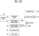
- FIGS. 12A and 12B are diagrams illustrating generating of second operation data by performing an operation on the first operation data in FIG. 8 .
- FIGS. 13A and 13B are diagrams illustrating checking of defects using the second operation data and fixed data in FIG. 8 .
- FIG. 14 is a diagram illustrating a memory system including a memory device according to an embodiment.
- FIG. 15 is a diagram illustrating a memory system including a memory device according to an embodiment.
- FIG. 1 is a diagram illustrating a memory device according to an embodiment of the present disclosure.
- a memory system 1000 may include a memory device 1100 which stores data, and a controller 1200 which performs communication between the memory device 1100 and a host 2000 .
- the memory device 1100 may communicate with the controller 1200 through at least one channel. For example, a command, an address, or data may be transmitted and received through the channel, and the memory device 1100 may be operated in response to the command and the address received through the channel.
- the controller 1200 may perform communication between the host 2000 and the memory device 1100 .
- the controller 1200 may control the memory device 1100 in response to a request from the host 2000 , or may perform a background operation for improving the performance of the memory system 1000 regardless of a request from the host 2000 .
- the host 2000 may generate requests for various operations, and may transmit the generated requests to the memory system 1000 .
- the requests may include a program request for a program operation, a read request for a read operation, an erase request for an erase operation, etc.
- the host 2000 may communicate with the memory system 1000 through various interfaces, such as Peripheral Component Interconnect Express (PCIe), Advanced Technology Attachment (ATA), Serial ATA (SATA), Parallel ATA (PATA), serial attached SCSI (SAS), Non-Volatile Memory Express (NVMe), Universal Serial Bus (USB), Multi-Media Card (MMC), Enhanced Small Disk Interface (ESDI), or Integrated Drive Electronics (IDE).
- PCIe Peripheral Component Interconnect Express
- ATA Advanced Technology Attachment
- SATA Serial ATA
- PATA Parallel ATA
- SAS Serial attached SCSI
- NVMe Non-Volatile Memory Express
- USB Universal Serial Bus
- MMC Multi-Media Card
- ESDI Enhanced Small Disk Interface
- IDE Integrated Drive Electronics
- FIG. 2 is a diagram illustrating a memory device.
- the memory device 1100 may include a CAM block 100 , a page buffer group 110 , an input/output circuit 120 , and a logic circuit 130 .
- the CAM block 100 may be any one of a plurality of memory blocks included in the memory device 1100 , and may store CAM data other than normal data.
- the normal data may be data received from a host (e.g., 2000 of FIG. 1 ), and the CAM data may be system data required for the operation of the memory device 1100 . Therefore, the normal data may be stored in normal memory blocks, and the CAM data may be stored in the CAM block 100 .
- the normal memory blocks may be blocks which can be accessed by a user using an address, and the CAM block 100 may be a block which cannot be accessed by the user using an address.
- the page buffer group 110 may exchange data with the CAM block 100 through bit lines.
- the CAM data read from the CAM block 100 may be temporarily stored in the page buffer group 110 .
- the page buffer group 110 may also be coupled in common to the normal memory blocks through the bit lines.
- the input/output circuit 120 may be coupled to an external device through input/output lines JO.
- the external device may be a controller (e.g., 1200 of FIG. 1 ). Therefore, the input/output lines JO may be included in a channel coupled to the controller 1200 .
- the input/output circuit 120 may transfer the normal data, received from the external device, to the page buffer group 110 , and may transfer the command and the address to the logic circuit 130 . Further, the input/output circuit 120 may output the normal data, received from the page buffer group 110 , to the external device through the input/output lines 10 .
- the logic circuit 130 may output operating voltages to the CAM block 100 or control the page buffer group 110 and the input/output circuit 120 in response to the command received from the input/output circuit 120 or the command and the address received therefrom.
- the logic circuit 130 may include software corresponding to an algorithm that may be executed in response to the command, and may include hardware that may output signals depending on the algorithm.
- the memory device 1100 may include an extra register 61 for the CAM data. For example, when power is supplied to the memory device 1100 and a CAM read command is received from the external device during a boot operation, the memory device 1100 may perform a CAM read operation to use the CAM data stored in the CAM block 100 .
- the CAM read operation may be an operation of reading the CAM data stored in the CAM block 100 and storing the CAM data in the page buffer group 110 . That is, during the normal read operation, after the normal data has been stored in the page buffer group 110 , the normal data is output to the external device through the input/output circuit 120 .
- the CAM data is not transferred to the input/output circuit 120 .
- the CAM data that is read in the CAM read operation may be transmitted to the extra register 61 , and the CAM data stored in the extra register 61 may be used as set values for various operations that are performed by the memory device 1100 . Since the CAM data is data used even in normal memory devices, detailed descriptions thereof are omitted.
- the extra register 61 is included in the logic circuit 130 .
- the extra register 61 will be described as being a component included in the logic circuit 130 .
- the disclosure is not limited thereto. That is, in other embodiments, the extra register 61 may be disposed outside the logic circuit 130 .
- FIG. 3 is a circuit diagram illustrating a CAM block.
- the CAM block 100 may be configured similar to normal memory blocks.
- the CAM block 100 may include a plurality of strings ST coupled between first to m-th bit lines BL 1 to BLm, where m is a positive integer, and a source line SL.
- Each of the strings ST may include a source select transistor SST, first to n-th CAM cells Cl to Cn, and a drain select transistor DST which are coupled in series between the source line SL and a corresponding bit line of the first to m-th bit lines BL 1 to BLm.
- the CAM cells Cl to Cn may be configured similar to normal memory cells included in the normal memory blocks.
- the CAM cells are described as being implemented as NAND memory cells, the structure of the CAM cells according to the present embodiment is not limited to NAND memory cells.
- the strings ST may be respectively coupled to bit lines, and may be coupled in common to the source line SL.
- the numbers of source select transistors SST, first to n-th CAM cells Cl to Cn, and drain select transistors DST are not limited to those illustrated in FIG. 3 .
- Gates of source select transistors SST coupled to different strings ST may be coupled to a source select line SSL, gates of the first to n-th CAM cells Cl to Cn may be coupled to first to n-th word lines WL 1 to WLn, and gates of the drain select transistors DST may be coupled to a drain select line DSL.
- a group of CAM cells which are coupled to the same word line and are included in different strings ST may form one page PG #.
- the CAM cells may be programmed or read on a page PG # basis.
- the first to m-th bit lines BL 1 to BLm may be coupled to respective page buffers included in the page buffer group 110 .
- the storage capacity of the above-described page PG # may be determined depending on the number of CAM cells.
- the storage capacity of the page PG # will be described in detail below.
- FIG. 4 is a diagram illustrating pages included in a CAM block.
- n pages may be included in the CAM block depending on the number of word lines. For example, when the first to n-th word lines are coupled to the CAM block 100 , first to n-th pages PG 1 to PGn may be included in the CAM block 100 .
- the storage capacity of each of the first to n-th pages PG 1 to PGn may be proportional to the number of CAM cells included in the corresponding page. Referring to a part 41 of the first page PG 1 , the storage capacity of each of CAM cells included in different columns may be 1 bit. Therefore, the total capacity of eight CAM cells may be 1 byte, and the first page PG 1 may have a storage capacity of tens to thousands of bytes.
- 1-bit CAM data may be stored in a plurality of CAM cells. That is, the same CAM data may be stored in CAM cells corresponding to 1 byte (1B). For example, when original CAM data is ‘0 1 0 1’, and the same data corresponding to each bit may be stored by 1 byte (1B), the CAM data may be stored as ‘00000000 11111111 00000000 11111111’ in the CAM cells of a selected page.
- the CAM data may be stored in any one of the first to n-th pages PG 1 to PGn, or may be stored in a plurality of pages including one or more erased pages therebetween.
- FIG. 5 is a diagram illustrating a page buffer group.
- the page buffer group 110 may include first to m-th page buffers PB 1 to PBm respectively coupled to first to m-th bit lines BL 1 to BLm.
- Each of the first to m-th page buffers PB 1 to PBm may include a plurality of latches LAT 1 to LATk, where k is a positive integer, which store data.
- the first to m-th page buffers PB 1 to PBm may store data, input from an external device, into a latch selected from among the plurality of latches LAT 1 to LATk, and may adjust the voltages of the first to m-th bit lines BL 1 to BLm depending on the stored data.
- the first to m-th page buffers PB 1 to PBm may sense the voltages or currents of the first to m-th bit lines BL 1 to BLm, and may store data in the latch selected from among the plurality of latches LAT 1 to LATk.
- the first to m-th page buffers PB 1 to PBm may store CAM data, read from the CAM block 100 , in the selected latch, and may then transmit the CAM data, stored in the selected latch, to an extra register (e.g., 61 of FIG. 2 ).
- the extra register 61 and a logic circuit (e.g., 130 of FIG. 2 ) will be described in detail below.
- FIG. 6 is a diagram illustrating a logic circuit according to an embodiment of the present disclosure.
- the logic circuit 130 may include an extra register 61 , a first operation register 62 , a second operation register 63 , a fixed register 64 , core circuits 65 , and an operation logic 66 .
- the extra register 61 may store extra data.
- the extra data may be resulting data obtained by performing a specific operation on items of CAM data stored in the CAM block 100 .
- resulting data obtained by independently performing an XNOR operation on the items of CAM data stored in the CAM block 100 and the items of initial extra data iDext stored in an extra register 61 may be the extra data.
- the extra register 61 may be implemented as a static random access memory (SRAM), a dynamic RAM (DRAM) or a latch.
- the first operation register 62 and the second operation register 63 may be used to store operation values for checking a defect in the extra register 61 .
- the fixed register 64 may store fixed data.
- the fixed data may be data stored in the fixed register 64 at the manufacturing step of the memory device.
- the fixed data may be data that causes the resulting value of a final XOR operation to be ‘0’ in a cyclic redundancy check (CRC) operation that is performed in advance on the CAM data, which is error-free and stored in the CAM block 100 .
- CRC cyclic redundancy check
- the core circuits 65 may include circuits which transmit data among the extra register 61 , the first and second operation registers 62 and 63 , and the fixed register 64 . Also, the core circuit 65 may include circuits that may control the page buffer group 110 and the input/output circuit 120 , illustrated in FIG. 2 , and may generate operating voltages to be applied to word lines coupled to the CAM block.
- the operation logic 66 may control the core circuits 65 in response to a command and an address.
- the operation logic 66 may include software which may perform various operations, for example, a program operation, a read operation or an erase operation, and hardware which may output various control signals for controlling the core circuits 65 depending on the software.
- the operation logic 66 may control the core circuits 65 so that a CAM read operation is performed.
- the operation logic 66 may control the core circuits 65 to check a defect in the CAM data stored in the extra register 61 .
- the operation logic 66 may perform operations on items of data output from the extra register 61 , the page buffer group (e.g., 110 of FIG. 5 ), the first and second operation registers 62 and 63 , and the fixed register 64 , and may determine, based on a final operation value, whether a defect has occurred in the extra register 61 .
- FIG. 7 is a diagram illustrating the storage capacities of storage devices in which data is stored.
- the storage capacity of the extra register 61 may be equal to that of one page (e.g., PG # of FIG. 3 ). In other words, the storage capacity of the extra register 61 may be equal to that of the page buffer group 110 .
- the storage capacity of the first operation register 62 may be less than that of the extra register 61
- the storage capacity of the second operation register 63 may be equal to that of the fixed register 64 .
- the storage capacity of one of the second operation register 63 and the fixed register 64 may be less than that of the extra register 61 and is greater than that of the first operation register 62 .
- the CAM data stored in the page buffer group 110 should be stored in the extra register 61 through a specific operation, and thus the extra register 61 may require the same storage capacity as the page buffer group 110 .
- the extra register 61 may have a storage capacity of a total of 64 bytes (64 B).
- the first operation register 62 may have a storage capacity of 1 byte (1B).
- the second operation register 63 may store resulting data of a CRC operation that uses, e.g., 32 pins, it may have a storage capacity of 4 bytes (4B) corresponding to 32 bits.
- the fixed register 64 may have a storage capacity of 4 bytes (4B), and may store items of fixed data Dfx 1 to Dfx 4 .
- the items of fixed data Dfx 1 to Dfx 4 are items of data that cause the resulting value of a final XOR operation to be ‘0’ in the CRC operation on the CAM data stored in the CAM block 100 at the step of manufacturing the memory device, and are not deleted or changed after they are stored in the fixed register 64 .
- the storage capacity of each of the items of fixed data Dfx 1 to Dfx 4 may be 1 byte (1B).
- the storage capacities of the above-described registers 61 to 64 are mere examples, and the present disclosure is not limited to the storage capacities of the present embodiment.
- FIG. 8 is a flowchart illustrating a method of operating a memory device according to an embodiment of the present disclosure.
- the defect check method according to the present embodiment is schematically illustrated, and detailed methods of respective operations described in FIG. 8 are described through FIGS. 9A to 13B .
- a controller in the memory system 1000 may output a CAM read command for reading a CAM block to a memory device (e.g., 1100 of FIG. 1 ) at operation S 81 .
- the operation logic (e.g., 66 of FIG. 6 ) of the memory device 1100 may read items of CAM data from the CAM block in response to the CAM read command, and may load resulting data, obtained by performing an XNOR operation on the items of read CAM data and the items of initial extra data iDext stored in an extra register 61 , in the extra register (e.g., 61 of FIG. 6 ) at operation S 82 .
- the CAM data loaded in the extra register 61 is defined as extra data Dext.
- the operation logic 66 may read again the items of CAM data from the CAM block and store the CAM data in a page buffer group at operation S 83 .
- the CAM data stored in the page buffer group is defined as page data Dpg.
- the operation logic 66 may generate first operation data Dop 1 by performing a first operation on the extra data Dext stored in the extra register and the page data Dpg stored in the page buffer group at operation S 84 .
- the operation logic 66 may generate the first operation data Dop 1 by performing an XNOR operation on the extra data Dext and the page data Dpg in units of 1 byte.
- the operation logic 66 may generate second operation data Dop 2 by performing a second operation on initial second operation data Dop 2 _int stored in a second operation register 63 and the first operation data Dop 1 at operation S 85 .
- the operation logic 66 may generate final data Dfn by performing an operation on the second operation data Dop 2 and the fixed data Dfx, and may determine whether a defect has occurred in the extra register 61 by checking the final data Dfn at operation S 86 .
- FIGS. 9A and 9B are diagrams illustrating in detail the CAM data loading operation of FIG. 8 , wherein FIG. 9A is a flowchart illustrating in detail the operation S 82 of FIG. 8 and FIG. 9B is a diagram illustrating in detail components which perform operation S 82 .
- the operation logic 66 may perform a CAM read operation on the CAM block 100 by controlling the core circuits 65 in response to a CAM read command at operation S 91 .
- the core circuits 65 may perform the CAM read operation by applying a read voltage to a selected word line of the CAM block.
- CAM data stored in the CAM block 100 is defined as original CAM data Dor.
- the CAM data may be stored in the page buffer group 110 coupled to the CAM block 100 at operation S 92 .
- the core circuits 65 may sense voltages or currents of the bit lines determined depending on the threshold voltages of the CAM cells, and may then store the CAM data in the page buffer group 110 .
- an XNOR operation may be performed on the CAM data stored in the page buffer group 110 and an initial extra data iDext stored in the extra register 61 , and then extra data Dext may be generated at operation S 93 .
- the initial extra data iDext may be input to the extra register 61 during the manufacturing process of a memory device 1100 . Since the extra data Dext is obtained by using the CAM data read from the CAM block 100 and the initial extra data iDext, characteristics of each memory device 1100 can be reflected to the extra data Dext.
- the core circuits 65 may perform the XNOR operation under the control of the operation logic 66 .
- the resulting data obtained from the operation may be the extra data Dext.
- the extra data Dext may be stored in the extra register 61 at operation S 94 .
- the operation logic 66 may reset the page buffer group 110 by controlling the core circuits 65 at operation S 95 .
- the CAM data may be stored in the plurality of page buffers when the CAM read operation is performed. Since each of the plurality of page buffers includes a plurality of latches and CAM data is stored in a latch selected from among the plurality of latches, latches in which CAM data is stored may be reset so that the latches have the same initial data during a reset operation.
- FIGS. 10A and 10B are diagrams illustrating in detail the CAM data read operation of FIG. 8 .
- FIG. 10A is a flowchart illustrating in detail the operation S 83 of FIG. 8
- FIG. 10B is a diagram illustrating in detail components which perform operation S 83 .
- the core circuits 65 may perform again a CAM read operation on the CAM block 100 under the control of the operation logic 66 at operation S 100 .
- the core circuits 65 may perform the CAM read operation by applying a read voltage to a selected word line of the CAM block.
- the core circuits 65 may sense voltages or currents of bit lines, and may then store CAM data in the page buffer group 110 at operation S 101 .
- the CAM data, stored again in the page buffer group 110 is defined as page data Dpg. Therefore, the original CAM data Dor is stored in the CAM block 100 , the page data Dpg read through the CAM read operation is stored in the page buffer group 110 , and extra data Dext is stored in the extra register 61 .
- FIGS. 11A to 11C are diagrams illustrating in detail generating of first operation data by performing an operation on CAM data stored in the extra register and read CAM data in FIG. 8 .
- FIG. 11A is a flowchart illustrating in detail the operation S 84 of FIG. 8
- FIG. 11B is a diagram illustrating in detail components which perform operation S 84
- FIG. 11C is a diagram illustrating in detail the first operation data Dop 1 stored in the first operation register 62 .
- the operation logic 66 may generate 1-byte (1B) first operation data Dop 1 by performing an XNOR operation on 1-byte (1B) extra data Dext and 1-byte (1B) page data Dpg, and may store the first operation data Dop 1 in the first operation register 62 by controlling the core circuits 65 .
- XNOR operation when items of input data are identical to each other, a value of ‘1’ is output, whereas when items of input data are different from each other, a value of ‘0’ is output.
- the core circuits 65 may store the first operation data Dop 1 in the first operation register 62 .
- data obtained by performing an XNOR operation on items of data corresponding to selected addresses of the page buffer group 110 and the extra register 61 may be stored rather than by performing an XNOR operation on all of the page data Dpg and the extra data Dext and storing the results of the XNOR operation.
- resulting data obtained by performing an XNOR operation on items of 1-byte (1B) data corresponding to first addresses of the page buffer group 110 and the extra register 61 may be stored in the first operation register 62 ( ⁇ circle around (1) ⁇ ).
- the resulting data obtained by performing an XNOR operation on items of 1-byte (1B) data corresponding to second addresses of the page buffer group 110 and the extra register 61 may be stored in the first operation register 62 ( ⁇ circle around (1) ⁇ ). In this way, resulting data obtained by sequentially performing XNOR operations on items of data corresponding to respective addresses of the page buffer group 110 and the extra register 61 may be stored in the first operation register 62 .
- FIGS. 12A and 12B are diagrams illustrating in detail generating of second operation data by performing an operation on the first operation data in FIG. 8 , wherein FIG. 12A is a flowchart illustrating in detail the operation S 85 of FIG. 8 and FIG. 12B is a diagram illustrating in detail components which perform operation S 85 .
- the operation logic 66 may generate second operation data Dop 2 by performing an CRC operation on the first operation data Dop 1 and initial second operation data Dop 2 _int.
- the CRC operation is CRC-32 operation.
- the initial second operation data Dop 2 _int may be stored in the second operation register 63 .
- the generated second operation data Dop 2 may be stored in the second operation register 63 .
- the CRC operation may comprise an XOR operation.
- the second operation data Dop 2 may be composed of data values of ‘0’, whereas when the first operation data Dop 1 and the initial second operation data Dop 2 _int are different from each other, the second operation data Dop 2 may be composed of data values of ‘1’.
- FIGS. 13A and 13B are diagrams illustrating in detail checking of defects using the second operation data and fixed data in FIG. 8 , wherein FIG. 13A is a flowchart illustrating in detail the operation S 86 of FIG. 8 , and FIG. 13B is a diagram illustrating in detail components which perform operation S 86 .
- the operation logic 66 may generate final data Dfn by sequentially performing XOR operations on second operation data Dop 2 stored in the second operation register 63 and fixed data Dfx stored in the fixed register 64 at operation S 130 .
- the fixed data Dfx may be data prestored in the fixed register 64 at the manufacturing step of the memory device, and may be data that causes the resulting value of a final XOR operation to be ‘0’ in a cyclic redundancy check (CRC) operation performed in advance on the CAM data, which is error-free when stored in the CAM block 100 .
- CRC cyclic redundancy check
- the operation logic 66 may generate first check data Dck 1 by performing an XOR operation on the second operation data Dop 2 and the first fixed data Dfx 1 , generate second check data Dck 2 by performing an XOR operation on the first check data Dck 1 and the second fixed data Dfx 2 , generate third check data Dck 3 by performing an XOR operation on the second check data Dck 2 and the third fixed data Dfx 3 , and generate final data Dfn by performing an XOR operation on the third check data Dck 3 and the fourth fixed data Dfx 4 .
- the operation logic 66 may determine, based on the final data Dfn, whether a defect has occurred in the extra data at operation S 131 . When it is determined that the final data Dfn has a value of ‘0’, the operation logic 66 may determine that no defect has occurred in the extra data of the selected address at operation S 132 . For example, when data obtained through an operation performed on the extra data of the first address within the extra register 61 is stored in the first and second operation registers 62 and 63 , whether a defect has occurred in the extra data of the first address within the extra register 61 may be determined based on the final data Dfn.
- the defect check operation has passed. This means that no defect has occurred in the extra data of the first address within the extra register 61 .
- the defect check operation has failed. This means that a defect has occurred in the extra data of the first address within the extra register 61 .
- defect check operations may be sequentially performed on the extra data of all addresses within the extra register 61 . Based on the sequentially generated final data Dfn, whether a defect has occurred in the extra data stored in the extra register 61 may be determined, and an address at which a defect has occurred in the extra data stored in the extra register 61 may also be determined.
- the operation logic 66 may output a resulting signal to an external device based on the result of the determination.
- the external device may be the controller (e.g., 1200 of FIG. 1 ) or a test device.
- the memory device e.g., 1100 of FIG. 1
- the extra register 61 may be processed as a fail.
- FIG. 14 is a diagram illustrating a memory system including a memory device according to the present disclosure.
- a memory system 30000 may be implemented as a cellular phone, a smart phone, a tablet PC, a personal digital assistant (PDA) or a wireless communication device.
- the memory system 30000 may include a memory device 1100 and a controller 1200 which is capable of controlling the operation of the memory device 1100 .
- the controller 1200 may control a data access operation for the memory device 1100 , for example, a program operation, an erase operation or a read operation, under the control of a processor 3100 .
- Data programmed to the memory device 1100 may be output via a display 3200 under the control of the controller 1200 .
- a radio transceiver 3300 may exchange radio signals through an antenna ANT.
- the radio transceiver 3300 may convert radio signals received through the antenna ANT into signals that may be processed by the processor 3100 . Therefore, the processor 3100 may process the signals output from the radio transceiver 3300 , and may transmit the processed signals to the controller 1200 or the display 3200 .
- the controller 1200 may transmit the signals processed by the processor 3100 to the memory device 1100 .
- the radio transceiver 3300 may convert signals output from the processor 3100 into radio signals, and output the radio signals to an external device through the antenna ANT.
- An input device 3400 may be used to input a control signal for controlling the operation of the processor 3100 or data to be processed by the processor 3100 .
- the input device 3400 may be implemented as a pointing device such as a touch pad, a computer mouse, a keypad or a keyboard.
- the processor 3100 may control the operation of the display 3200 so that data output from the controller 1200 , data output from the radio transceiver 3300 , or data output from the input device 3400 is output via the display 3200 .
- the controller 1200 that is capable of controlling the operation of the memory device 1100 may be implemented as a part of the processor 3100 or as a chip provided separately from the processor 3100 .
- FIG. 15 is a diagram illustrating a memory system including a memory device according to the present disclosure.
- a memory system 70000 may be implemented as a memory card or a smart card.
- the memory system 70000 may include a memory device 1100 , a controller 1200 , and a card interface 7100 .
- the controller 1200 may control data exchange between the memory device 1100 and the card interface 7100 .
- the card interface 7100 may be, but is not limited to, a secure digital (SD) card interface or a multi-media card (MMC) interface.
- SD secure digital
- MMC multi-media card
- Data programmed to the memory device 1100 may be output via the card interface 7100 under the control of the controller 1200 .
- the card interface 7100 may interface data exchange between a host 60000 and the controller 1200 according to a protocol of the host 60000 .
- the card interface 7100 may support a universal serial bus (USB) protocol and an interchip (IC)-USB protocol.
- USB universal serial bus
- IC interchip
- the card interface 7100 may refer to hardware capable of supporting a protocol which is used by the host 60000 , software installed in the hardware, or a signal transmission method supported by the card interface 7100 .
- the host interface 6200 may perform data communication with the memory device 1100 through the card interface 7100 and the controller 1200 under the control of a microprocessor ( ⁇ P) 6100 .
- ⁇ P microprocessor
- the present disclosure may check defects, occurring in an extra register into which data in a CAM block is loaded, within a memory device, thus improving the reliability of the memory device.
Landscapes
- Engineering & Computer Science (AREA)
- Theoretical Computer Science (AREA)
- General Engineering & Computer Science (AREA)
- General Physics & Mathematics (AREA)
- Physics & Mathematics (AREA)
- Quality & Reliability (AREA)
- Human Computer Interaction (AREA)
- Microelectronics & Electronic Packaging (AREA)
- Computer Hardware Design (AREA)
- Computer Security & Cryptography (AREA)
- Read Only Memory (AREA)
- For Increasing The Reliability Of Semiconductor Memories (AREA)
- Techniques For Improving Reliability Of Storages (AREA)
Abstract
Description
Claims (21)
Applications Claiming Priority (2)
| Application Number | Priority Date | Filing Date | Title |
|---|---|---|---|
| KR10-2020-0032780 | 2020-03-17 | ||
| KR1020200032780A KR102675508B1 (en) | 2020-03-17 | 2020-03-17 | Memory device and operating method thereof |
Publications (2)
| Publication Number | Publication Date |
|---|---|
| US20210295896A1 US20210295896A1 (en) | 2021-09-23 |
| US11227652B2 true US11227652B2 (en) | 2022-01-18 |
Family
ID=77677368
Family Applications (1)
| Application Number | Title | Priority Date | Filing Date |
|---|---|---|---|
| US16/997,432 Active US11227652B2 (en) | 2020-03-17 | 2020-08-19 | Memory device and method of operating the same |
Country Status (3)
| Country | Link |
|---|---|
| US (1) | US11227652B2 (en) |
| KR (1) | KR102675508B1 (en) |
| CN (1) | CN113407109B (en) |
Families Citing this family (3)
| Publication number | Priority date | Publication date | Assignee | Title |
|---|---|---|---|---|
| US12423375B2 (en) * | 2021-10-15 | 2025-09-23 | Macronix International Co., Ltd. | Memory device and computing method thereof |
| CN114398013B (en) * | 2022-01-26 | 2024-06-18 | 东芯半导体股份有限公司 | NAND memory security code generation module and generation method, and NAND memory |
| CN114649049B (en) * | 2022-03-23 | 2025-08-29 | 东芯半导体股份有限公司 | CAM unit inspection module and inspection method thereof |
Citations (3)
| Publication number | Priority date | Publication date | Assignee | Title |
|---|---|---|---|---|
| US20140241059A1 (en) * | 2013-02-22 | 2014-08-28 | Elpida Memory, Inc. | Method and device for storing and reading reliable information in a nand array |
| KR101486424B1 (en) | 2008-09-12 | 2015-01-26 | 삼성전자주식회사 | An error correction circuit, a flash memory system having an error correction circuit, and an operation method of an error correction circuit |
| US9891976B2 (en) | 2015-02-26 | 2018-02-13 | Arm Limited | Error detection circuitry for use with memory |
Family Cites Families (13)
| Publication number | Priority date | Publication date | Assignee | Title |
|---|---|---|---|---|
| US6034891A (en) * | 1997-12-01 | 2000-03-07 | Micron Technology, Inc. | Multi-state flash memory defect management |
| US6597595B1 (en) * | 2001-08-03 | 2003-07-22 | Netlogic Microsystems, Inc. | Content addressable memory with error detection signaling |
| US7296210B2 (en) * | 2003-09-16 | 2007-11-13 | Alcatel-Lucent Inc | Facilitating error detection for content addressable memory |
| KR100518599B1 (en) * | 2003-11-03 | 2005-10-04 | 삼성전자주식회사 | CAM(Content Addressable Memory) capable of finding errors in priority encoder and method thereof |
| US8103936B2 (en) * | 2007-10-17 | 2012-01-24 | Micron Technology, Inc. | System and method for data read of a synchronous serial interface NAND |
| KR20100085657A (en) * | 2009-01-21 | 2010-07-29 | 주식회사 하이닉스반도체 | Non volatile memory device and method of operating the same |
| US8023298B1 (en) * | 2010-02-19 | 2011-09-20 | Netlogic Microsystems, Inc. | Encoding data for storage in a content addressable memory |
| KR20120013538A (en) * | 2010-08-05 | 2012-02-15 | 주식회사 하이닉스반도체 | Semiconductor memory device and operation method thereof |
| US9899102B2 (en) * | 2015-03-31 | 2018-02-20 | SK Hynix Inc. | Semiconductor device and operating method thereof |
| KR20170090177A (en) * | 2016-01-28 | 2017-08-07 | 에스케이하이닉스 주식회사 | Memory system, semiconductor memory device and operating method thereof |
| CN108735268B (en) * | 2017-04-19 | 2024-01-30 | 恩智浦美国有限公司 | Nonvolatile memory repair circuit |
| KR20190021869A (en) * | 2017-08-24 | 2019-03-06 | 에스케이하이닉스 주식회사 | Memory system and operating method thereof |
| US10984863B2 (en) * | 2018-04-20 | 2021-04-20 | Arm Limited | Error detection and correction circuitry |
-
2020
- 2020-03-17 KR KR1020200032780A patent/KR102675508B1/en active Active
- 2020-08-19 US US16/997,432 patent/US11227652B2/en active Active
- 2020-10-12 CN CN202011083276.2A patent/CN113407109B/en active Active
Patent Citations (3)
| Publication number | Priority date | Publication date | Assignee | Title |
|---|---|---|---|---|
| KR101486424B1 (en) | 2008-09-12 | 2015-01-26 | 삼성전자주식회사 | An error correction circuit, a flash memory system having an error correction circuit, and an operation method of an error correction circuit |
| US20140241059A1 (en) * | 2013-02-22 | 2014-08-28 | Elpida Memory, Inc. | Method and device for storing and reading reliable information in a nand array |
| US9891976B2 (en) | 2015-02-26 | 2018-02-13 | Arm Limited | Error detection circuitry for use with memory |
Also Published As
| Publication number | Publication date |
|---|---|
| CN113407109A (en) | 2021-09-17 |
| US20210295896A1 (en) | 2021-09-23 |
| KR20210116077A (en) | 2021-09-27 |
| CN113407109B (en) | 2024-06-14 |
| KR102675508B1 (en) | 2024-06-17 |
Similar Documents
| Publication | Publication Date | Title |
|---|---|---|
| US11068408B2 (en) | Memory system and operating method thereof | |
| US11309050B2 (en) | Memory controller and memory system having the same | |
| US11294814B2 (en) | Memory system having a memory controller and a memory device having a page buffer | |
| US20120203959A1 (en) | Non-volatile memory, system including the same, and method of programming the same | |
| US11227652B2 (en) | Memory device and method of operating the same | |
| US10678471B2 (en) | Memory controller, memory system having the memory controller, and operating method of the memory controller | |
| US10621036B2 (en) | Memory system and operation method thereof | |
| US10490238B2 (en) | Serializer and memory device including the same | |
| US20190278716A1 (en) | Memory controller and operating method thereof | |
| US11080134B2 (en) | Memory controller and memory system including the same | |
| CN111105833B (en) | Memory device, memory system and method of operating a memory system | |
| KR20190073125A (en) | Memory system and operating method thereof | |
| US11132252B2 (en) | Memory device, memory system including memory device, and method of operating memory system | |
| US10942675B2 (en) | Memory system and operating method thereof | |
| US11403038B2 (en) | Controller, a memory system including the controller, and method of operating the controller | |
| US12512163B2 (en) | Memory device and operating method of memory device | |
| US12292825B2 (en) | Memory control method, memory storage device and memory control circuit unit | |
| TW202526953A (en) | Dummy data-based read reference voltage search of nand memory | |
| KR20190041698A (en) | Memory controller and memory system having the same |
Legal Events
| Date | Code | Title | Description |
|---|---|---|---|
| AS | Assignment |
Owner name: SK HYNIX INC., KOREA, REPUBLIC OF Free format text: ASSIGNMENT OF ASSIGNORS INTEREST;ASSIGNORS:KIM, SUN HAK;HONG, YONG HWAN;KIM, BYUNG RYUL;AND OTHERS;REEL/FRAME:053541/0261 Effective date: 20200805 |
|
| FEPP | Fee payment procedure |
Free format text: ENTITY STATUS SET TO UNDISCOUNTED (ORIGINAL EVENT CODE: BIG.); ENTITY STATUS OF PATENT OWNER: LARGE ENTITY |
|
| STPP | Information on status: patent application and granting procedure in general |
Free format text: NON FINAL ACTION MAILED |
|
| STPP | Information on status: patent application and granting procedure in general |
Free format text: RESPONSE TO NON-FINAL OFFICE ACTION ENTERED AND FORWARDED TO EXAMINER |
|
| STPP | Information on status: patent application and granting procedure in general |
Free format text: NOTICE OF ALLOWANCE MAILED -- APPLICATION RECEIVED IN OFFICE OF PUBLICATIONS |
|
| STPP | Information on status: patent application and granting procedure in general |
Free format text: PUBLICATIONS -- ISSUE FEE PAYMENT VERIFIED |
|
| STCF | Information on status: patent grant |
Free format text: PATENTED CASE |
|
| MAFP | Maintenance fee payment |
Free format text: PAYMENT OF MAINTENANCE FEE, 4TH YEAR, LARGE ENTITY (ORIGINAL EVENT CODE: M1551); ENTITY STATUS OF PATENT OWNER: LARGE ENTITY Year of fee payment: 4 |