US11226768B2 - Memory controller and method for accessing memory module - Google Patents
Memory controller and method for accessing memory module Download PDFInfo
- Publication number
- US11226768B2 US11226768B2 US15/950,174 US201815950174A US11226768B2 US 11226768 B2 US11226768 B2 US 11226768B2 US 201815950174 A US201815950174 A US 201815950174A US 11226768 B2 US11226768 B2 US 11226768B2
- Authority
- US
- United States
- Prior art keywords
- data
- access command
- buffer
- access
- processing
- Prior art date
- Legal status (The legal status is an assumption and is not a legal conclusion. Google has not performed a legal analysis and makes no representation as to the accuracy of the status listed.)
- Active
Links
Images


Classifications
-
- G—PHYSICS
- G06—COMPUTING; CALCULATING OR COUNTING
- G06F—ELECTRIC DIGITAL DATA PROCESSING
- G06F3/00—Input arrangements for transferring data to be processed into a form capable of being handled by the computer; Output arrangements for transferring data from processing unit to output unit, e.g. interface arrangements
- G06F3/06—Digital input from, or digital output to, record carriers, e.g. RAID, emulated record carriers or networked record carriers
- G06F3/0601—Interfaces specially adapted for storage systems
- G06F3/0628—Interfaces specially adapted for storage systems making use of a particular technique
- G06F3/0655—Vertical data movement, i.e. input-output transfer; data movement between one or more hosts and one or more storage devices
- G06F3/0659—Command handling arrangements, e.g. command buffers, queues, command scheduling
-
- G—PHYSICS
- G06—COMPUTING; CALCULATING OR COUNTING
- G06F—ELECTRIC DIGITAL DATA PROCESSING
- G06F13/00—Interconnection of, or transfer of information or other signals between, memories, input/output devices or central processing units
- G06F13/14—Handling requests for interconnection or transfer
- G06F13/16—Handling requests for interconnection or transfer for access to memory bus
- G06F13/1668—Details of memory controller
- G06F13/1673—Details of memory controller using buffers
-
- G—PHYSICS
- G06—COMPUTING; CALCULATING OR COUNTING
- G06F—ELECTRIC DIGITAL DATA PROCESSING
- G06F12/00—Accessing, addressing or allocating within memory systems or architectures
- G06F12/02—Addressing or allocation; Relocation
- G06F12/08—Addressing or allocation; Relocation in hierarchically structured memory systems, e.g. virtual memory systems
-
- G—PHYSICS
- G06—COMPUTING; CALCULATING OR COUNTING
- G06F—ELECTRIC DIGITAL DATA PROCESSING
- G06F3/00—Input arrangements for transferring data to be processed into a form capable of being handled by the computer; Output arrangements for transferring data from processing unit to output unit, e.g. interface arrangements
- G06F3/06—Digital input from, or digital output to, record carriers, e.g. RAID, emulated record carriers or networked record carriers
- G06F3/0601—Interfaces specially adapted for storage systems
- G06F3/0602—Interfaces specially adapted for storage systems specifically adapted to achieve a particular effect
- G06F3/0604—Improving or facilitating administration, e.g. storage management
-
- G—PHYSICS
- G06—COMPUTING; CALCULATING OR COUNTING
- G06F—ELECTRIC DIGITAL DATA PROCESSING
- G06F3/00—Input arrangements for transferring data to be processed into a form capable of being handled by the computer; Output arrangements for transferring data from processing unit to output unit, e.g. interface arrangements
- G06F3/06—Digital input from, or digital output to, record carriers, e.g. RAID, emulated record carriers or networked record carriers
- G06F3/0601—Interfaces specially adapted for storage systems
- G06F3/0628—Interfaces specially adapted for storage systems making use of a particular technique
- G06F3/0655—Vertical data movement, i.e. input-output transfer; data movement between one or more hosts and one or more storage devices
- G06F3/0656—Data buffering arrangements
-
- G—PHYSICS
- G06—COMPUTING; CALCULATING OR COUNTING
- G06F—ELECTRIC DIGITAL DATA PROCESSING
- G06F3/00—Input arrangements for transferring data to be processed into a form capable of being handled by the computer; Output arrangements for transferring data from processing unit to output unit, e.g. interface arrangements
- G06F3/06—Digital input from, or digital output to, record carriers, e.g. RAID, emulated record carriers or networked record carriers
- G06F3/0601—Interfaces specially adapted for storage systems
- G06F3/0668—Interfaces specially adapted for storage systems adopting a particular infrastructure
- G06F3/0671—In-line storage system
- G06F3/0673—Single storage device
Definitions
- the application generally relates to memory technology, and more particularly to a memory controller and a method for accessing a memory module.
- a memory module group provides data access and storage during computations of a central processing unit (CPU).
- CPU central processing unit
- the memory module group may use a controller chip with a buffering function to buffer operation commands sent from the CPU and the corresponding memory addresses, and the memory module group further comprises a data buffer that can bidirectionally buffer data.
- the operation mode of the existing memory module group is relatively simple, and only supports simple operations such as reading and writing, which limits the functions of the memory module group. Therefore, it is necessary to improve the data access method of the existing memory module group.
- One objective of the application is to provide a memory controller and a method for accessing a memory module, which can implement complex data access operations.
- a memory controller is provided.
- the memory controller is coupled between a memory module and a host controller to control access of the host controller to the memory module.
- the memory controller comprises: a central buffer coupled to the host controller for receiving a data access command from the host controller, and coupled to the memory module for providing a modified data access command to the memory module; wherein the central buffer comprises an access command processing module configured for processing the data access command to generate the modified data access command; and a data buffer coupled to the central buffer for receiving the modified data access command from the central buffer, and coupled between the host controller and the memory module for exchanging data between the host controller and the memory module under the control of the modified data access command.
- processing the data access command via the access command processing module comprises: encoding an access address in the data access command such that the modified data access command includes an encoded access address.
- processing the data access command via the access command processing module comprises: processing an access address in the data access command with a predefined address processing algorithm to generate a set of access addresses based on the access address, wherein each access address in the set of access addresses corresponds to a modified data access command.
- the set of access addresses comprises multiple consecutive access addresses in an ascending or descending order.
- the set of access addresses comprises multiple nonconsecutive access addresses at equal intervals or at unequal intervals.
- the modified data access command is of an access type identical to that of the data access command.
- the data buffer comprises a data processing module configured for receiving data from the host controller or the memory module, processing the data with a predefined data processing algorithm, and sending the processed data to the host controller or the memory module.
- the data buffer comprises a data processing module configured for receiving data from the memory module, processing the data with a predefined data processing algorithm, and sending the processed data to the memory module.
- processing the data access command via the access command processing module comprises: processing an access address in the data access command with a predefined address processing algorithm to generate a set of access addresses based on the access address, wherein each access address in the set of access addresses corresponds to a modified data access command;
- the data buffer comprises a data processing module configured for receiving data from the memory module according to the modified data access command, processing the data with a predefined data processing algorithm, and sending the processed data to the memory module according to the modified data access command.
- the data buffer comprises multiple data buffer units, each of the data buffer units corresponding to a data processing sub-module, wherein the multiple data processing sub-modules are coupled to each other to exchange data between the multiple data buffer units.
- the memory module and the memory controller are in accordance with the JEDEC DDR SDRAM standard
- the central buffer is integrated in a registering clock driver
- the registering clock driver is coupled to the data buffer via a data buffer control bus.
- a memory device comprises the memory controller and the memory module of the abovementioned aspect.
- a computer system is further provided.
- the computer system comprises the memory device of the abovementioned aspect.
- a method for accessing a memory module is provided.
- the memory module is coupled to a host controller via a memory controller, and the memory controller comprises a data buffer and a central buffer, the central buffer comprising an access command processing module, wherein the access command processing module is configured for processing a data access command to generate a modified data access command;
- the method comprises: receiving, via the central buffer, a data access command; processing, via the central buffer, the data access command to generate a modified data access command; providing, via the central buffer, the modified data access command to the memory module and the data buffer; exchanging, via the data buffer, data between the host controller and the memory module according to the modified data access command.
- FIG. 1 shows a memory system 100 according to an embodiment of the application.
- FIG. 2 shows an exemplary sequence diagram of a data processing operation instructed by a BCOM bus.
- FIG. 3 shows an example of block operations using a memory controller according to an embodiment of the application.
- FIG. 4 shows an exemplary structure of a central buffer 400 according to an embodiment of the application.
- FIG. 5 shows an exemplary structure of a data buffer 500 according to an embodiment of the application
- FIG. 6 shows a method 600 for accessing a memory module according to an embodiment of the application.
- FIG. 1 shows a memory system 100 according to an embodiment of the application.
- the memory system 100 comprises a memory module 102 which is configured as a memory module group in the present embodiment, for storing data.
- the memory module 102 may be a memory module in accordance with the JEDEC Double Data Rate (DDR) Synchronous Dynamic Random Access Memory (SDRAM) standard, including, for example, the JEDEC DDR, DDR2, DDR3, DDR4 and other DDR standards.
- the memory module 102 can be an internal memory in accordance with other standards or protocols, e.g. a SDRAM or RAMBUS internal memory.
- the memory module 102 may comprise a volatile memory (e.g., RAM), a non-volatile memory (e.g., flash memory) or a combination thereof. It should be noted that the memory module 102 herein may be a memory chip of a single die or a memory chip of two or more dies.
- the memory system 100 can further comprise a memory controller 104 , and the memory controller 104 comprises a central buffer 106 and a data buffer (DB_P) 108 .
- the central buffer 106 is coupled between a host controller 110 and the memory module 102 , and can receive a data access command containing an access address and an access type from the host controller 110 .
- the data access command may be a command of accessing (e.g., reading or writing) a data storing address (i.e., the access address) in the memory module 102 .
- the data buffer 108 is coupled between the memory module 102 and the host controller 110 , for exchanging data between the memory module 102 and the host controller 110 under the control of the central buffer 106 .
- the central buffer can be integrated in a registering clock driver (RCD).
- the central buffer is coupled to the host controller 110 via a command/address (C/A) bus, e.g. a bus DCA shown in FIG. 1 , to receive a data access command.
- the C/A bus may comprise pins A 0 -A 17 , pins BG 0 -BG 1 and/or pins BA 0 -BA 1 .
- the pins BG 0 -BG 1 are for determining which memory bank group in the memory module 102 is to be processed, e.g. being written into or being read from.
- the pins BA 0 -BA 1 are for determining which memory bank in the memory module 102 is to be processed, and the pins A 0 -A 17 are for addressing and determining which memory unit in a memory bank is to be processed.
- input to the three pins A 16 (RAS_n), A 15 (CAS_n) and A 14 (WE_n) can be used for identifying an input data access command, such as a read command, a write command or other predefined control commands.
- the central buffer 106 has an access command processing module (CA_P) 112 , which can be constructed as a module having data processing and operating ability.
- the access command processing module 112 can be implemented by software, hardware, firmware or a combination thereof.
- the access command processing module 112 can be an application specific integrated circuit or a field programmable logic array chip.
- the access command processing module 112 can process a data access command received from the host controller 110 , so as to generate a modified data access command.
- the access command processing module 112 can provide the modified data access command to the memory module 102 and the data buffer 108 , such that the two can continue performing data access operations according to the modified data access command.
- the access command processing module 112 can generate one or more access addresses according to the access address contained in the data access command, and these access addresses can be provided to the memory module 102 for addressing during data accessing.
- a bus QCA is configured between the memory module 102 and the central buffer 106 for signal and command interaction therebetween.
- the access command processing module 112 also generates a corresponding access type according to the access type of the data access command, such that the data buffer 108 can control the data exchange between the accessed memory unit in the memory module 102 and the host controller 110 according to the generated access type.
- the access command processing module 112 can generate a modified data access command in any desired manner.
- the access command processing module can encode an access address in the data access command, such that the modified data access command includes an encoded access address.
- the access command processing module may process an access address in the data access command with a predefined address processing algorithm, so as to generate a set of access addresses based on the original access address. Each access address of the newly generated set of access addresses can correspond to a modified data access command.
- these modified data access commands may be of an access type identical to that of the original data access commands.
- the data access command received from the host controller 110 may be a data access command for reading an access address in the memory module 102 , so the newly generated modified data access command can be a data access command for reading multiple access addresses related to the access address.
- a set of access addresses in the set of modified data access commands may include multiple consecutive access addresses in an ascending or descending order, wherein the set of access addresses can use a received access address as an initial address.
- the host controller 110 only needs to provide one data access command to the memory controller 104 to access multiple memory units in the memory module 102 , which significantly improves the efficiency of the data accessing.
- the set of access addresses may include multiple non-consecutive access addresses at equal intervals, wherein the interval can be 1, 2 or other natural numbers.
- the set of access addresses substantially corresponds to a column of memory units in the memory array (or at least a part of a column of memory units). For many vector-operations, this column-by-column access can significantly improve the operation efficiency.
- the set of access addresses may include multiple non-consecutive access addresses at unequal intervals. The intervals between these access addresses can be configured according to the data required by actual vector-operations.
- the access address sequence corresponds to the memory units on a diagonal of the memory array
- the set of access addresses substantially correspond to accessing the memory units on the diagonal of the memory array, and this data access method is beneficial to many types of vector-operations and other operations or calculations.
- the access command processing module 112 can encrypt an access address in a data access command with an encryption algorithm, such that the encrypted access address is different from the access address in plaintext. For example, a memory address of the encrypted data is different from a data memory address provided by the host controller.
- the access address included in a read command can be decrypted by the access command processing module 112 , such that the requested data can be read out from the corresponding location of the memory module.
- a data processing module (D_P) 114 is included in the data buffer 108 .
- the data processing module 114 can receive data from the host controller 110 and the memory module 102 to which it is coupled, process the received data with a predefined data processing algorithm, and then send the processed data to the host controller 110 and the memory module 102 .
- the data buffer 108 can buffer the data received from the memory module 102 , and process the data via the data processing module 114 .
- the data obtained by the host controller 110 are processed data.
- the data buffer 108 can also buffer data received from the host controller 110 , process the data via the data processing module 114 , and then write the data into the memory module 102 .
- the data stored in the memory module 102 is processed data.
- the data processing module 114 can receive data from the memory module 102 and process the data, so as to send the processed data to the memory module 102 .
- data can be directly processed in the memory controller 104 without being transferred to the host controller 110 , which significantly reduces the volume of the data exchanged between the host controller 110 and the memory module 102 and improves the data processing efficiency.
- the data processing performed by the data processing module 114 may include various bitwise operations.
- these bitwise operations may include: bit-left-shift, bit-right-shift, bit-left-rotate, bit-right-rotate, bit-and, bit-or, bit-xor, bit-nxor, bit-clear, bit-set or other similar operations.
- the data processing module 114 can perform various types of data operations, such as XCHG (exchange), MOV (move), INC (increment), DEC (decrement) or other similar operations.
- the data processing module 114 may also perform an encryption/decryption process with an encryption/decryption algorithm to ensure the security of the data stored in the memory module and the security of the data transmission between the host controller and the memory module.
- the encryption/decryption process can be, for example, encrypting data when writing it into the memory module or decrypting data when reading it from the memory module.
- the data buffer 108 may comprise multiple data buffer units 108 i , and each data buffer unit 108 i corresponds to a data processing sub-module 114 i .
- each different data processing sub-module 114 i is coupled to each other through bidirectional interfaces BOP (such as BOP 01 , BOP 12 . . . B 0 P 67 and BOP 70 in FIG. 1 ), so as to exchange data among the multiple data buffer units 108 i .
- BOP such as BOP 01 , BOP 12 . . . B 0 P 67 and BOP 70 in FIG. 1
- Exchanging data between different data buffer units 108 i can satisfy requirements of various operations, such as bit-shift, bit-rotate, INC, DEC and so on.
- the BOP interfaces may have a two-wire bidirectional bus structure, including a clock line and a 1-bit bidirectional data line, and perform bidirectional data exchange through agreed protocols.
- the interfaces may have a three-wire bus structure, including a clock line, a transmission direction indication signal line, and a 1-bit bidirectional data line. The bandwidth of the BOP interfaces can be increased by increasing the number of bidirectional data lines.
- the data processing module 114 can respond to an operation command provided by the central buffer 106 .
- the operation command may be transmitted through the data buffer control bus (BCOM) between the central buffer 106 and the data buffer 108 .
- BCOM data buffer control bus
- the data buffer control bus can be 4-bit wide. Table 1 shows an example of the operation commands that can be provided via the BCOM bus.
- Operation Command List BCOM[3:0] Encoding (OP) Operation Command 0000 Normal read 0001 Bit-left-shift 0010 Bit-right-shift 0011 Bit-left-rotate 0100 Bit-right-rotate 0101 Bit-and 0110 Bit-or 0111 Bit-xor 1000 Bit-nxor 1001 Bit-clear 1010 Bit-set 1011 XCHG 1100 MOV 1101 INC 1110 DEC 1111 RFU (Reserved for Future Use)
- FIG. 2 shows an exemplary timing diagram of a data processing operation instructed via the BCOM bus. As shown in FIG. 2 , codes of OPs are added on the BCOM bus to indicate the corresponding data processing operations.
- the memory controller may only include one of them in practical applications.
- the memory controller may only include the access command processing module 112 to generate a modified data access command, and the modified data access command can instruct the data buffer 108 not to process the data but to perform the normal operations such as read, write, etc.
- the memory controller may only include the data processing module 114 to process the buffered data as instructed by the central buffer via the BCOM bus.
- the memory controller 100 shown in FIG. 1 can implement various complex data processing operations. These complex access operations performed by the access command processing module can be triggered in different ways according to different embodiments. In an embodiment, these complex access operations can be instructed by a bit in the command/address bus which is unused (or reserved) in the memory module specification. In some other embodiments, a trigger address (e.g., a memory address in the memory module) can be stored in the access command processing module in advance. When the central buffer receives a data access command including (or with) the trigger address, the complex access operation is triggered. In some other embodiments, whether to trigger a complex access operation can be indicated by inserting the corresponding code one clock cycle before the data access command of the memory module.
- a trigger address e.g., a memory address in the memory module
- FIG. 3 shows an example of using a memory controller for block operations according to an embodiment of the application.
- a memory module includes a memory array 302 , wherein memory units 304 of the memory array 302 are arranged in an array.
- the memory array 302 may include multiple memory blocks, wherein each memory block may include, for example, 4096 memory units.
- the addresses of the memory units in the same memory block can be consecutive, for example, the addresses start at addr 0 and end at addr 4095 .
- complex block operations can be performed by using the memory controller in the embodiments of the application.
- the host controller can send a data access command (read operation) to the memory controller, which includes the start address addr 0 of the memory block.
- the memory controller can obtain the start address addr 0 and generate a set of access addresses based on the start address addr 0 .
- the set of access addresses can include a total of 4096 access addresses from the start address addr 0 to the end address addr 4095 .
- the memory controller can generate 4096 modified data access commands, and these modified data access commands are sent to the memory module and the data buffer.
- the data buffer correspondingly receives and buffers the data stored in these addresses, and provides the data to the host controller. It can be seen that, during the entire data reading process, the host controller only needs to provide one data access command to the memory controller to read the data of 4096 memory units in a block, which significantly improves data reading efficiency. It should be noted that, the number of the memory units accessed in the abovementioned block operation is merely exemplary. In practical applications, any number of memory units can be processed.
- the abovementioned block-read operation does not use the data processing module in the data buffer.
- complex block operations can be performed using the data processing module either.
- a “block-modify” operation can be performed on the memory block in the memory array shown in FIG. 3 .
- the host controller can send a data access command (block-modify operation) to the memory controller, which includes the start address addr 0 of the memory block.
- the memory controller can obtain the start address addr 0 and generate a set of access addresses based on the start address addr 0 .
- the set of access addresses includes a total of 4096 access addresses from the start address to the end address addr 4095 .
- the memory controller can generate 4096 data read commands, and these data read commands are sent to the memory module and the data buffer. Then, the data buffer correspondingly receives and buffers the data stored in these access addresses.
- the modified data access commands corresponding to the block-modify operation can also include an operation of instructing the data processing module in the data buffer to perform a relevant data processing operation (except for the foregoing data read operation).
- the data processing operation can include a bit-and or bit-left-rotate operation on the read data, and a further operation to write the processed data back into the corresponding memory units (or continue buffering the processed data in the data buffer).
- the host controller only needs to provide a block-modify command to modify the data stored in all memory units in the whole block. It will be understood that, during the foregoing block-modify operation process, the data processed by the data processing module can also be provided to the host controller instead of being written back into the memory module.
- the data processing module 114 can perform a read-process-write operation on a memory unit.
- the read-process-write operation refers to an operation that after the host controller initializes a read operation, data processing is performed on the read data out from the memory module according to requirements, and then the process data is directly written back into the memory module via the memory controller.
- the access command processing module of the central buffer may notify the corresponding data processing module to perform, for example, a bit logic operation or a data operation, according a preset processing flow (see Table 1). After the bit logic operation or data operation is completed, the “read-process-write” operation is completed, and the access command processing module can control to write the data back to the memory module so as to complete the whole “read-process-write” operation.
- FIG. 4 shows an exemplary structure of a central buffer 400 according to an embodiment of the application.
- the central buffer 400 comprises two signal paths coupled between a receiving side (D side) and an output side (Q side), being a buffer 402 and an access command processing module 404 respectively.
- a receiving side D side
- Q side output side
- the buffer 402 For a path of the buffer 402 , after receiving the data access command (CMD&ADDR) containing an access address and an access type, the buffer 402 does not perform additional process on the data access command but merely buffers this command and then outputs it from the output side.
- the access command processing module 404 comprises an operating module 406 and a control unit 408 .
- the access command processing module 404 After receiving the data access command sent from the host control module (not shown), the access command processing module 404 determines whether address processing and corresponding operation command generation, i.e., modifying the data access command, are needed based on a predefined triggering condition. After the triggering condition is satisfied, the access command processing module 404 modifies the command via the operating module 406 , and generates a modified data access command. Then, the control unit 408 switches the output of the central buffer 400 from the output of the buffer 402 to the output of the access command processing module 404 through a multiplexer (MUX), and simultaneously sends a corresponding control signal to each data processing module (not shown in the figure) of the data buffer via the BCOM bus, so as to instruct these data processing modules to perform corresponding data processing operations.
- MUX multiplexer
- the buffer 402 and the access command processing module 404 can be configured with the configuration information stored in the register table, and the configuration information of the register table can be modified via the SMBus interface.
- FIG. 5 shows an exemplary structure of a data buffer 500 according to an embodiment of the application
- the data buffer 500 comprises two signal paths coupled between a host controller side and a memory module side, respectively via a bidirectional buffer 502 and a data processing module 504 .
- the data processing module 504 comprises an operating unit 506 and a control unit 508 , wherein the operating unit 506 further exchanges data with a data processing module of an adjacent data buffer through a BOP interface.
- the operating unit 506 can perform a corresponding operation on data based on the control command received by the control unit 508 from the BCOM bus.
- the data processing module 504 can exchange data with adjacent data buffers via the BOP interfaces, wherein the BOP_L interface is for exchanging data with data buffers on the left side, and the BOP_R interface is for exchanging data with data buffers on the right side.
- the bidirectional buffer 502 and the data processing module 504 can be configured with the configuration information stored in the register table.
- circuit architectures of the central buffer and the data buffers shown in FIG. 4 and FIG. 5 are merely exemplary, and changes can be made to these circuit configurations based on needs in practical applications.
- the memory controllers of the embodiments of the application can be applied in memory devices or systems, and such memory devices and systems can be used in various computer systems.
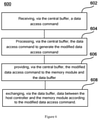
- FIG. 6 shows a method 600 for accessing a memory module according to an embodiment of the application.
- the method 600 can be executed by, for example, the memory controller shown in FIG. 1 .
- the method 600 may comprise step 602 of receiving a data access command via the central buffer; step 604 of processing the data access command to generate a modified data access command via the central buffer; step 606 of providing the modified data access command to the memory module and the data buffer via the central buffer; and step 608 of exchanging data between the host controller and the memory module according to the modified data access command via the data buffer.
- the step 604 may include: encoding an access address in the data access command such that the modified data access command contains an encoded access address.
- the step 604 may include: processing an access address in the data access command with a predefined address processing algorithm to generate a set of access addresses based on the access address, wherein each access address in the set of access addresses corresponds to a modified data access command.
- the set of access addresses includes multiple consecutive access addresses in an ascending or descending order.
- the set of access addresses includes multiple non-consecutive access addresses at equal intervals or at unequal intervals.
- the modified data access command is of an access type identical to that of the data access command.
- the step 608 may include: receiving data from the memory module, processing the data with a predefined data processing algorithm, and sending the processed data to the memory module via the data buffer according to the modified data access command.
Abstract
Description
| TABLE 1 |
| Operation Command List |
| BCOM[3:0] Encoding | |
| (OP) | Operation Command |
| 0000 | Normal read |
| 0001 | Bit-left-shift |
| 0010 | Bit-right-shift |
| 0011 | Bit-left-rotate |
| 0100 | Bit-right-rotate |
| 0101 | Bit-and |
| 0110 | Bit-or |
| 0111 | Bit-xor |
| 1000 | Bit-nxor |
| 1001 | Bit-clear |
| 1010 | Bit-set |
| 1011 | XCHG |
| 1100 | MOV |
| 1101 | INC |
| 1110 | DEC |
| 1111 | RFU (Reserved for Future Use) |
Claims (20)
Applications Claiming Priority (4)
| Application Number | Priority Date | Filing Date | Title |
|---|---|---|---|
| CN201810008762 | 2018-01-04 | ||
| CN201810008762.4 | 2018-01-04 | ||
| CN201810015105.2 | 2018-01-08 | ||
| CN201810015105.2A CN110008147B (en) | 2018-01-04 | 2018-01-08 | Memory controller and method for accessing memory module |
Publications (2)
| Publication Number | Publication Date |
|---|---|
| US20190205063A1 US20190205063A1 (en) | 2019-07-04 |
| US11226768B2 true US11226768B2 (en) | 2022-01-18 |
Family
ID=67058875
Family Applications (1)
| Application Number | Title | Priority Date | Filing Date |
|---|---|---|---|
| US15/950,174 Active US11226768B2 (en) | 2018-01-04 | 2018-04-11 | Memory controller and method for accessing memory module |
Country Status (1)
| Country | Link |
|---|---|
| US (1) | US11226768B2 (en) |
Families Citing this family (1)
| Publication number | Priority date | Publication date | Assignee | Title |
|---|---|---|---|---|
| CN113704144A (en) * | 2020-05-22 | 2021-11-26 | 澜起科技股份有限公司 | Memory controller and method for controlling access to memory module |
Citations (16)
| Publication number | Priority date | Publication date | Assignee | Title |
|---|---|---|---|---|
| US6167551A (en) * | 1998-07-29 | 2000-12-26 | Neomagic Corp. | DVD controller with embedded DRAM for ECC-block buffering |
| US20010014058A1 (en) * | 1999-02-05 | 2001-08-16 | Hideo Ando | Stream data generation method and partial erase processing method |
| US20050108469A1 (en) * | 2003-11-13 | 2005-05-19 | Intel Corporation | Buffered memory module with implicit to explicit memory command expansion |
| EP1536311A1 (en) | 2003-11-28 | 2005-06-01 | Bull S.A. | Modular cryptographic system with high flow rate |
| US20070067508A1 (en) * | 2005-09-20 | 2007-03-22 | Chai Sek M | Streaming data interface device and method for automatic generation thereof |
| US20120079172A1 (en) * | 2010-09-24 | 2012-03-29 | Kabushiki Kaisha Toshiba | Memory system |
| US20130073815A1 (en) * | 2011-09-19 | 2013-03-21 | Ronald R. Shea | Flexible command packet-header for fragmenting data storage across multiple memory devices and locations |
| US20130326306A1 (en) * | 2012-05-29 | 2013-12-05 | International Business Machines Corporation | Partial reverse concatenation for data storage devices using composite codes |
| US20160132269A1 (en) * | 2013-03-15 | 2016-05-12 | Intel Corporation | Method and apparatus for setting high address bits in a memory module |
| CN105868125A (en) | 2015-01-23 | 2016-08-17 | 澜起科技(上海)有限公司 | Buffer memory as well as apparatus and method used for controlling internal memory data access |
| CN106126447A (en) | 2015-05-07 | 2016-11-16 | 三星电子株式会社 | Control the storage method of device, memory module and storage system |
| CN106155926A (en) | 2015-04-09 | 2016-11-23 | 澜起科技(上海)有限公司 | Memorizer and the data interactive method of memorizer |
| CN106295381A (en) | 2015-05-19 | 2017-01-04 | 澜起科技(上海)有限公司 | For monitoring device and the internal storage of the data access to internal storage |
| US20170075622A1 (en) * | 2015-09-11 | 2017-03-16 | Sandisk Technologies Inc. | Multiple scheduling schemes for handling read requests |
| US20180350412A1 (en) * | 2017-06-06 | 2018-12-06 | Sandisk Technologies Llc | Systems and methods for adaptive parallel-serial conversion operations |
| CN110007850A (en) | 2018-01-04 | 2019-07-12 | 澜起科技股份有限公司 | Memory Controller and method for accessing to memory module |
-
2018
- 2018-04-11 US US15/950,174 patent/US11226768B2/en active Active
Patent Citations (18)
| Publication number | Priority date | Publication date | Assignee | Title |
|---|---|---|---|---|
| US6167551A (en) * | 1998-07-29 | 2000-12-26 | Neomagic Corp. | DVD controller with embedded DRAM for ECC-block buffering |
| US20010014058A1 (en) * | 1999-02-05 | 2001-08-16 | Hideo Ando | Stream data generation method and partial erase processing method |
| US20050259954A1 (en) | 1999-02-05 | 2005-11-24 | Hideo Ando | Stream data generation method and partial erase processing method |
| US20050108469A1 (en) * | 2003-11-13 | 2005-05-19 | Intel Corporation | Buffered memory module with implicit to explicit memory command expansion |
| CN1902612A (en) | 2003-11-13 | 2007-01-24 | 英特尔公司 | Buffered memory module with implicit to explicit memory command expansion |
| EP1536311A1 (en) | 2003-11-28 | 2005-06-01 | Bull S.A. | Modular cryptographic system with high flow rate |
| US20070067508A1 (en) * | 2005-09-20 | 2007-03-22 | Chai Sek M | Streaming data interface device and method for automatic generation thereof |
| US20120079172A1 (en) * | 2010-09-24 | 2012-03-29 | Kabushiki Kaisha Toshiba | Memory system |
| US20130073815A1 (en) * | 2011-09-19 | 2013-03-21 | Ronald R. Shea | Flexible command packet-header for fragmenting data storage across multiple memory devices and locations |
| US20130326306A1 (en) * | 2012-05-29 | 2013-12-05 | International Business Machines Corporation | Partial reverse concatenation for data storage devices using composite codes |
| US20160132269A1 (en) * | 2013-03-15 | 2016-05-12 | Intel Corporation | Method and apparatus for setting high address bits in a memory module |
| CN105868125A (en) | 2015-01-23 | 2016-08-17 | 澜起科技(上海)有限公司 | Buffer memory as well as apparatus and method used for controlling internal memory data access |
| CN106155926A (en) | 2015-04-09 | 2016-11-23 | 澜起科技(上海)有限公司 | Memorizer and the data interactive method of memorizer |
| CN106126447A (en) | 2015-05-07 | 2016-11-16 | 三星电子株式会社 | Control the storage method of device, memory module and storage system |
| CN106295381A (en) | 2015-05-19 | 2017-01-04 | 澜起科技(上海)有限公司 | For monitoring device and the internal storage of the data access to internal storage |
| US20170075622A1 (en) * | 2015-09-11 | 2017-03-16 | Sandisk Technologies Inc. | Multiple scheduling schemes for handling read requests |
| US20180350412A1 (en) * | 2017-06-06 | 2018-12-06 | Sandisk Technologies Llc | Systems and methods for adaptive parallel-serial conversion operations |
| CN110007850A (en) | 2018-01-04 | 2019-07-12 | 澜起科技股份有限公司 | Memory Controller and method for accessing to memory module |
Non-Patent Citations (4)
| Title |
|---|
| Notice of Allowance dated Jan. 13, 2021 in U.S. Appl. No. 16/239,542 (Year: 2021). * |
| The First Office Action in Chinese Patent Application No. 201810015105.2, dated Jun. 9, 2020. |
| The Second Office Action in Chinese Patent Application No. 201810015105.2, dated Aug. 31, 2020. |
| The Second Office Action in Chinese Patent Application No. 201810928985.2, dated Aug. 31, 2020. |
Also Published As
| Publication number | Publication date |
|---|---|
| US20190205063A1 (en) | 2019-07-04 |
Similar Documents
| Publication | Publication Date | Title |
|---|---|---|
| CN110008147B (en) | Memory controller and method for accessing memory module | |
| US9836415B2 (en) | Buffer device, method and apparatus for controlling access to internal memory | |
| US10936212B2 (en) | Memory controller, method for performing access control to memory module | |
| CN110083555A (en) | The common die of memory devices with stand-alone interface path is realized | |
| US10929318B2 (en) | Memory controller enabling dual-mode access to memory module | |
| US20100185811A1 (en) | Data processing system and method | |
| KR20120134157A (en) | Efficient in-band reliability with separate cyclic redundancy code frames | |
| US10983711B2 (en) | Memory controller, method for performing access control to memory module | |
| US11403172B2 (en) | Methods for error detection and correction and corresponding systems and devices for the same | |
| CN110008148B (en) | Memory controller and method for access control of memory module | |
| US11869626B2 (en) | Internal and external data transfer for stacked memory dies | |
| US11226768B2 (en) | Memory controller and method for accessing memory module | |
| US10929029B2 (en) | Memory controller and method for accessing memory modules and processing sub-modules | |
| US11157183B2 (en) | Memory controller | |
| US11132313B2 (en) | Data conversion control apparatus, memory device and memory system | |
| US20230072394A1 (en) | Data buffer for memory devices with memory address remapping | |
| US11487469B2 (en) | Apparatus and method for controlling access to memory module | |
| US11288406B1 (en) | Fast XOR interface with processor and memory | |
| US11636046B1 (en) | Latency free data encryption and decryption between processor and memory | |
| US11360887B2 (en) | Memory controller and method for monitoring accesses to a memory module | |
| US20240126477A1 (en) | Read data alignment | |
| CN114153402B (en) | Memory and data reading and writing method thereof | |
| US20230081310A1 (en) | Memory controller and method for controlling access to a memory module | |
| US20070198764A1 (en) | Semiconductor arrangement and method for operating a semiconductor arrangement | |
| KR102660388B1 (en) | Memory module, oprtation method of memory module, memory system and operation method of memory system |
Legal Events
| Date | Code | Title | Description |
|---|---|---|---|
| AS | Assignment |
Owner name: MONTAGE TECHNOLOGY (SHANGHAI) CO., LTD., CHINA Free format text: ASSIGNMENT OF ASSIGNORS INTEREST;ASSIGNORS:SHAN, GANG;YANG, HOWARD CHONGHE;LI, YI;SIGNING DATES FROM 20180409 TO 20180410;REEL/FRAME:045499/0430 |
|
| FEPP | Fee payment procedure |
Free format text: ENTITY STATUS SET TO UNDISCOUNTED (ORIGINAL EVENT CODE: BIG.); ENTITY STATUS OF PATENT OWNER: LARGE ENTITY |
|
| FEPP | Fee payment procedure |
Free format text: ENTITY STATUS SET TO SMALL (ORIGINAL EVENT CODE: SMAL); ENTITY STATUS OF PATENT OWNER: LARGE ENTITY |
|
| AS | Assignment |
Owner name: MONTAGE TECHNOLOGY CO., LTD., CHINA Free format text: CHANGE OF NAME;ASSIGNOR:MONTAGE TECHNOLOGY (SHANGHAI) CO., LTD.;REEL/FRAME:047985/0531 Effective date: 20181029 |
|
| STPP | Information on status: patent application and granting procedure in general |
Free format text: NON FINAL ACTION MAILED |
|
| STPP | Information on status: patent application and granting procedure in general |
Free format text: RESPONSE TO NON-FINAL OFFICE ACTION ENTERED AND FORWARDED TO EXAMINER |
|
| STPP | Information on status: patent application and granting procedure in general |
Free format text: FINAL REJECTION MAILED |
|
| STPP | Information on status: patent application and granting procedure in general |
Free format text: RESPONSE AFTER FINAL ACTION FORWARDED TO EXAMINER |
|
| STPP | Information on status: patent application and granting procedure in general |
Free format text: DOCKETED NEW CASE - READY FOR EXAMINATION |
|
| STPP | Information on status: patent application and granting procedure in general |
Free format text: NON FINAL ACTION MAILED |
|
| STPP | Information on status: patent application and granting procedure in general |
Free format text: RESPONSE TO NON-FINAL OFFICE ACTION ENTERED AND FORWARDED TO EXAMINER |
|
| STPP | Information on status: patent application and granting procedure in general |
Free format text: FINAL REJECTION MAILED |
|
| STPP | Information on status: patent application and granting procedure in general |
Free format text: RESPONSE AFTER FINAL ACTION FORWARDED TO EXAMINER |
|
| STPP | Information on status: patent application and granting procedure in general |
Free format text: ADVISORY ACTION MAILED |
|
| STPP | Information on status: patent application and granting procedure in general |
Free format text: DOCKETED NEW CASE - READY FOR EXAMINATION |
|
| STPP | Information on status: patent application and granting procedure in general |
Free format text: NOTICE OF ALLOWANCE MAILED -- APPLICATION RECEIVED IN OFFICE OF PUBLICATIONS |
|
| FEPP | Fee payment procedure |
Free format text: ENTITY STATUS SET TO UNDISCOUNTED (ORIGINAL EVENT CODE: BIG.); ENTITY STATUS OF PATENT OWNER: LARGE ENTITY |
|
| STPP | Information on status: patent application and granting procedure in general |
Free format text: PUBLICATIONS -- ISSUE FEE PAYMENT RECEIVED |
|
| STPP | Information on status: patent application and granting procedure in general |
Free format text: PUBLICATIONS -- ISSUE FEE PAYMENT VERIFIED |
|
| STCF | Information on status: patent grant |
Free format text: PATENTED CASE |