US11226694B2 - Touch display substrate, touch display method and touch display device - Google Patents
Touch display substrate, touch display method and touch display device Download PDFInfo
- Publication number
- US11226694B2 US11226694B2 US16/610,239 US201916610239A US11226694B2 US 11226694 B2 US11226694 B2 US 11226694B2 US 201916610239 A US201916610239 A US 201916610239A US 11226694 B2 US11226694 B2 US 11226694B2
- Authority
- US
- United States
- Prior art keywords
- common electrode
- lines
- touch
- touch display
- base substrate
- Prior art date
- Legal status (The legal status is an assumption and is not a legal conclusion. Google has not performed a legal analysis and makes no representation as to the accuracy of the status listed.)
- Expired - Fee Related, expires
Links
Images


Classifications
-
- G—PHYSICS
- G06—COMPUTING OR CALCULATING; COUNTING
- G06F—ELECTRIC DIGITAL DATA PROCESSING
- G06F3/00—Input arrangements for transferring data to be processed into a form capable of being handled by the computer; Output arrangements for transferring data from processing unit to output unit, e.g. interface arrangements
- G06F3/01—Input arrangements or combined input and output arrangements for interaction between user and computer
- G06F3/03—Arrangements for converting the position or the displacement of a member into a coded form
- G06F3/041—Digitisers, e.g. for touch screens or touch pads, characterised by the transducing means
- G06F3/044—Digitisers, e.g. for touch screens or touch pads, characterised by the transducing means by capacitive means
- G06F3/0446—Digitisers, e.g. for touch screens or touch pads, characterised by the transducing means by capacitive means using a grid-like structure of electrodes in at least two directions, e.g. using row and column electrodes
-
- G—PHYSICS
- G02—OPTICS
- G02F—OPTICAL DEVICES OR ARRANGEMENTS FOR THE CONTROL OF LIGHT BY MODIFICATION OF THE OPTICAL PROPERTIES OF THE MEDIA OF THE ELEMENTS INVOLVED THEREIN; NON-LINEAR OPTICS; FREQUENCY-CHANGING OF LIGHT; OPTICAL LOGIC ELEMENTS; OPTICAL ANALOGUE/DIGITAL CONVERTERS
- G02F1/00—Devices or arrangements for the control of the intensity, colour, phase, polarisation or direction of light arriving from an independent light source, e.g. switching, gating or modulating; Non-linear optics
- G02F1/01—Devices or arrangements for the control of the intensity, colour, phase, polarisation or direction of light arriving from an independent light source, e.g. switching, gating or modulating; Non-linear optics for the control of the intensity, phase, polarisation or colour
- G02F1/13—Devices or arrangements for the control of the intensity, colour, phase, polarisation or direction of light arriving from an independent light source, e.g. switching, gating or modulating; Non-linear optics for the control of the intensity, phase, polarisation or colour based on liquid crystals, e.g. single liquid crystal display cells
- G02F1/133—Constructional arrangements; Operation of liquid crystal cells; Circuit arrangements
- G02F1/13306—Circuit arrangements or driving methods for the control of single liquid crystal cells
-
- G—PHYSICS
- G02—OPTICS
- G02F—OPTICAL DEVICES OR ARRANGEMENTS FOR THE CONTROL OF LIGHT BY MODIFICATION OF THE OPTICAL PROPERTIES OF THE MEDIA OF THE ELEMENTS INVOLVED THEREIN; NON-LINEAR OPTICS; FREQUENCY-CHANGING OF LIGHT; OPTICAL LOGIC ELEMENTS; OPTICAL ANALOGUE/DIGITAL CONVERTERS
- G02F1/00—Devices or arrangements for the control of the intensity, colour, phase, polarisation or direction of light arriving from an independent light source, e.g. switching, gating or modulating; Non-linear optics
- G02F1/01—Devices or arrangements for the control of the intensity, colour, phase, polarisation or direction of light arriving from an independent light source, e.g. switching, gating or modulating; Non-linear optics for the control of the intensity, phase, polarisation or colour
- G02F1/13—Devices or arrangements for the control of the intensity, colour, phase, polarisation or direction of light arriving from an independent light source, e.g. switching, gating or modulating; Non-linear optics for the control of the intensity, phase, polarisation or colour based on liquid crystals, e.g. single liquid crystal display cells
- G02F1/133—Constructional arrangements; Operation of liquid crystal cells; Circuit arrangements
- G02F1/1333—Constructional arrangements; Manufacturing methods
- G02F1/13338—Input devices, e.g. touch panels
-
- G—PHYSICS
- G02—OPTICS
- G02F—OPTICAL DEVICES OR ARRANGEMENTS FOR THE CONTROL OF LIGHT BY MODIFICATION OF THE OPTICAL PROPERTIES OF THE MEDIA OF THE ELEMENTS INVOLVED THEREIN; NON-LINEAR OPTICS; FREQUENCY-CHANGING OF LIGHT; OPTICAL LOGIC ELEMENTS; OPTICAL ANALOGUE/DIGITAL CONVERTERS
- G02F1/00—Devices or arrangements for the control of the intensity, colour, phase, polarisation or direction of light arriving from an independent light source, e.g. switching, gating or modulating; Non-linear optics
- G02F1/01—Devices or arrangements for the control of the intensity, colour, phase, polarisation or direction of light arriving from an independent light source, e.g. switching, gating or modulating; Non-linear optics for the control of the intensity, phase, polarisation or colour
- G02F1/13—Devices or arrangements for the control of the intensity, colour, phase, polarisation or direction of light arriving from an independent light source, e.g. switching, gating or modulating; Non-linear optics for the control of the intensity, phase, polarisation or colour based on liquid crystals, e.g. single liquid crystal display cells
- G02F1/133—Constructional arrangements; Operation of liquid crystal cells; Circuit arrangements
- G02F1/1333—Constructional arrangements; Manufacturing methods
- G02F1/1343—Electrodes
- G02F1/134309—Electrodes characterised by their geometrical arrangement
-
- G—PHYSICS
- G02—OPTICS
- G02F—OPTICAL DEVICES OR ARRANGEMENTS FOR THE CONTROL OF LIGHT BY MODIFICATION OF THE OPTICAL PROPERTIES OF THE MEDIA OF THE ELEMENTS INVOLVED THEREIN; NON-LINEAR OPTICS; FREQUENCY-CHANGING OF LIGHT; OPTICAL LOGIC ELEMENTS; OPTICAL ANALOGUE/DIGITAL CONVERTERS
- G02F1/00—Devices or arrangements for the control of the intensity, colour, phase, polarisation or direction of light arriving from an independent light source, e.g. switching, gating or modulating; Non-linear optics
- G02F1/01—Devices or arrangements for the control of the intensity, colour, phase, polarisation or direction of light arriving from an independent light source, e.g. switching, gating or modulating; Non-linear optics for the control of the intensity, phase, polarisation or colour
- G02F1/13—Devices or arrangements for the control of the intensity, colour, phase, polarisation or direction of light arriving from an independent light source, e.g. switching, gating or modulating; Non-linear optics for the control of the intensity, phase, polarisation or colour based on liquid crystals, e.g. single liquid crystal display cells
- G02F1/133—Constructional arrangements; Operation of liquid crystal cells; Circuit arrangements
- G02F1/136—Liquid crystal cells structurally associated with a semi-conducting layer or substrate, e.g. cells forming part of an integrated circuit
- G02F1/1362—Active matrix addressed cells
-
- G—PHYSICS
- G06—COMPUTING OR CALCULATING; COUNTING
- G06F—ELECTRIC DIGITAL DATA PROCESSING
- G06F3/00—Input arrangements for transferring data to be processed into a form capable of being handled by the computer; Output arrangements for transferring data from processing unit to output unit, e.g. interface arrangements
- G06F3/01—Input arrangements or combined input and output arrangements for interaction between user and computer
- G06F3/03—Arrangements for converting the position or the displacement of a member into a coded form
- G06F3/041—Digitisers, e.g. for touch screens or touch pads, characterised by the transducing means
- G06F3/0412—Digitisers structurally integrated in a display
-
- G—PHYSICS
- G06—COMPUTING OR CALCULATING; COUNTING
- G06F—ELECTRIC DIGITAL DATA PROCESSING
- G06F3/00—Input arrangements for transferring data to be processed into a form capable of being handled by the computer; Output arrangements for transferring data from processing unit to output unit, e.g. interface arrangements
- G06F3/01—Input arrangements or combined input and output arrangements for interaction between user and computer
- G06F3/03—Arrangements for converting the position or the displacement of a member into a coded form
- G06F3/041—Digitisers, e.g. for touch screens or touch pads, characterised by the transducing means
- G06F3/0416—Control or interface arrangements specially adapted for digitisers
- G06F3/04164—Connections between sensors and controllers, e.g. routing lines between electrodes and connection pads
-
- G—PHYSICS
- G06—COMPUTING OR CALCULATING; COUNTING
- G06F—ELECTRIC DIGITAL DATA PROCESSING
- G06F3/00—Input arrangements for transferring data to be processed into a form capable of being handled by the computer; Output arrangements for transferring data from processing unit to output unit, e.g. interface arrangements
- G06F3/01—Input arrangements or combined input and output arrangements for interaction between user and computer
- G06F3/03—Arrangements for converting the position or the displacement of a member into a coded form
- G06F3/041—Digitisers, e.g. for touch screens or touch pads, characterised by the transducing means
- G06F3/0416—Control or interface arrangements specially adapted for digitisers
- G06F3/0418—Control or interface arrangements specially adapted for digitisers for error correction or compensation, e.g. based on parallax, calibration or alignment
- G06F3/04184—Synchronisation with the driving of the display or the backlighting unit to avoid interferences generated internally
-
- G—PHYSICS
- G06—COMPUTING OR CALCULATING; COUNTING
- G06F—ELECTRIC DIGITAL DATA PROCESSING
- G06F3/00—Input arrangements for transferring data to be processed into a form capable of being handled by the computer; Output arrangements for transferring data from processing unit to output unit, e.g. interface arrangements
- G06F3/01—Input arrangements or combined input and output arrangements for interaction between user and computer
- G06F3/03—Arrangements for converting the position or the displacement of a member into a coded form
- G06F3/041—Digitisers, e.g. for touch screens or touch pads, characterised by the transducing means
- G06F3/044—Digitisers, e.g. for touch screens or touch pads, characterised by the transducing means by capacitive means
- G06F3/0443—Digitisers, e.g. for touch screens or touch pads, characterised by the transducing means by capacitive means using a single layer of sensing electrodes
-
- G—PHYSICS
- G06—COMPUTING OR CALCULATING; COUNTING
- G06F—ELECTRIC DIGITAL DATA PROCESSING
- G06F3/00—Input arrangements for transferring data to be processed into a form capable of being handled by the computer; Output arrangements for transferring data from processing unit to output unit, e.g. interface arrangements
- G06F3/01—Input arrangements or combined input and output arrangements for interaction between user and computer
- G06F3/03—Arrangements for converting the position or the displacement of a member into a coded form
- G06F3/041—Digitisers, e.g. for touch screens or touch pads, characterised by the transducing means
- G06F3/044—Digitisers, e.g. for touch screens or touch pads, characterised by the transducing means by capacitive means
- G06F3/0445—Digitisers, e.g. for touch screens or touch pads, characterised by the transducing means by capacitive means using two or more layers of sensing electrodes, e.g. using two layers of electrodes separated by a dielectric layer
-
- G—PHYSICS
- G06—COMPUTING OR CALCULATING; COUNTING
- G06F—ELECTRIC DIGITAL DATA PROCESSING
- G06F2203/00—Indexing scheme relating to G06F3/00 - G06F3/048
- G06F2203/041—Indexing scheme relating to G06F3/041 - G06F3/045
- G06F2203/04107—Shielding in digitiser, i.e. guard or shielding arrangements, mostly for capacitive touchscreens, e.g. driven shields, driven grounds
-
- G—PHYSICS
- G06—COMPUTING OR CALCULATING; COUNTING
- G06F—ELECTRIC DIGITAL DATA PROCESSING
- G06F2203/00—Indexing scheme relating to G06F3/00 - G06F3/048
- G06F2203/041—Indexing scheme relating to G06F3/041 - G06F3/045
- G06F2203/04111—Cross over in capacitive digitiser, i.e. details of structures for connecting electrodes of the sensing pattern where the connections cross each other, e.g. bridge structures comprising an insulating layer, or vias through substrate
Definitions
- the present disclosure relates to the field of display and touch technology, and in particular, to a touch display substrate, a touch display method, and a touch display device.
- a common electrode layer of a liquid crystal display panel is generally divided into a plurality of common electrode blocks, each common electrode block is electrically connected with a touch control chip through a wire, and the common electrode blocks are reused as touch electrodes.
- the common electrode block In the display state, the common electrode block is used for receiving a common voltage signal; and in the touch state, the common electrode block is used for receiving a touch driving signal and outputting a touch sensing signal.
- the present disclosure provides a touch display substrate, including: a base substrate; a plurality of data lines on the base substrate and extending in a first direction; a plurality of shielding lines on a side of the plurality of data lines away from the base substrate and extending in the first direction, an orthographic projection of a respective one of the plurality of data lines on the base substrate at least partially overlapping an orthographic projection of a respective one of the plurality of shielding lines on the base substrate; a plurality of pixel electrodes arranged in an array having a plurality of rows and a plurality of columns; and a common electrode on a side of the plurality of pixel electrodes away from the base substrate.
- the touch display substrate further includes a plurality of first touch electrodes, the common electrode configured for at least one row of pixel electrodes of the plurality of pixel electrodes constitutes a respective one of the plurality of first touch electrodes, and the plurality of first touch electrodes are insulated from each other.
- the touch display substrate further includes a plurality of second touch electrodes, at least one of the plurality of shielding lines constitutes a respective one of the plurality of second touch electrodes, and the plurality of second touch electrodes are insulated from each other.
- the plurality of first touch electrodes and the plurality of second touch electrodes are insulated from each other.
- the common electrode configured for directly adjacent rows of pixel electrodes of the plurality of pixel electrodes constitutes the respective one of the plurality of first touch electrodes; and directly adjacent ones of the plurality of shielding lines are electrically connected and constitute the respective one of the plurality of second touch electrodes.
- the touch display substrate further includes a plurality of common electrode lines extending in a second direction different from the first direction and insulated from the plurality of data lines.
- the plurality of common electrode lines overlap the common electrode, and at least one insulating layer is between the plurality of common electrode lines and the common electrode.
- the common electrode includes a plurality of common electrode blocks arranged in an array having a plurality of rows and a plurality of columns; a respective one of the plurality of common electrode blocks is configured for a respective one of the plurality of pixel electrodes or configured for adjacent pixel electrodes in a same column of the plurality of pixel electrodes; and common electrode blocks in a same row of the plurality of common electrode blocks and a respective one of the plurality of common electrode lines are electrically connected through a via hole penetrating through the at least one insulating layer.
- the plurality of common electrode blocks and the plurality of shielding lines are in a same layer.
- an orthographic projection of the respective one of the plurality of common electrode blocks on the base substrate does not overlap the orthographic projection of the respective one of the plurality of shielding lines on the base substrate, and the respective one of the plurality of shielding lines and the respective one of the plurality of common electrode lines are in different layers, and the orthographic projection of the respective one of the plurality of shielding lines on the base substrate partially overlaps an orthographic projection of the respective one of the plurality of common electrode lines on the base substrate.
- the touch display substrate further includes a plurality of auxiliary conductive lines, a respective one of the plurality of auxiliary conductive lines being on and electrically connected to a surface of the respective one of the plurality of shielding lines.
- the touch display substrate further includes a plurality of gate lines insulated from and crossing the plurality of shielding lines.
- the respective one of the plurality of shielding lines includes a plurality of shielding line segments, and adjacent ones of the plurality of shielding line segments have a spacing therebetween at an overlap of an orthographic projection of a respective one of the plurality of gate lines on the base substrate and an orthographic projection of a respective one of the plurality of data lines on the base substrate.
- the common electrode includes a plurality of common electrode strips, each of the plurality of common electrode strips extending in a second direction and having an integral structure, and a respective one of the plurality of common electrode strips being configured for the at least one row of pixel electrodes; and the plurality of shielding lines and the common electrode are in different layers.
- an orthographic projection of the respective one of the plurality of common electrode strips on the base substrate at least partially overlaps an orthographic projection of the at least one row of pixel electrodes on the base substrate.
- the present disclosure provides a touch display method, which may be applied to any one of the touch display substrates described herein.
- the method includes: in a display stage, outputting a common voltage level to the common electrode and the plurality of shielding lines; and in a touch stage, sequentially providing a touch driving signal to one of the plurality of first touch electrodes and the plurality of second touch electrodes, and receiving a touch sensing signal from the other of the plurality of first touch electrodes and the plurality of second touch electrodes.
- the present disclosure provides a touch display device, including any one of the touch display substrates described herein.
- the touch display device further includes: a liquid crystal driving circuit configured to output a common voltage level to the common electrode and the plurality of shielding lines in a display stage; and a touch detection circuit configured to sequentially provide a touch driving signal to one of the plurality of first touch electrodes and the plurality of second touch electrodes and receive a touch sensing signal from the other of the plurality of first touch electrodes and the plurality of second touch electrodes in a touch stage.
- a liquid crystal driving circuit configured to output a common voltage level to the common electrode and the plurality of shielding lines in a display stage
- a touch detection circuit configured to sequentially provide a touch driving signal to one of the plurality of first touch electrodes and the plurality of second touch electrodes and receive a touch sensing signal from the other of the plurality of first touch electrodes and the plurality of second touch electrodes in a touch stage.
- FIG. 1 is a plan view illustrating a structure of a touch display substrate according to some embodiments of the present disclosure
- FIG. 2 is a cross-sectional view taken along line A-A′ of the touch display substrate of FIG. 1 ;
- FIG. 3 is a cross-sectional view taken along line B-B′ of the touch display substrate of FIG. 1 ;
- FIG. 4 is a schematic diagram of touch and display of the touch display substrate of FIG. 1 ;
- FIG. 5 is a plan view illustrating a structure of another touch display substrate according to some embodiments of the present disclosure.
- FIG. 6 is a plan view illustrating a structure of another touch display substrate according to some embodiments of the present disclosure.
- FIG. 7 is a cross-sectional view taken along line A-A′ of the touch display substrate of FIG. 6 ;
- FIG. 8 is a cross-sectional view taken along line B-B′ of the touch display substrate of FIG. 6 ;
- FIG. 9 is a plan view illustrating a structure of another touch display substrate according to some embodiments of the present disclosure.
- two structures being “arranged in a same layer” refers to that they are formed from a same material layer and thus are in the same layer in a stack relationship, but does not represent that they are equidistant from the base substrate, nor that other layer structures between them and the base substrate are identical.
- a common electrode layer of a liquid crystal display panel is generally divided into a plurality of common electrode blocks, each common electrode block is electrically connected with a touch control chip through a wire, and the common electrode blocks are reused as touch electrodes.
- the common electrode block In the display state, the common electrode block is used for receiving a common voltage signal; and in the touch state, the common electrode block is used for receiving a touch driving signal and outputting a touch sensing signal.
- the touch mode of the above liquid crystal display device is self-capacitance touch, and the mutual-capacitance touch cannot be realized without adding a separate electrode.
- the present disclosure provides, inter alia, a touch display substrate, a touch display method, and a touch display device that substantially obviate one or more of the problems due to limitations and disadvantages of the related art.
- FIG. 1 is a plan view illustrating a structure of a touch display substrate according to some embodiments of the present disclosure
- FIG. 2 is a cross-sectional view taken along line A-A′ of the touch display substrate of FIG. 1
- FIG. 3 is a cross-sectional view taken along line B-B′ of the touch display substrate of FIG. 1 .
- the touch display substrate includes: a base substrate 10 ; a plurality of data lines 20 disposed on the base substrate 10 and extending in a column direction (e.g., a first direction); a plurality of shielding lines 30 disposed on a side of the plurality of data lines 20 away from the base substrate 10 and extending in the column direction, an orthographic projection of a respective one of the plurality of data lines 30 on the base substrate 10 at least partially overlapping an orthographic projection of a respective one of the plurality of shielding lines 30 on the base substrate 10 ; a plurality of pixel electrodes 40 arranged in an array having a plurality of rows and a plurality of columns; and a common electrode on a side of the plurality of pixel electrodes 40 away from the base substrate 10 .
- the plurality of shielding lines 30 are insulated from the plurality of data lines 20 .
- the touch display substrate includes a plurality of first touch electrodes, the common electrode corresponding to at least one row of pixel electrodes 40 constitutes a respective one of the plurality of first touch electrodes, and the plurality of first touch electrodes are insulated from each other.
- the touch display substrate includes a plurality of first touch electrodes, the common electrode corresponding to a plurality of directly adjacent rows of pixel electrodes 40 constitutes a respective one of the plurality of first touch electrodes, and the plurality of first touch electrodes are insulated from each other.
- the touch display substrate includes a plurality of second touch electrodes, at least one of the plurality of shielding lines 30 constitutes a respective one of the plurality of second touch electrodes, and the plurality of second touch electrodes are insulated from each other.
- the touch display substrate includes a plurality of second touch electrodes, a plurality of directly adjacent shielding lines of the plurality of shielding lines 30 constitute a respective one of the plurality of second touch electrodes, and the plurality of second touch electrodes are insulated from each other. The plurality of first touch electrodes and the plurality of second touch electrodes are insulated from each other.
- the touch display substrate is a liquid crystal touch display substrate including sub-pixels arranged in an array having a plurality of rows and a plurality of columns.
- Each sub-pixel i.e., each pixel unit
- the common electrode is disposed above the pixel electrode 40 .
- the common electrode may be in the form of a slit electrode, a comb electrode, or the like.
- the voltage difference between the pixel electrode 40 and the common electrode determines the luminance of the light emitted from the sub-pixel.
- the magnitude of the voltage on the pixel electrode 40 is written by the data line 20 through the driving transistor TFT corresponding to the pixel electrode 40 .
- the source and drain of the driving transistor TFT are electrically connected, that is, the data line 20 is electrically connected with the pixel electrode 40 , and the voltage in the data line 20 is written into the pixel electrode 40 .
- the plurality of shielding lines 30 are on a side of the plurality of data lines 20 away from the base substrate 10 .
- an orthographic projection of a respective one of the plurality of shielding lines 30 on the base substrate 10 overlaps an orthographic projection of a respective one of the plurality of data lines 20 on the base substrate 10 .
- the respective one of the plurality of shielding lines 30 may be applied with a common voltage level or grounded, and the respective one of the plurality of data lines 20 is shielded by the respective one of the plurality of shielding lines 30 , preventing the respective one of the plurality of data lines 20 from affecting circuit structures (not shown) above the respective one of the plurality of shielding lines 30 .
- the circuit structures may be disposed on a side of the respective one of the shielding lines 30 away from the base substrate 10 .
- the line B-B′ in FIG. 1 is a curved line.
- the common electrode corresponding to at least one row of pixel electrodes 40 constitutes one first touch electrode.
- the one first touch electrode may be used as a touch driving electrode and applied with a touch driving signal Tx. Needless to say, the one first touch electrode may also be used as a touch sensing electrode for detecting a touch sensing signal Rx.
- the common electrode may include a plurality of common electrode blocks 52 .
- the plurality of common electrode blocks 52 may also be arranged in an array having a plurality of rows and a plurality of columns.
- one row of common electrode blocks 52 are electrically connected together by a respective one of a plurality of common electrode lines 51 , and the entirety of the one row of common electrode blocks 52 serves as one first touch electrode.
- two or more adjacent rows of common electrode blocks 52 may be electrically connected together, and the entirety of the two or more adjacent rows of common electrode blocks 52 serves as one first touch electrode.
- FIG. 5 is a plan view illustrating a structure of another touch display substrate according to some embodiments of the present disclosure.
- the common electrode may include a plurality of common electrode strips 50 each extending in a row direction (e.g., a second direction different from the first direction) and having an integral structure, and the plurality of shielding lines 30 and the common electrode are disposed in different layers.
- the plurality of shielding lines 30 and the common electrode may be disposed in different layers by adding an insulating layer between the plurality of shielding lines 30 and the common electrode.
- a respective one of the plurality of common electrode strips 50 may correspond to at least one row of pixel electrodes 40 (i.e., an orthographic projection of the respective one of the plurality of common electrode strips 50 on the base substrate 10 at least partially overlaps an orthographic projection of the at least one row of pixel electrodes 40 on the base substrate 10 ).
- a respective one of the plurality of common electrode strips 50 may also correspond to a plurality of directly adjacent rows of pixel electrodes 40 (i.e., an orthographic projection of the respective one of the plurality of common electrode strips 50 on the base substrate 10 at least partially overlaps an orthographic projection of each of the plurality of directly adjacent rows of pixel electrodes 40 on the base substrate 10 ).
- the terms “row” and “column” merely denote two different directions that intersect with each other, although in the current view of the figures they are a transverse direction and a longitudinal direction, and do not mean that in an actual product, a row must be a transverse direction and a column must be a longitudinal direction.
- the plurality of first touch electrodes should be insulated from each other, so that they are a plurality of independent electrodes, and can be used as touch driving electrodes or touch sensing electrodes.
- At least one of the plurality of shielding lines 30 constitutes one second touch electrode.
- the one second touch electrode may be used as a touch driving electrode and applied with a touch driving signal Tx.
- the one second touch electrode may also be used as a touch sensing electrode for detecting a touch sensing signal Rx. Touch operation can be realized as long as the functions of the second touch electrode and the first touch electrode are different from each other.
- a respective one of the plurality of shielding lines 30 independently serves as one second touch electrode.
- two or more adjacent shielding lines 30 may be electrically connected together, and the entirety of the two or more adjacent shielding lines 30 serves as one second touch electrode.
- the plurality of shielding lines 30 may be disposed in the same layer as the common electrode, the common electrode in a same row is of an integral structure, and a respective one of the plurality of shielding lines 30 is electrically connected by a jumper wire at a location where it overlaps the common electrode.
- the shielding line 30 may be formed as an integral line, or a plurality of lines may be electrically connected by jumper wire(s) to form one shielding line 30 .
- the first touch electrode and the second touch electrode are insulated from each other. Therefore, in the touch stage, the first touch electrode and the second touch electrode can be respectively used as a touch driving electrode and a touch sensing electrode, so as to realize mutual-capacitance touch function.
- the plurality of shielding lines 30 are disposed in the same layer as the plurality of common electrode blocks 52 , and an orthographic projection of a respective one of the plurality of common electrode blocks 52 on the base substrate 10 does not overlap an orthographic projection of a respective one of the plurality of shielding lines 30 on the base substrate 10 .
- the respective one of the plurality of shielding lines 30 is disposed in a different layer from a respective one of the plurality of common electrode lines 51 and the orthographic projection of the respective one of the plurality of shielding lines 30 on the base substrate 10 partially overlaps (e.g., intersects in the plan view of FIG.
- a respective one of the plurality of shielding lines 30 and a respective one of the plurality of common electrode strips 50 may form a capacitance at an overlap therebetween.
- the mutual-capacitance touch can be realized without adding a new electrode structure.
- the common electrode blocks 52 in a same row are electrically connected and constitute one first touch electrode; and the shielding line 30 in a same column constitutes one second touch electrode.
- the common electrode and the shielding lines existing in the touch display substrate can be utilized to the maximum extent, so as to form touch sensing points with the maximum number.
- the touch display substrate further includes a plurality of common electrode lines 51 extending in a row direction and insulated from the plurality of data lines 20 .
- the plurality of common electrode lines 51 overlap the common electrode with at least one insulating layer disposed therebetween.
- the common electrode includes a plurality of common electrode blocks 52 arranged in an array having a plurality of rows and a plurality of columns, a respective one of the plurality of common electrode blocks 52 corresponds to a respective one of the plurality of pixel electrodes 40 or corresponds to multiple adjacent pixel electrodes 40 in a same column of the plurality of pixel electrodes 40 , and the common electrode blocks 52 in a same row and a respective one of the plurality of common electrode lines 51 are electrically connected through a via hole 60 penetrating through the at least one insulating layer.
- the common electrode includes a plurality of common electrode blocks 52 ; and a respective one of the plurality of common electrode lines 51 overlaps a respective one of the plurality of common electrode blocks 52 with a first insulating layer 92 , a passivation layer 100 , and a gate insulating layer 91 sequentially interposed therebetween.
- each common electrode block 52 corresponds to a respective one pixel electrode 40 .
- two or three pixel electrodes 40 in a same column may correspond to a respective one common electrode block 52 .
- the present disclosure is not limited thereto.
- a respective one of the plurality of common electrode lines 51 is configured to electrically connect the common electrode blocks 52 in a same row as one first touch electrode, and the one first touch electrode is configured to receive a touch driving signal Tx or output a touch sensing signal Rx.
- the plurality of common electrode blocks 52 are disposed in the same layer as the plurality of shielding lines 30 .
- the signals in the common electrode blocks 52 in different rows are transmitted through different common electrode lines 51 , so the common electrode blocks 52 are not required to overlap the shielding lines 30 .
- the common electrode blocks 52 and the shielding lines 30 may be disposed in the same layer, so that the common electrode blocks 52 and the shielding lines 30 may be formed in a single patterning process, and the manufacturing process is simplified.
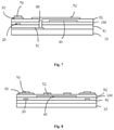
- FIG. 6 is a plan view illustrating a structure of another touch display substrate according to some embodiments the present disclosure
- FIG. 7 is a cross-sectional view taken along line A-A′ of the touch display substrate of FIG. 6
- FIG. 8 is a cross-sectional view taken along line B-B′ of the touch display substrate of FIG. 6 .
- the touch display substrate further includes a plurality of auxiliary conductive lines 70 , and a respective one of the plurality of auxiliary conductive lines 70 is disposed on and electrically connected to a surface of a respective one of the plurality of shielding lines 30 .
- a respective one of the plurality of auxiliary lines 70 is disposed on and in direct contact with a surface of a respective one of the plurality of shielding lines 30 .
- the auxiliary conductive line 70 is formed of a conductive material, which corresponds to a conductive line connected in parallel to the shielding line 30 , and thus the resistance can be reduced, which facilitates the transmission of signals therein.
- FIG. 9 is a plan view illustrating a structure of another touch display substrate according to some embodiments of the present disclosure.
- the touch display substrate further includes a plurality of gate lines 80 insulated from and crossing the plurality of shielding lines 30 .
- a respective one of the plurality of shielding lines 30 (and optionally an auxiliary conductive line 70 thereon) has a spacing at an overlap of an orthographic projection of a respective one of the plurality of gate lines 80 on the base substrate 10 and an orthographic projection of a respective one of the plurality of data lines 20 on the base substrate 10 . That is, as shown in FIG.
- a respective one of the plurality of shielding lines 30 may include a plurality of shielding line segments, and adjacent ones of the plurality of shielding line segments (and optionally an auxiliary conductive line thereon) have a spacing therebetween at an overlap of an orthographic projection of a respective one of the plurality of gate lines 80 on the base substrate 10 and an orthographic projection of a respective one of the plurality of data lines 20 on the base substrate 10 .
- the plurality of shielding line segments are electrically connected together for transmitting a signal.
- the embodiment shown in FIG. 9 may further reduce the coupling capacitance between the shielding line 30 and the data line 20 , thereby reducing the effect on the signal in the data line 20 .
- suitable conductive-line materials may be used for making the gate line 80 , the data line 20 , the common electrode line 51 , and the shielding line 30 .
- suitable conductive-line materials for making the gate line 80 , the data line 20 , the common electrode line 51 , and the shielding line 30 may include, but are not limited to, metal materials such as Cu, Al, Mo, Ti, Cr, and W, and alloys thereof.
- the gate line 80 , the data line 20 , the common electrode line 51 , or the shielding line 30 may have a single-layer structure or a multi-layer structure, such as Mo ⁇ Al ⁇ Mo, Ti ⁇ Cu ⁇ Ti, or Mo ⁇ Ti ⁇ Cu.
- suitable insulating materials may be used for making the gate insulating layer 91 .
- suitable insulating materials for making the gate insulating layer 91 may include, but are not limited to, silicon nitride or silicon oxide.
- the gate insulating layer 91 may have a single-layer structure or a multi-layer structure, for example, a double-layer structure of silicon oxide/silicon nitride.
- suitable passivation materials may be used for making the passivation layer 100 .
- suitable passivation materials for making the passivation layer 100 may include, but are not limited to, silicon nitride or silicon oxide.
- the passivation layer 100 may have a single-layer structure or a multi-layer structure, such as a structure of silicon oxide/silicon nitride.
- suitable insulating materials may be used for making the first insulating layer 92 .
- suitable insulating materials for making the first insulating layer 92 may include, but are not limited to, silicon nitride or silicon oxide.
- the first insulating layer 92 may have a single-layer structure or a multi-layer structure, such as a structure of silicon oxide/silicon nitride.
- suitable electrode materials may be used for making the pixel electrode 40 .
- suitable electrode materials for making the pixel electrode 40 may include, but are not limited to, ITO, IZO, or other transparent metal oxide conductive materials.
- suitable conductive materials may be used for making the common electrode block 52 and the integral common electrode strip 50 .
- suitable conductive materials for making the common electrode block 52 and the integral common electrode strip 50 may include, but are not limited to, ITO, IZO or other transparent metal oxide conductive materials.
- the shielding line 30 may be made of the same material as the common electrode block and the common electrode strip.
- an embodiment of the present disclosure further provides a touch display method, which can be applied to any touch display substrate described herein, and the method includes: outputting a common voltage level to the common electrode and the plurality of shielding lines 30 in a display stage; and sequentially providing a touch driving signal to each of the first touch electrodes and receiving a touch sensing signal from each of the second touch electrodes in the touch stage, or sequentially providing a touch driving signal to each of the second touch electrodes and receiving a touch sensing signal from each of the first touch electrodes in the touch stage.
- FIG. 4 is a schematic diagram of touch and display of the touch display substrate of FIG. 1 .
- a respective one of the plurality of common electrode lines 51 is connected with a liquid crystal driving circuit through a respective one of a plurality of first switches Si to receive a common voltage level Vcom, so as to apply the common voltage level Vcom to the common electrode blocks 52 electrically connected to the respective one of the plurality of common electrode lines 51
- a respective one of the shielding lines 30 is connected with the liquid crystal driving circuit through a respective one of a plurality of second switches S 2 to receive the common voltage level Vcom, so as to apply the common voltage level Vcom to the respective one of the shielding lines 30 .
- the plurality of common electrode lines 51 are connected with a touch detection circuit through the plurality of first switches Si to receive the touch driving signal Tx, so as to apply the touch driving signal Tx to each common electrode block 52
- the plurality of shielding lines 30 are connected with the touch detection circuit through the plurality of second switches S 2 to output the touch sensing signal Rx, so that the touch detection circuit can detect the touch sensing signal Rx in each shielding line 30 .
- the common electrode block 52 may also be used for outputting the touch sensing signal Rx to the touch detection circuit, and the shielding line 30 may also be used for receiving the touch driving signal Tx from the touch detection circuit.
- the present disclosure is not limited thereto.
- the liquid crystal driving circuit and the touch detection circuit may be devices with signal sending capability, such as a voltage source, a chip and the like, and may be mutually independent or integrated.
- mutual-capacitance touch can be realized by only changing the shapes and the connection relationship of the common electrode and the shielding line without adding a new electrode structure on the basis of the conventional liquid crystal touch display substrate.
- an embodiment of the present disclosure further provides a touch display device, which includes any one of the touch display substrates described herein.
- the touch display device may be any product or component having a display function, such as a liquid crystal touch display panel, a liquid crystal touch display module, a mobile phone, a tablet computer, a television, a display, a notebook computer, a digital photo frame, a navigator and the like.
- the touch display device further includes a liquid crystal driving circuit and a touch detection circuit.
- the liquid crystal driving circuit is configured to output a common voltage level to the common electrode and the shielding lines in a display stage; and the touch detection circuit is configured to provide a touch driving signal to each of the first touch electrodes sequentially and receive a touch sensing signal from each of the second touch electrodes in a touch stage, or provide a touch driving signal to each of the second touch electrodes sequentially and receive a touch sensing signal from each of the first touch electrodes in a touch stage.
- the liquid crystal driving circuit and the touch detection circuit are configured to implement the two functions of liquid crystal display and mutual-capacitance touch in a time-sharing manner.
Landscapes
- Engineering & Computer Science (AREA)
- Physics & Mathematics (AREA)
- General Engineering & Computer Science (AREA)
- Theoretical Computer Science (AREA)
- General Physics & Mathematics (AREA)
- Nonlinear Science (AREA)
- Human Computer Interaction (AREA)
- Crystallography & Structural Chemistry (AREA)
- Chemical & Material Sciences (AREA)
- Mathematical Physics (AREA)
- Optics & Photonics (AREA)
- Geometry (AREA)
- Computer Networks & Wireless Communication (AREA)
- Microelectronics & Electronic Packaging (AREA)
- Liquid Crystal (AREA)
- Devices For Indicating Variable Information By Combining Individual Elements (AREA)
- Position Input By Displaying (AREA)
Abstract
Description
Claims (20)
Applications Claiming Priority (3)
| Application Number | Priority Date | Filing Date | Title |
|---|---|---|---|
| CN201810468133.XA CN108762550B (en) | 2018-05-16 | 2018-05-16 | Touch display substrate, touch display method and touch display device |
| CN201810468133.X | 2018-05-16 | ||
| PCT/CN2019/081727 WO2019218800A1 (en) | 2018-05-16 | 2019-04-08 | Touch display substrate, touch display method and touch display device |
Publications (2)
| Publication Number | Publication Date |
|---|---|
| US20210333910A1 US20210333910A1 (en) | 2021-10-28 |
| US11226694B2 true US11226694B2 (en) | 2022-01-18 |
Family
ID=64008182
Family Applications (1)
| Application Number | Title | Priority Date | Filing Date |
|---|---|---|---|
| US16/610,239 Expired - Fee Related US11226694B2 (en) | 2018-05-16 | 2019-04-08 | Touch display substrate, touch display method and touch display device |
Country Status (3)
| Country | Link |
|---|---|
| US (1) | US11226694B2 (en) |
| CN (1) | CN108762550B (en) |
| WO (1) | WO2019218800A1 (en) |
Families Citing this family (4)
| Publication number | Priority date | Publication date | Assignee | Title |
|---|---|---|---|---|
| CN108762550B (en) * | 2018-05-16 | 2021-01-15 | 京东方科技集团股份有限公司 | Touch display substrate, touch display method and touch display device |
| CN113760114B (en) * | 2020-06-03 | 2024-03-01 | 京东方科技集团股份有限公司 | Touch panel, driving method and display device thereof |
| TWI766551B (en) * | 2021-01-20 | 2022-06-01 | 速博思股份有限公司 | Fingerprint-touch sensing apparatus |
| CN113835560B (en) * | 2021-09-27 | 2023-09-08 | 武汉华星光电半导体显示技术有限公司 | Touch display panel and display device |
Citations (12)
| Publication number | Priority date | Publication date | Assignee | Title |
|---|---|---|---|---|
| WO2012118513A1 (en) | 2011-03-03 | 2012-09-07 | Apple Inc. | Display screen shield line system |
| CN103677475A (en) | 2013-12-06 | 2014-03-26 | 京东方科技集团股份有限公司 | Embedded touch display panel and touch positioning method and display device thereof |
| CN104238222A (en) | 2014-10-14 | 2014-12-24 | 上海天马微电子有限公司 | Touch display device and touch display substrate |
| CN104536633A (en) | 2015-01-26 | 2015-04-22 | 京东方科技集团股份有限公司 | Array substrate, manufacturing method thereof and display device |
| CN104808885A (en) | 2015-05-11 | 2015-07-29 | 武汉华星光电技术有限公司 | Array substrate and touch display device |
| CN204883646U (en) | 2015-08-07 | 2015-12-16 | 宸鸿光电科技股份有限公司 | touch panel |
| CN106324924A (en) | 2016-10-21 | 2017-01-11 | 京东方科技集团股份有限公司 | Array substrate, preparation method thereof, display panel and display device |
| CN107065365A (en) | 2017-06-16 | 2017-08-18 | 厦门天马微电子有限公司 | Display panel and display device |
| US20170277329A1 (en) * | 2015-10-22 | 2017-09-28 | Boe Technology Group Co., Ltd. | Touch Screen and Driving Method Thereof, and Display Apparatus |
| CN206931072U (en) | 2017-07-03 | 2018-01-26 | 合肥鑫晟光电科技有限公司 | Electronic equipment, touch control display apparatus and contact panel |
| CN108762550A (en) | 2018-05-16 | 2018-11-06 | 京东方科技集团股份有限公司 | Touch display substrate, touch control display method and touch control display apparatus |
| US20190354212A1 (en) * | 2018-05-15 | 2019-11-21 | E Ink Holdings Inc. | Touch sensor, electronic paper display panel and electronic paper display apparatus |
-
2018
- 2018-05-16 CN CN201810468133.XA patent/CN108762550B/en not_active Expired - Fee Related
-
2019
- 2019-04-08 WO PCT/CN2019/081727 patent/WO2019218800A1/en not_active Ceased
- 2019-04-08 US US16/610,239 patent/US11226694B2/en not_active Expired - Fee Related
Patent Citations (15)
| Publication number | Priority date | Publication date | Assignee | Title |
|---|---|---|---|---|
| WO2012118513A1 (en) | 2011-03-03 | 2012-09-07 | Apple Inc. | Display screen shield line system |
| CN103677475A (en) | 2013-12-06 | 2014-03-26 | 京东方科技集团股份有限公司 | Embedded touch display panel and touch positioning method and display device thereof |
| CN104238222A (en) | 2014-10-14 | 2014-12-24 | 上海天马微电子有限公司 | Touch display device and touch display substrate |
| US20160216817A1 (en) | 2015-01-26 | 2016-07-28 | Boe Technology Group Co., Ltd. | Array substrate, method for producing the same and display apparatus |
| CN104536633A (en) | 2015-01-26 | 2015-04-22 | 京东方科技集团股份有限公司 | Array substrate, manufacturing method thereof and display device |
| CN104808885A (en) | 2015-05-11 | 2015-07-29 | 武汉华星光电技术有限公司 | Array substrate and touch display device |
| US20180113541A1 (en) | 2015-05-11 | 2018-04-26 | Wuhan China Star Optoelectronics Technology Co., Ltd. | Array substrate and touch display device |
| CN204883646U (en) | 2015-08-07 | 2015-12-16 | 宸鸿光电科技股份有限公司 | touch panel |
| US20170277329A1 (en) * | 2015-10-22 | 2017-09-28 | Boe Technology Group Co., Ltd. | Touch Screen and Driving Method Thereof, and Display Apparatus |
| CN106324924A (en) | 2016-10-21 | 2017-01-11 | 京东方科技集团股份有限公司 | Array substrate, preparation method thereof, display panel and display device |
| US20180299984A1 (en) | 2016-10-21 | 2018-10-18 | Boe Technology Group Co., Ltd. | Array substrate, method of fabricating array substrate, display panel, and display device |
| CN107065365A (en) | 2017-06-16 | 2017-08-18 | 厦门天马微电子有限公司 | Display panel and display device |
| CN206931072U (en) | 2017-07-03 | 2018-01-26 | 合肥鑫晟光电科技有限公司 | Electronic equipment, touch control display apparatus and contact panel |
| US20190354212A1 (en) * | 2018-05-15 | 2019-11-21 | E Ink Holdings Inc. | Touch sensor, electronic paper display panel and electronic paper display apparatus |
| CN108762550A (en) | 2018-05-16 | 2018-11-06 | 京东方科技集团股份有限公司 | Touch display substrate, touch control display method and touch control display apparatus |
Non-Patent Citations (2)
| Title |
|---|
| Office Action dated Nov. 25, 2019 issued in corresponding Chinese Application No. 201810468133.X. |
| Second Office Action dated May 15, 2020 corresponding to Chinese application No. 201810468133.X. |
Also Published As
| Publication number | Publication date |
|---|---|
| WO2019218800A1 (en) | 2019-11-21 |
| CN108762550A (en) | 2018-11-06 |
| CN108762550B (en) | 2021-01-15 |
| US20210333910A1 (en) | 2021-10-28 |
Similar Documents
| Publication | Publication Date | Title |
|---|---|---|
| US10572044B2 (en) | Touch-type display panel and short-repair method thereof | |
| KR102468767B1 (en) | Touch-Integrated Display Panel for Display Device | |
| US10268304B2 (en) | Touch display panel, manufacturing method for the same, driving method for the same, and display device | |
| KR102579368B1 (en) | Display panel with external signal lines under gate drive circuit | |
| KR102461365B1 (en) | Touch display panel and touch display device | |
| KR102463812B1 (en) | Touch display device and touch sensing method | |
| KR102463801B1 (en) | Touch display device and touch sensing method | |
| US10585515B2 (en) | Display device with position inputting function | |
| US10698545B2 (en) | Display device with position input function | |
| US11226694B2 (en) | Touch display substrate, touch display method and touch display device | |
| CN104951143B (en) | Array substrate, touch panel and display device | |
| US10712852B2 (en) | Display device with position inputting function | |
| KR102579383B1 (en) | Touch recognition enabled display panel with asymmetric black matrix pattern | |
| EP3662355B1 (en) | Touch control array substrate and touch control display apparatus | |
| TW201504868A (en) | In-cell touch display panel | |
| US20180181239A1 (en) | Liquid crystal display device with touch sensor and method for driving the same | |
| US10042494B2 (en) | Array substrate, touch display panel and touch display device | |
| US10019090B2 (en) | Display with touch sensor circuitry | |
| KR20150067564A (en) | Display Panel For Display Device | |
| KR20170076187A (en) | In-cell touch type display device | |
| CN111708237B (en) | Array substrate, display panel and display device | |
| WO2016084728A1 (en) | Position input device and display device fitted with position input function | |
| KR20210084838A (en) | Display device | |
| US10459298B2 (en) | Display device, array substrate and manufacturing method thereof | |
| JP2019086575A (en) | Display device |
Legal Events
| Date | Code | Title | Description |
|---|---|---|---|
| FEPP | Fee payment procedure |
Free format text: ENTITY STATUS SET TO UNDISCOUNTED (ORIGINAL EVENT CODE: BIG.); ENTITY STATUS OF PATENT OWNER: LARGE ENTITY |
|
| AS | Assignment |
Owner name: BOE TECHNOLOGY GROUP CO., LTD., CHINA Free format text: ASSIGNMENT OF ASSIGNORS INTEREST;ASSIGNOR:CHENG, HONGFEI;REEL/FRAME:050914/0710 Effective date: 20190805 |
|
| STPP | Information on status: patent application and granting procedure in general |
Free format text: NOTICE OF ALLOWANCE MAILED -- APPLICATION RECEIVED IN OFFICE OF PUBLICATIONS |
|
| STPP | Information on status: patent application and granting procedure in general |
Free format text: PUBLICATIONS -- ISSUE FEE PAYMENT VERIFIED |
|
| STCF | Information on status: patent grant |
Free format text: PATENTED CASE |
|
| FEPP | Fee payment procedure |
Free format text: MAINTENANCE FEE REMINDER MAILED (ORIGINAL EVENT CODE: REM.); ENTITY STATUS OF PATENT OWNER: LARGE ENTITY |
|
| LAPS | Lapse for failure to pay maintenance fees |
Free format text: PATENT EXPIRED FOR FAILURE TO PAY MAINTENANCE FEES (ORIGINAL EVENT CODE: EXP.); ENTITY STATUS OF PATENT OWNER: LARGE ENTITY |
|
| STCH | Information on status: patent discontinuation |
Free format text: PATENT EXPIRED DUE TO NONPAYMENT OF MAINTENANCE FEES UNDER 37 CFR 1.362 |
|
| FP | Lapsed due to failure to pay maintenance fee |
Effective date: 20260118 |