US11226530B2 - Active matrix substrate and method for manufacturing active matrix substrate - Google Patents
Active matrix substrate and method for manufacturing active matrix substrate Download PDFInfo
- Publication number
- US11226530B2 US11226530B2 US17/125,174 US202017125174A US11226530B2 US 11226530 B2 US11226530 B2 US 11226530B2 US 202017125174 A US202017125174 A US 202017125174A US 11226530 B2 US11226530 B2 US 11226530B2
- Authority
- US
- United States
- Prior art keywords
- layer
- source
- film
- semiconductor
- gate insulating
- Prior art date
- Legal status (The legal status is an assumption and is not a legal conclusion. Google has not performed a legal analysis and makes no representation as to the accuracy of the status listed.)
- Expired - Fee Related
Links
Images


Classifications
-
- G—PHYSICS
- G02—OPTICS
- G02F—OPTICAL DEVICES OR ARRANGEMENTS FOR THE CONTROL OF LIGHT BY MODIFICATION OF THE OPTICAL PROPERTIES OF THE MEDIA OF THE ELEMENTS INVOLVED THEREIN; NON-LINEAR OPTICS; FREQUENCY-CHANGING OF LIGHT; OPTICAL LOGIC ELEMENTS; OPTICAL ANALOGUE/DIGITAL CONVERTERS
- G02F1/00—Devices or arrangements for the control of the intensity, colour, phase, polarisation or direction of light arriving from an independent light source, e.g. switching, gating or modulating; Non-linear optics
- G02F1/01—Devices or arrangements for the control of the intensity, colour, phase, polarisation or direction of light arriving from an independent light source, e.g. switching, gating or modulating; Non-linear optics for the control of the intensity, phase, polarisation or colour
- G02F1/13—Devices or arrangements for the control of the intensity, colour, phase, polarisation or direction of light arriving from an independent light source, e.g. switching, gating or modulating; Non-linear optics for the control of the intensity, phase, polarisation or colour based on liquid crystals, e.g. single liquid crystal display cells
- G02F1/133—Constructional arrangements; Operation of liquid crystal cells; Circuit arrangements
- G02F1/136—Liquid crystal cells structurally associated with a semi-conducting layer or substrate, e.g. cells forming part of an integrated circuit
- G02F1/1362—Active matrix addressed cells
- G02F1/136286—Wiring, e.g. gate line, drain line
-
- G—PHYSICS
- G02—OPTICS
- G02F—OPTICAL DEVICES OR ARRANGEMENTS FOR THE CONTROL OF LIGHT BY MODIFICATION OF THE OPTICAL PROPERTIES OF THE MEDIA OF THE ELEMENTS INVOLVED THEREIN; NON-LINEAR OPTICS; FREQUENCY-CHANGING OF LIGHT; OPTICAL LOGIC ELEMENTS; OPTICAL ANALOGUE/DIGITAL CONVERTERS
- G02F1/00—Devices or arrangements for the control of the intensity, colour, phase, polarisation or direction of light arriving from an independent light source, e.g. switching, gating or modulating; Non-linear optics
- G02F1/01—Devices or arrangements for the control of the intensity, colour, phase, polarisation or direction of light arriving from an independent light source, e.g. switching, gating or modulating; Non-linear optics for the control of the intensity, phase, polarisation or colour
- G02F1/13—Devices or arrangements for the control of the intensity, colour, phase, polarisation or direction of light arriving from an independent light source, e.g. switching, gating or modulating; Non-linear optics for the control of the intensity, phase, polarisation or colour based on liquid crystals, e.g. single liquid crystal display cells
- G02F1/133—Constructional arrangements; Operation of liquid crystal cells; Circuit arrangements
- G02F1/1333—Constructional arrangements; Manufacturing methods
- G02F1/1343—Electrodes
- G02F1/134309—Electrodes characterised by their geometrical arrangement
- G02F1/134372—Electrodes characterised by their geometrical arrangement for fringe field switching [FFS] where the common electrode is not patterned
-
- G—PHYSICS
- G02—OPTICS
- G02F—OPTICAL DEVICES OR ARRANGEMENTS FOR THE CONTROL OF LIGHT BY MODIFICATION OF THE OPTICAL PROPERTIES OF THE MEDIA OF THE ELEMENTS INVOLVED THEREIN; NON-LINEAR OPTICS; FREQUENCY-CHANGING OF LIGHT; OPTICAL LOGIC ELEMENTS; OPTICAL ANALOGUE/DIGITAL CONVERTERS
- G02F1/00—Devices or arrangements for the control of the intensity, colour, phase, polarisation or direction of light arriving from an independent light source, e.g. switching, gating or modulating; Non-linear optics
- G02F1/01—Devices or arrangements for the control of the intensity, colour, phase, polarisation or direction of light arriving from an independent light source, e.g. switching, gating or modulating; Non-linear optics for the control of the intensity, phase, polarisation or colour
- G02F1/13—Devices or arrangements for the control of the intensity, colour, phase, polarisation or direction of light arriving from an independent light source, e.g. switching, gating or modulating; Non-linear optics for the control of the intensity, phase, polarisation or colour based on liquid crystals, e.g. single liquid crystal display cells
- G02F1/133—Constructional arrangements; Operation of liquid crystal cells; Circuit arrangements
- G02F1/136—Liquid crystal cells structurally associated with a semi-conducting layer or substrate, e.g. cells forming part of an integrated circuit
- G02F1/1362—Active matrix addressed cells
- G02F1/1368—Active matrix addressed cells in which the switching element is a three-electrode device
-
- H01L27/124—
-
- H01L27/1248—
-
- H01L27/127—
-
- H01L27/1288—
-
- H—ELECTRICITY
- H10—SEMICONDUCTOR DEVICES; ELECTRIC SOLID-STATE DEVICES NOT OTHERWISE PROVIDED FOR
- H10D—INORGANIC ELECTRIC SEMICONDUCTOR DEVICES
- H10D86/00—Integrated devices formed in or on insulating or conducting substrates, e.g. formed in silicon-on-insulator [SOI] substrates or on stainless steel or glass substrates
- H10D86/01—Manufacture or treatment
- H10D86/021—Manufacture or treatment of multiple TFTs
- H10D86/0221—Manufacture or treatment of multiple TFTs comprising manufacture, treatment or patterning of TFT semiconductor bodies
-
- H—ELECTRICITY
- H10—SEMICONDUCTOR DEVICES; ELECTRIC SOLID-STATE DEVICES NOT OTHERWISE PROVIDED FOR
- H10D—INORGANIC ELECTRIC SEMICONDUCTOR DEVICES
- H10D86/00—Integrated devices formed in or on insulating or conducting substrates, e.g. formed in silicon-on-insulator [SOI] substrates or on stainless steel or glass substrates
- H10D86/01—Manufacture or treatment
- H10D86/021—Manufacture or treatment of multiple TFTs
- H10D86/0231—Manufacture or treatment of multiple TFTs using masks, e.g. half-tone masks
-
- H—ELECTRICITY
- H10—SEMICONDUCTOR DEVICES; ELECTRIC SOLID-STATE DEVICES NOT OTHERWISE PROVIDED FOR
- H10D—INORGANIC ELECTRIC SEMICONDUCTOR DEVICES
- H10D86/00—Integrated devices formed in or on insulating or conducting substrates, e.g. formed in silicon-on-insulator [SOI] substrates or on stainless steel or glass substrates
- H10D86/40—Integrated devices formed in or on insulating or conducting substrates, e.g. formed in silicon-on-insulator [SOI] substrates or on stainless steel or glass substrates characterised by multiple TFTs
- H10D86/441—Interconnections, e.g. scanning lines
-
- H—ELECTRICITY
- H10—SEMICONDUCTOR DEVICES; ELECTRIC SOLID-STATE DEVICES NOT OTHERWISE PROVIDED FOR
- H10D—INORGANIC ELECTRIC SEMICONDUCTOR DEVICES
- H10D86/00—Integrated devices formed in or on insulating or conducting substrates, e.g. formed in silicon-on-insulator [SOI] substrates or on stainless steel or glass substrates
- H10D86/40—Integrated devices formed in or on insulating or conducting substrates, e.g. formed in silicon-on-insulator [SOI] substrates or on stainless steel or glass substrates characterised by multiple TFTs
- H10D86/451—Integrated devices formed in or on insulating or conducting substrates, e.g. formed in silicon-on-insulator [SOI] substrates or on stainless steel or glass substrates characterised by multiple TFTs characterised by the compositions or shapes of the interlayer dielectrics
-
- H—ELECTRICITY
- H10—SEMICONDUCTOR DEVICES; ELECTRIC SOLID-STATE DEVICES NOT OTHERWISE PROVIDED FOR
- H10D—INORGANIC ELECTRIC SEMICONDUCTOR DEVICES
- H10D86/00—Integrated devices formed in or on insulating or conducting substrates, e.g. formed in silicon-on-insulator [SOI] substrates or on stainless steel or glass substrates
- H10D86/40—Integrated devices formed in or on insulating or conducting substrates, e.g. formed in silicon-on-insulator [SOI] substrates or on stainless steel or glass substrates characterised by multiple TFTs
- H10D86/60—Integrated devices formed in or on insulating or conducting substrates, e.g. formed in silicon-on-insulator [SOI] substrates or on stainless steel or glass substrates characterised by multiple TFTs wherein the TFTs are in active matrices
-
- G—PHYSICS
- G02—OPTICS
- G02F—OPTICAL DEVICES OR ARRANGEMENTS FOR THE CONTROL OF LIGHT BY MODIFICATION OF THE OPTICAL PROPERTIES OF THE MEDIA OF THE ELEMENTS INVOLVED THEREIN; NON-LINEAR OPTICS; FREQUENCY-CHANGING OF LIGHT; OPTICAL LOGIC ELEMENTS; OPTICAL ANALOGUE/DIGITAL CONVERTERS
- G02F2201/00—Constructional arrangements not provided for in groups G02F1/00 - G02F7/00
- G02F2201/12—Constructional arrangements not provided for in groups G02F1/00 - G02F7/00 electrode
- G02F2201/121—Constructional arrangements not provided for in groups G02F1/00 - G02F7/00 electrode common or background
-
- G—PHYSICS
- G02—OPTICS
- G02F—OPTICAL DEVICES OR ARRANGEMENTS FOR THE CONTROL OF LIGHT BY MODIFICATION OF THE OPTICAL PROPERTIES OF THE MEDIA OF THE ELEMENTS INVOLVED THEREIN; NON-LINEAR OPTICS; FREQUENCY-CHANGING OF LIGHT; OPTICAL LOGIC ELEMENTS; OPTICAL ANALOGUE/DIGITAL CONVERTERS
- G02F2201/00—Constructional arrangements not provided for in groups G02F1/00 - G02F7/00
- G02F2201/12—Constructional arrangements not provided for in groups G02F1/00 - G02F7/00 electrode
- G02F2201/123—Constructional arrangements not provided for in groups G02F1/00 - G02F7/00 electrode pixel
Definitions
- the present invention relates to an active matrix substrate and a method for manufacturing an active matrix substrate.
- an active matrix liquid crystal display device includes a substrate (hereinafter called “active matrix substrate”) having a thin-film transistor (hereinafter also called “TFT”) formed as a switching element for each pixel, a counter substrate having formed therein a counter electrode, a color filter, and the like, a liquid crystal layer provided between the active matrix substrate and the counter substrate, and a pair of electrodes (namely an pixel electrode and a common electrode) through which to apply a voltage to the liquid crystal layer.
- pixel TFT a thin-film transistor provided as a switching element for each pixel of the active matrix substrate.
- operation modes have been proposed for and adopted into active matrix liquid crystal display devices according to the purposes for which the devices are used.
- Known examples of operation modes include transverse electric field modes such as an IPS (in-plane switching) mode and an FFS (fringe field switching) mode.
- IPS in-plane switching
- FFS far field switching
- an active matrix substrate is provided with a pixel electrode and a common electrode, and an electric field is applied to liquid crystal molecules in a direction (transverse direction) parallel to a board surface.
- a pixel electrode and a common electrode are disposed so as to overlap each other via an insulating film (dielectric layer), so that a higher aperture ratio and a higher transmittance can be achieved than in a liquid crystal display device of the IPS mode.
- a capacitance is formed in a place where the pixel electrode and the common electrode overlap each other via the dielectric layer. This capacitance may have a function as an auxiliary capacitance (hereinafter called “transparent auxiliary capacitance”) in the display device.
- PTL 1 discloses an active matrix substrate that is used in the FFS mode.
- a source bus line and source and drain electrodes of a pixel TFT each have a laminated structure including a lower layer composed of a metal film (called “source conducting film”) and an upper layer composed of a transparent conducting film for use in a pixel electrode.
- source conducting film a metal film
- transparent conducting film a transparent conducting film for use in a pixel electrode.
- a resist mask that is used in patterning of the source conducting film is utilized to perform patterning of a semiconductor film that serves as an active layer of the pixel TFT and a contact film that serves as a contact layer of the pixel TFT.
- a resist mask that is used in patterning of the transparent conducting film is utilized to perform etching by which the source conducting film and the contact film are separated into a source side and a drain side, so that a portion of the active layer that serves as a channel is exposed. This makes it possible to reduce the number of photomasks that are used (i.e. the number of photolithography steps).
- a conventional process for manufacturing an active matrix substrate may reduce yields due to leak defects, display defects, and the like that are described below.
- a part of the dielectric layer located between the pixel electrode and the common electrode is disposed so as to make direct contact with a gate insulating layer that has a comparatively high film stress. For this reason, when the dielectric layer is thin, there is a risk that adhesion with the gate insulating layer may decrease. Meanwhile, when the dielectric layer is made thicker for securement of sufficient adhesion with the gate insulating layer, the aforementioned transparent auxiliary capacitance becomes smaller, so that there is a possibility that a shadowing or flicker display defect may tend to occur.
- the conventional manufacturing process poses a risk that a part of the contact film may be altered to form a silicon product that remains as a residue on the active layer of the pixel TFT. This may be a factor in the occurrence of a source-drain leak.
- An embodiment of the present invention has as an object to provide an active matrix substrate that is capable of improving yields by reducing defects such as leak defects and display defects such as those described above and a method for manufacturing such an active matrix substrate.
- an active matrix substrate and a method for manufacturing an active matrix substrate according to the following items.
- each of the plurality of pixel regions has
- the source electrode and the drain electrode of the thin-film transistor each have a laminated structure including a lower layer formed from a source conducting film and an upper layer formed from a first transparent conducting film,
- the pixel electrode is formed from the first transparent conducting film
- the gate insulating layer includes a first region including a portion of the thin-film transistor that makes contact with the semiconductor layer and a first thinned region that is thinner than the first region,
- the pixel electrode is disposed over a part of the first thinned region
- the dielectric layer is in direct contact with another part of the first thinned region
- an upper surface of the gate insulating layer has a stepped portion that serves as a boundary between the first region and the first thinned region
- the stepped portion when seen from a direction of a normal to the substrate, includes a first stepped portion that extends flush with a side surface of the lower layer of the drain electrode, and
- the pixel electrode extends over at least a part of the first stepped portion and at least a part of the side surface of the lower layer of the drain electrode from above the first thinned region and is connected to the upper layer of the drain electrode.
- the first thinned region of the gate insulating layer includes a second region and a third region that is thinner than the second region
- the upper surface of the gate insulating layer further has a second stepped portion that serves as a boundary between the second region and the third region,
- the pixel electrode is disposed over the second region
- the dielectric region is in contact with the third region
- the second stepped portion when seen from the direction of the normal to the substrate, at least a part of the second stepped portion is flush with a side surface of the pixel electrode.
- the dielectric layer has a laminated structure including a lower dielectric layer that makes direct contact with the gate insulating layer and an upper dielectric layer disposed over the lower dielectric layer,
- either one of the lower dielectric layer and the upper dielectric layer has a compressive stress
- the other one of the lower dielectric layer and the upper dielectric layer has a tensile stress.
- the gate insulating layer has a compressive stress
- the lower dielectric layer has a compressive stress
- the upper dielectric layer has a tensile stress.
- the plurality of source bus lines each have a laminated structure including a lower line formed from the source conducting film and an upper line formed from the first transparent conducting film,
- the source electrode of each of the pixel regions is electrically connected to one of the plurality of source bus lines, and
- the lower line of the one source bus line is in direct contact with the first region of the gate insulating layer.
- the gate insulating layer in each of the pixel regions, when seen from the direction of the normal to the substrate, the gate insulating layer further has a second thinned region that extends along a peripheral edge of the one source bus line between the third region and the one source bus line,
- the second thinned region is thinner than the first region and thicker than the first thinned region
- the second thinned region is in direct contact with the dielectric layer.
- the semiconductor layer includes a first source semiconductor section extended between the one source bus line and the gate insulating layer,
- the source contact layer includes a second source semiconductor section extended between the one source bus line and the gate insulating layer and located over the first source semiconductor section, and
- the one source bus line covers upper and side surfaces of a laminated body composed of the first source semiconductor section and the second source semiconductor section and is in contact with the gate insulating layer.
- a height h 1 of the first stepped portion is greater than or equal to 100 nm and less than or equal to 150 nm.
- a height h 2 of the second stepped portion is greater than or equal to 20 nm and less than or equal to 40 nm.
- step (h) a step of performing patterning of the first transparent conducting layer and the source conducting layer by wet etching using the second mask, the step causing a first transparent conducting layer to be formed from the first transparent conducting film and a source metal layer to be formed from the source conducting layer, the first transparent conducting layer including an upper layer of a source electrode and an upper layer of a drain electrode of the thin-film transistor, the source metal layer including a lower layer of the source electrode and a lower layer of the drain electrode of the thin-film transistor;
- (k) a step of forming, over the dielectric layer, a second transparent conducting layer including a common electrode.
- the first thinning step is executed under etching conditions where residues of the semiconductor film and the contact semiconductor film left over the gate insulating layer are removable through thicknesses thereof.
- the step (j) includes a step of forming a lower dielectric layer that makes direct contact with the upper surface of the gate insulating layer and a step of forming an upper dielectric layer over the lower dielectric layer, thereby causing the dielectric layer to be formed to have a laminated structure including the lower dielectric layer and the upper dielectric layer,
- either one of the lower dielectric layer and the upper dielectric layer has a compressive stress
- the other one of the lower dielectric layer and the upper dielectric layer has a tensile stress.
- the gate insulating layer has a compressive stress
- the lower dielectric layer has a compressive stress
- the upper dielectric layer has a tensile stress.
- the gate insulating layer is a silicon nitride layer formed at a first temperature Ta
- the lower dielectric layer is a silicon nitride layer formed at a second temperature Tb,
- the upper dielectric layer is a silicon nitride layer formed at a third temperature Tc, and
- the first temperature Ta, the second temperature Tb, and the third temperature Tc satisfy Ta>Tb>Tc.
- An embodiment of the present invention provides an active matrix substrate that is capable of improving yields and a method for manufacturing such an active matrix substrate.
- FIG. 1 is a diagram schematically showing an example of a planar structure of an active matrix substrate 100 of Embodiment 1.
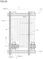
- FIG. 2A is a plan view illustrating each pixel region P in the active matrix substrate 100 .
- FIG. 2B is a cross-sectional view taken along lines IV-IV′ and V-V′ shown in FIG. 2A .
- FIG. 2C is a cross-sectional view taken along line VI-VI′ shown in FIG. 2A .
- FIG. 2D is a cross-sectional view of an etching residue appearance region 104 as taken along line VII-VII′ shown in FIG. 2A .
- FIG. 3A is a step plan view explaining a method for manufacturing an active matrix substrate 100 .
- FIG. 3B is a step plan view explaining the method for manufacturing an active matrix substrate 100 .
- FIG. 3C is a step plan view explaining the method for manufacturing an active matrix substrate 100 .
- FIG. 4A is a step cross-sectional view taken along lines IV-IV′ and V-V′ for explaining the method for manufacturing an active matrix substrate 100 .
- FIG. 4B is a step cross-sectional view taken along lines IV-IV′ and V-V′ for explaining the method for manufacturing an active matrix substrate 100 .
- FIG. 4C is a step cross-sectional view taken along lines IV-IV′ and V-V′ for explaining the method for manufacturing an active matrix substrate 100 .
- FIG. 4D is a step cross-sectional view taken along lines IV-IV′ and V-V′ for explaining the method for manufacturing an active matrix substrate 100 .
- FIG. 4E is a step cross-sectional view taken along lines IV-IV′ and V-V′ for explaining the method for manufacturing an active matrix substrate 100 .
- FIG. 4F is a step cross-sectional view taken along lines IV-IV′ and V-V′ for explaining the method for manufacturing an active matrix substrate 100 .
- FIG. 4G is a step cross-sectional view taken along lines IV-IV′ and V-V′ for explaining the method for manufacturing an active matrix substrate 100 .
- FIG. 5A is a step cross-sectional view taken along line VI-VI′ for explaining the method for manufacturing an active matrix substrate 100 .
- FIG. 5B is a step cross-sectional view taken along line VI-VI′ for explaining the method for manufacturing an active matrix substrate 100 .
- FIG. 5C is a step cross-sectional view taken along line VI-VI′ for explaining the method for manufacturing an active matrix substrate 100 .
- FIG. 5D is a step cross-sectional view taken along line VI-VI′ for explaining the method for manufacturing an active matrix substrate 100 .
- FIG. 5E is a step cross-sectional view taken along line VI-VI′ for explaining the method for manufacturing an active matrix substrate 100 .
- FIG. 5F is a step cross-sectional view taken along line VI-VI′ for explaining the method for manufacturing an active matrix substrate 100 .
- FIG. 5G is a step cross-sectional view taken along line VI-VI′ for explaining the method for manufacturing an active matrix substrate 100 .
- FIG. 6A is a step cross-sectional view of the etching residue appearance region 104 as taken along line VII-VII′ for explaining the method for manufacturing an active matrix substrate 100 .
- FIG. 6B is a step cross-sectional view of the etching residue appearance region 104 as taken along line VII-VII′ for explaining the method for manufacturing an active matrix substrate 100 .
- FIG. 6C is a step cross-sectional view of the etching residue appearance region 104 as taken along line VII-VII′ for explaining the method for manufacturing an active matrix substrate 100 .
- FIG. 6D is a step cross-sectional view of the etching residue appearance region 104 as taken along line VII-VII′ for explaining the method for manufacturing an active matrix substrate 100 .
- FIG. 6E is a step cross-sectional view of the etching residue appearance region 104 as taken along line VII-VII′ for explaining the method for manufacturing an active matrix substrate 100 .
- FIG. 6F is a step cross-sectional view of the etching residue appearance region 104 as taken along line VII-VII′ for explaining the method for manufacturing an active matrix substrate 100 .
- FIG. 6G is a step cross-sectional view of the etching residue appearance region 104 as taken along line VII-VII′ for explaining the method for manufacturing an active matrix substrate 100 .
- FIG. 7 is a diagram schematically showing a process flow of the active matrix substrate 100 .
- FIG. 8 is a diagram illustrating a relationship between the thicknesses and stresses of a lower dielectric layer 11 A and an upper dielectric layer 11 B.
- FIG. 9A is a cross-sectional view of a TFT formation region 101 and a source bus line formation region 102 in an active matrix substrate 200 of a modification.
- FIG. 9B is a cross-sectional view of an etching residue appearance region 104 across a source bus line SL.
- FIG. 10A is a step cross-sectional view taken along lines IV-IV′ and V-V′ for explaining a method for manufacturing an active matrix substrate 200 .
- FIG. 10B is a step cross-sectional view taken along lines IV-IV′ and V-V′ for explaining the method for manufacturing an active matrix substrate 200 .
- FIG. 10C is a step cross-sectional view taken along lines IV-IV′ and V-V′ for explaining the method for manufacturing an active matrix substrate 200 .
- FIG. 10D is a step cross-sectional view taken along lines IV-IV′ and V-V′ for explaining the method for manufacturing an active matrix substrate 200 .
- FIG. 11 is a cross-sectional view showing a TFT formation region 101 and a source bus line formation region 102 in an active matrix substrate 900 of a comparative example.
- FIG. 12A is a step cross-sectional view of the TFT formation region 101 and the source bus line formation region 102 for explaining a method for manufacturing an active matrix substrate 900 of the comparative example.
- FIG. 12B is a step cross-sectional view of the TFT formation region 101 and the source bus line formation region 102 for explaining the method for manufacturing an active matrix substrate 900 of the comparative example.
- FIG. 12C is a step cross-sectional view of the TFT formation region 101 and the source bus line formation region 102 for explaining the method for manufacturing an active matrix substrate 900 of the comparative example.
- FIG. 12D is a step cross-sectional view of the TFT formation region 101 and the source bus line formation region 102 for explaining the method for manufacturing an active matrix substrate 900 of the comparative example.
- FIG. 13A is a step cross-sectional view taken across a TFT 10 in a channel width direction for explaining the method for manufacturing an active matrix substrate 900 of the comparative example.
- FIG. 13B is a step cross-sectional view taken across the TFT 10 in a channel width direction for explaining the method for manufacturing an active matrix substrate 900 of the comparative example.
- FIG. 13C is a step cross-sectional view taken across the TFT 10 in a channel width direction for explaining the method for manufacturing an active matrix substrate 900 of the comparative example.
- FIG. 13D is a step cross-sectional view taken across the TFT 10 in a channel width direction for explaining the method for manufacturing an active matrix substrate 900 of the comparative example.
- FIG. 14A is a step cross-sectional view of the etching residue appearance region 104 for explaining the method for manufacturing an active matrix substrate 900 of the comparative example.
- FIG. 14B is a step cross-sectional view of the etching residue appearance region 104 for explaining the method for manufacturing an active matrix substrate 900 of the comparative example.
- FIG. 14C is a step cross-sectional view of the etching residue appearance region 104 for explaining the method for manufacturing an active matrix substrate 900 of the comparative example.
- FIG. 14D is a step cross-sectional view of the etching residue appearance region 104 for explaining the method for manufacturing an active matrix substrate 900 of the comparative example.
- FIG. 15 schematically shows a process flow of the active matrix substrate 900 of the comparative example.
- FIG. 16 is an enlarged plan view for explaining a wall part 150 formed by a Si product in the active matrix substrate 900 of the comparative example.
- An active matrix substrate of Embodiment 1 is for example an active matrix substrate that is used in a liquid crystal display device of the FFS mode. It should be noted that the active matrix substrate of the present embodiment needs only have a TFT and two transparent conducting layers over a substrate and widely encompasses active matrix substrates that are used in various types of display device and electronic device and the like.
- FIG. 1 is a diagram schematically showing an example of a planar structure of an active matrix substrate 100 of the present embodiment.
- the active matrix substrate 100 has a display region DR that contributes to a display and a peripheral region (frame region) FR located outside the display region DR.
- the display region DR is provided with a plurality of source bus lines SL extending in a first direction (y direction) and a plurality of gate bus lines GL extending in a second direction (x direction) crossing (in this example, orthogonal to) the first direction.
- Each region surrounded by these bus lines serves as a “pixel region P”.
- the pixel region P (sometimes called “pixel”) is a region that corresponds to a pixel of a display device.
- a plurality of the pixel regions P are arranged in a matrix.
- Each pixel region P has formed therein a pixel electrode PE and a thin-film transistor (TFT) 10 .
- Each TFT 10 has its gate electrode electrically connected to a corresponding gate bus line GL and its source electrode electrically connected to a corresponding source bus line SL. Further, each TFT 10 has its drain electrode electrically connected to the pixel electrode PE.
- a common electrode (not illustrated) is provided above the pixel electrode PE via an insulating layer (hereinafter called a “dielectric layer”).
- drive circuits such as a gate driver GD and a source driver SD, an SSD circuit, a plurality of terminal areas, a plurality of source-gate connections, and the like are disposed.
- the gate driver GD and the source driver SD may be monolithically formed or mounted in the active matrix substrate 100 .
- each pixel region P in the active matrix substrate 100 of the present embodiment is more specifically described with reference to the drawings.
- the active matrix substrate 100 has a plurality of the pixel regions P, the following describes a single pixel region P.
- FIG. 2A is a plan view illustrating each pixel region P in the active matrix substrate 100 .
- FIG. 2B is a cross-sectional view taken along line VI-VI′ across the TFT 10 in a channel length direction in a region (TFT formation region) 101 where the TFT 10 is formed and line V-V′ across the source bus line SL in a region (source bus line formation region) 102 where the source bus line SL is formed.
- FIG. 2C is a cross-sectional view taken along line VI-VI′ across the TFT 10 in a channel width direction in the TFT formation region 101 .
- FIG. 2D is a cross-sectional view taken along line VII-VII′ across the source bus line SL in a region (etching residue appearance region) 104 where an etching residue has appeared. Illustrated here is a cross-sectional structure that is finally obtained in a case where a residue of a laminated semiconductor film (hereinafter referred to as “semiconductor residual part”) has appeared so as to make a connection between a pixel electrode formation region 103 where the pixel electrode PE is formed and the source bus line formation region 102 .
- semiconductor residual part a residue of a laminated semiconductor film
- the layers in parentheses indicate in which of the layers each constituent element is formed.
- the pixel region P is for example a region surrounded by source bus lines SL and gate bus lines GL extending in a direction crossing the source bus lines SL.
- the pixel region P has a substrate 1 , a pixel TFT (hereinafter simply referred to as “TFT”) 10 supported by the substrate 1 , a pixel electrode PE, and a common electrode CE.
- TFT pixel TFT
- the pixel TFT 10 needs only be associated with the pixel region P, and a part of the pixel TFT 10 may be located in another pixel region.
- the common electrode CE is disposed over the pixel electrode PE via a dielectric layer (also referred to as “interlayer insulating layer”) 11 .
- the TFT 10 is a TFT of a bottom-gate channel-etch structure.
- the TFT 10 includes a gate electrode GE disposed over the substrate 1 , a gate insulating layer 3 covering the gate electrode GE, a semiconductor layer 5 disposed over the gate electrode GE via the gate insulating layer 3 , a source electrode SE electrically connected to the semiconductor layer 5 , and a drain electrode DE electrically connected to the semiconductor layer 5 .
- the gate electrode GE is electrically connected to a corresponding gate bus line GL
- the source electrode SE is electrically connected to a corresponding source bus line SL.
- the drain electrode DE is connected to the pixel electrode PE.
- the gate electrode GE may be formed integrally with the corresponding gate bus line GL
- the source electrode SE may be formed integrally with the corresponding source bus line SL.
- a source contact layer 7 s and a drain contact layer 7 d are disposed.
- the source contact layer 7 s and the drain contact layer 7 d are disposed on both sides, respectively, of a region (channel region) 5 c of the semiconductor layer 5 where a channel is formed.
- the source electrode SE is disposed over the semiconductor layer 5 via the source contact layer 7 s .
- the drain electrode DE is disposed over the semiconductor layer 5 via the drain contact layer 7 d .
- the source electrode SE may be provided so as to make contact with the source contact layer 7 s
- the drain electrode DE may be provided so as to make contact with the drain contact layer 7 d.
- a first portion (including the channel region 5 c ) of the semiconductor layer 5 that is not covered with the source contact layer 7 s or the drain contact layer 7 d may be surface-etched.
- the first portion is thinner in thickness than a second portion of the semiconductor layer 5 covered with the source contact layer 7 s and the drain contact layer 7 d.
- the source contact layer 7 s and the drain contact layer 7 d are formed, for example, from a contact semiconductor film containing an n-type impurity in a higher concentration than the semiconductor layer 5 .
- the semiconductor layer 5 may be an intrinsic amorphous silicon (i-a-Si) layer, and the source contact layer 7 s and the drain contact layer 7 d may be n + amorphous silicon (n + -a-Si) layers.
- the gate electrode GE and the gate bus line GL are formed within the gate metal layer M 1 (using the gate conducting film).
- the gate electrode GE may be a part of the gate bus line GL or may be connected to the gate bus line GL.
- the source electrode SE and the source bus line SL have a laminated structure including a lower layer 8 s formed within the source metal layer M 2 (using the source conducting film) and an upper layer 9 s formed within the first transparent contacting layer T 1 (using the first transparent conducting film).
- the source electrode SE may be a part of the source line SL or may be connected to the source bus line SL.
- the drain electrode DE too has a laminated structure including a lower layer 8 d formed within the source metal layer M 2 and an upper layer 9 d formed within the first transparent conducting layer T 1 .
- the lower layers 8 s and 8 d are herein sometimes collectively referred to as “lower layer 8 ”, and the upper layers 9 s and 9 d are herein sometimes collectively referred to as “upper layer 9 ”.
- the upper layer 9 is in direct contact with an upper surface of the lower layer 8 .
- the lower layer 8 is a conducting layer (e.g. a metal layer) that is lower in resistance than the upper layer 9 , and may function as a main layer of each electrode or wire.
- the lower layer 8 s and upper layer 9 s of the source bus line SL are sometimes called “lower line” and “upper line”, respectively.
- the source electrode SE (or the source bus line SL) extends over a part of a side surface of the source contact layer 7 s and a part of a side surface of the semiconductor layer 5 and is in contact with the gate insulating layer.
- the drain electrode DE extends over a part of a side surface of the drain contact layer 7 d and a part of a side surface of the semiconductor layer 5 and is in contact with the gate insulating layer 3 .
- the pixel electrode PE is formed within the first transparent conducting layer T 1 .
- the pixel electrode PE is electrically separated from a pixel electrode of an adjacent pixel region. Further, when seen from the direction of the normal to the substrate 1 , the pixel electrode PE and the source bus line SL are placed at a spacing (called “gap portion”) 110 from each other. Further, the pixel electrode PE extends from the pixel electrode formation region 103 into the TFT formation region 101 and is connected to (i.e. formed integrally with) the upper layer 9 d of the drain electrode DE. Accordingly, the upper layer 9 d of the drain electrode DE may function as a part of the pixel electrode PE.
- the TFT 10 and the pixel electrode PE are covered with the dielectric layer 11 .
- the dielectric layer 11 is in direct contact with the channel region 5 c of the TFT 10 and the pixel electrode PE. Further, the dielectric layer 11 is in direct contact with a part of an upper surface of the gate insulating layer 3 , i.e. a portion of the upper surface of the gate insulating layer 3 that is not covered with the semiconductor layer 5 , the source metal layer M 2 , or the first transparent conducting layer T 1 .
- the dielectric layer 11 is in direct contact with the gate insulating layer 3 in the gap portion 110 between the source bus line SL and the pixel PE.
- the dielectric layer 11 is for example an inorganic insulating layer (passivation film).
- the dielectric layer 11 is a silicon nitride (SiN x ) layer.
- the dielectric layer 11 may have a laminated structure.
- the dielectric layer 11 has a laminated structure including a lower dielectric layer 11 A and an upper dielectric layer 11 B in this order from the substrate 1 .
- the common electrode CE is formed over the dielectric layer 11 .
- the common electrode CE is formed within the second transparent conducting layer T 2 (using the second transparent conducting film).
- the common electrode CE is provided with one or more slits (openings) 15 s or notches for each pixel region P. Further, the common electrode CE may have an opening 15 p in the TFT formation region 101 .
- the common electrode CE may be formed all over the pixel region P excluding the TFT formation region 101 . The common electrode CE does not need to be separated for each pixel region P.
- the pixel electrode PE and the common electrode CE are disposed so as to partially overlap each other via the dielectric layer 11 .
- an auxiliary capacitance transparent auxiliary capacitance
- the gate insulating layer 3 includes a first region 31 and a first thinned region 3 t 1 that is thinner than the first region 31 .
- the semiconductor layer 5 (channel region 5 c ) and the source bus line SL are disposed, and over the first thinned region 3 t 1 , the pixel electrode PE is disposed.
- the gate insulating layer 3 is thinned (called “first thinning step”) using a mask (called “source mask” or “first mask”) that is used in patterning of the source conducting film.
- the first thinned region 3 t 1 is a region thinned in the first thinning step.
- the first region 31 is a region kept as thick as it was at the time of formation of the semiconductor film without being etched (thinned) in the first thinning step.
- the first region 31 may be as thick as it was at the time of formation of the gate insulating layer 3 .
- the first region 31 includes, for example, a portion of the gate insulating layer 3 that makes contact with the source bus line SL (or the source electrode SE), a portion of the gate insulating layer 3 that makes contact with the drain electrode DE, a portion of the gate insulating layer 3 that makes contact with the semiconductor layer 5 , and the like.
- the semiconductor layer 5 , the source bus line SL, the source electrode SE, and the drain electrode DE are in contact with the first region 31 of the gate insulating layer 3 but are not in contact with the first thinned region 3 t 1 .
- the first thinned region 3 t 1 is formed mainly in the pixel electrode formation region 103 and the gap portion 110 .
- the first thinned region 3 t 1 includes a portion of the gate insulating layer 3 that makes contact with the dielectric layer 11 , a portion of the gate insulating layer 3 that makes contact with the pixel electrode PE, and the like.
- the upper surface of the gate insulating layer 3 has a first stepped portion (stepped surface) s 1 that serves as a boundary between the first region 31 and the first thinned region 3 t 1 .
- the first stepped portion s 1 is formed by the first thinning step. When seen from the direction of the normal to the substrate 1 , at least a part of the first stepped portion s 1 is located closer to the outside than the semiconductor layer 5 and is flush with a side surface of the lower layer 8 d of the drain electrode DE.
- the pixel electrode PE is extended from above the first thinned region 3 t 1 of the gate insulating layer 3 so as to cover side surfaces of the first stepped portion s 1 and the drain electrode DE and is connected to the upper layer 9 d of the drain electrode DE.
- the first thinned region 3 t 1 of the gate insulating layer 3 may include a second region 32 and a third region 33 that is thinner than the second region 32 .
- a part of the first thinned region 3 t 1 may be further thinned (called “second thinning step”) after the first thinning step using a mask (called “pixel electrode mask” or “second mask”) that is used in patterning of the first transparent conducting film.
- the second region 32 is a region of the first thinned region 3 t 1 that was not thinned in the second thinning step (i.e. that was thinned only in the first thinning step).
- the third region 33 is a region further thinned in the second thinning step (i.e. thinned in both the first and second thinning steps).
- the second region 32 may be disposed in the pixel electrode formation region 103
- the third region 33 may be disposed in the gap portion 110 of the gate insulating layer 3 between the source bus line SL and the pixel electrode PE.
- the pixel electrode PE is disposed over the second region 32 .
- the dielectric layer 11 is in direct contact with the third region 33 in the gap portion 110 .
- An upper surface of the first thinned region 3 t 1 of the gate insulating layer 3 may have a second stepped portion s 2 serving as a boundary between the second region 32 and the third region 33 .
- the second stepped portion s 2 is formed in the second thinning step. When seen from the direction of the normal to the substrate 1 , at least a part of the second stepped portion s 2 may be flush with a side surface of the pixel electrode PE.
- the gate insulating layer 3 may further has a second thinned region 3 t 2 that is thinner than the first region 31 and thicker than the first thinned region 3 t 1 .
- the second thinned region 3 t 2 is a region thinned only in the second thinning step without being thinned in the first thinning step.
- the second thinned region 3 t 2 is formed along a peripheral edge of the source bus lines SL.
- the second thinned region 3 t 2 is located, for example, between the source bus line SL and the third region 33 .
- the upper surface of the gate insulating layer 3 further has a third stepped portion s 3 that serves as a boundary between the first region 31 and the second thinned region 3 t 2 and a fourth stepped portion s 4 that serves as a boundary between the third region 33 and the second thinned region 3 t 2 .
- the first thinning step may be executed under etching conditions where a semiconductor residual part having appeared over the gate insulating layer 3 is removable through the thickness of the semiconductor residual part.
- the settings may be configured for etching conditions where the laminated semiconductor film composed of the semiconductor film by which the semiconductor layer 5 is formed and the contact semiconductor film by which the contact layers 7 s and 7 d are formed is removable through the thickness of the laminated semiconductor film.
- the second thinning step may be executed, for example, at the same time as etching by which the contact semiconductor film is separated into the source contact layer 7 s and the drain contact layer 7 d . In this case, the second thinning step is executed under etching conditions where the contact semiconductor film is entirely removed and only a surface portion of the semiconductor film is removed.
- the thickness h 1 of a surface portion of the gate insulating layer 3 that is removed in the first thinning step may be greater than the thickness h 2 of a surface portion of the gate insulating layer 3 that is removed in the second thinning step (i.e. the height of the second stepped portion s 2 ).
- the height of the third stepped portion s 3 is equal to the thickness h 2 , which is removed in the second thinning step.
- the height of the fourth stepped portion s 4 is equal to the thickness h 1 , which is removed in the first thinning step.
- a portion of the gate insulating layer 3 located between the semiconductor layer 5 and the gate electrode GE is kept at a predetermined thickness, while other portions of the gate insulating layer 3 (e.g. a portion of the gate insulating layer 3 that makes contact with the pixel electrode PE) are thinned. This makes it possible to, while securing desired TFT characteristics, reduce a film stress that is produced in the gate insulating layer 3 .
- the gate insulating layer 3 is thinned substantially all over a region (including the pixel electrode formation region 103 ) in each pixel region that contributes to a display. Since a large portion of the gate insulating layer 3 is thinned in each pixel region, the film stress of the gate insulating layer 3 can be effectively reduced. Further, by further thinning the gate insulating layer 3 in the second thinning step, the film stress of the gate insulating layer 3 can be further reduced.
- the first mask is utilized to perform patterning of the source conducting film and execute the first thinning step on the gate insulating layer 3 .
- the first mask is utilized to perform patterning of the source conducting film and execute the first thinning step on the gate insulating layer 3 .
- a portion of the semiconductor residual part located in a region that is not covered with the first mask can be removed through the thickness thereof in the first thinning step. Accordingly, for example, a semiconductor residual part having appeared over the pixel electrode formation region 103 or in the gap portion 110 between the pixel electrode formation region 103 and the source bus line formation region 102 is removed in the first thinning step. This in turn makes it possible to reduce display defects and leak defects that are attributed to semiconductor residual parts.
- the part 171 (called “semiconductor section”) of the semiconductor residual part is located between the source bus line SL and the gate insulating layer 3 and has an island-shaped pattern separated from the semiconductor layer 5 . Further, the semiconductor section 171 is not in contact with the pixel electrode PE. Accordingly, even when the semiconductor section 171 is formed, no leak occurs between the pixel electrode PE and the source bus line SL.
- leak defects attributed to semiconductor residues can be reduced not only in a case where a semiconductor residual part is entirely removed but also in a case where a semiconductor residual part is partially remains below the source metal layer M 2 (e.g. the source bus line SL).
- etching the semiconductor film and the contact semiconductor film (laminated semiconductor film) using the same mask as the source conducting film may cause a Si product to be formed in the shape of a wall at an edge of the semiconductor layer 5 in a channel width direction, so that there is a risk that a source-drain leak may occur.
- the patterning of the laminated semiconductor film and the patterning of the source conducting film are performed separately. Further, the source conducting film is patterned so as to fully cover upper and side surfaces of the laminated semiconductor film thus patterned. This makes it possible to prevent the formation of a Si product, thus making it possible to reduce leak defects attributed to Si products.
- An example of a method for manufacturing an active matrix substrate 100 according to the present embodiment is described. The following describes a single pixel region of the active matrix substrate 100 .
- FIGS. 3A to 3C are step plan views for explaining the method for manufacturing an active matrix substrate 100 .
- FIGS. 4A to 4G are step cross-sectional views of the TFT formation region 101 and the source bus line formation region 102 , and illustrate cross-sections taken along line IV-IV′ across the TFT 10 in a channel width direction in FIGS. 3A to 3C and cross-sections taken along line V-V′ across the source bus line SL.
- FIGS. 5A to 5G illustrate cross-sections taken along line VI-VI′ across the TFT 10 in a channel width direction in FIGS. 3A to 3C .
- FIGS. 3A to 3C are step cross-sectional views of the etching residue appearance region 104 , and illustrate cross-sections taken along line VII-VII′ shown in FIGS. 3A to 3C . Further, FIG. 7 schematically shows a process flow of the active matrix substrate 100 .
- FIGS. 3A, 4A, 5A, and 6A Formation of Gate Metal Layer M 1 , Gate Insulating Layer 3 , Semiconductor Layer 5 , and Contact Conducting Layer 70 ( FIGS. 3A, 4A, 5A, and 6A )
- the gate conducting film (whose thickness is for example is greater than or equal to 50 nm and less than or equal to 500 nm) is formed over the substrate 1 , for example, by a sputtering method.
- patterning of the first conducting film is performed by a publicly-known photolithography step and a publicly-known etching step.
- the gate metal layer M 1 which includes the gate electrode GE of the TFT 10 and the gate bus line GL, is formed.
- a usable example of the substrate 1 is a transparent insulating substrate such as a glass substrate, a silicon substrate, a heat-resistant plastic substrate (resin substrate).
- the gate conducting film is not limited to a particular material but may be made as appropriate of a film containing metal such as aluminum (Al), tungsten (W), molybdenum (Mo), tantalum (Ta), chromium (Cr), titanium (Ti), or copper (Cu), an alloy thereof, or a metal nitride thereof.
- the gate conducting film may be made of a laminated film obtained by stacking a plurality of these films.
- the gate conducting film is made of a laminated film obtained by stacking a Ti film (25 to 35 nm thick), an Al film (180 to 220 nm thick), and a Ti film (90 to 110 nm thick) in this order from the substrate 1 .
- the gate insulating layer 3 (whose thickness is for example greater than or equal to 300 nm and less than or equal to 500 nm), the semiconductor film (not illustrated, whose thickness is for example greater than or equal to 100 nm and less than or equal to 250 nm), and the contact semiconductor film (not illustrated, whose thickness is for example greater than or equal to 20 nm and less than or equal to 100 nm) are formed in this order over the substrate 1 so as to cover the gate metal layer M 1 . These films are formed, for example, by a CVD method.
- a silicon oxide (SiO Y ) layer, a silicon nitride (SiN x ) layer, a silicon oxynitride (SiO x N y ; x>y) layer, a silicon nitroxide (SiN x O y ; x>y) layer, or the like may be used as appropriate.
- the gate insulating layer 3 may be a single layer or may have a laminated structure.
- the gate insulating layer 3 may for example be a SiN x layer whose thickness is greater than or equal to 360 nm and less than or equal to 450 nm. In this example, a SiN x layer whose thickness is 400 nm is used.
- an amorphous silicon (a-Si) film whose thickness is for example greater than or equal to 100 nm and less than or equal to 200 nm may be used, and as the contact semiconductor film, an n + -type a-Si film whose thickness is for example greater than or equal to 30 nm and less than or equal to 80 nm may be used.
- the contact semiconductor film may contain an impurity (in this example, an n-type impurity such as phosphorus) in a higher concentration than the semiconductor film.
- a resist mask (not illustrated) is formed over the contact semiconductor film by a publicly-known photolithography step, and etching of the semiconductor film and the contact semiconductor film is performed.
- a resist mask (not illustrated) is formed over the contact semiconductor film by a publicly-known photolithography step, and etching of the semiconductor film and the contact semiconductor film is performed.
- the semiconductor layer 5 and a contact semiconductor layer 70 of the active matrix substrate 100 are obtained.
- the semiconductor layer 5 and the contact semiconductor layer 70 may have island-shaped patterns in each pixel region.
- etching residue semiconductor residual part
- the semiconductor residual part 170 is present so as to make a connection between the source bus line formation region 102 and the pixel electrode formation region 103 .
- a source conducting film 80 (whose thickness is for example greater than or equal to 50 nm and less than or equal to 500 nm) 80 is formed so as to cover the gate insulating layer 3 , the semiconductor layer 5 , and the contact semiconductor layer 70 .
- the source conducting film 80 may be formed, for example, by a sputtering method.
- the source conducting film 80 is not limited to a particular material but may be made as appropriate of a film containing metal such as aluminum (Al), tungsten (W), molybdenum (Mo), tantalum (Ta), copper (Cu) chromium (Cr), or titanium (Ti), an alloy thereof, or a metal nitride thereof.
- the source conducting film 80 is made of a MoN film whose thickness is for example greater than or equal to 180 nm and less than or equal to 220 nm.
- patterning of the source conducting film 80 is performed, so that a source conducting layer 81 is formed.
- a source resist mask (first mask) 191 is formed over the source conducting film 81 by a publicly-known photolithography step using a first photomask (not illustrated).
- patterning of the source conducting film 80 is performed using the first mask 191 .
- patterning of the source conducting film 80 is performed by wet etching.
- the source conducting layer 81 includes a first source section 81 A disposed in the TFT formation region 101 and a second source section 81 B disposed in the source bus line formation region 102 .
- the first source section 81 A and the second source section 81 B are connected to each other (i.e. formed integrally with each other).
- the second source section 81 B is set to be greater in width than the source bus line SL.
- the first source section 81 A is formed so as to fully cover upper and side surfaces of a laminated body composed of the semiconductor layer 5 and the contact semiconductor layer 70 and is in contact with a portion of the gate insulating layer 3 located near a side surface of the semiconductor layer 5 .
- the second source section 81 B is formed so as to cover the part of the semiconductor residual part 170 as shown FIG. 6C .
- the first mask 191 is utilized as-is to perform dry etching. According to this, a surface portion of a region of the gate insulating layer 3 exposed from the source conducting layer 81 is removed, so that the gate insulating layer 3 is partially thinned. In this step, a portion of the gate insulating layer 3 exposed from the source conducting layer 81 and thinned becomes the first thinned region 3 t 1 .
- the first thinned region 3 t 1 may be formed substantially all over each pixel region excluding the source bus line formation region 102 and the TFT formation region 101 .
- FIGS. 3B and 6D a portion of the semiconductor residual part 170 exposed from the second source section 81 B too is removed through the thickness thereof. A portion of the semiconductor residual part 170 covered with the second source section 81 B remains as the semiconductor section 171 below the second source section 81 B.
- the semiconductor residual part is entirely removed in this step. After this, the first mask 191 is removed.
- FIG. 3 B is a plan view after removal of the first mask 191 .
- the first thinning step causes the upper surface of the gate insulating layer 3 to have a stepped portion (first stepped portion) s 1 .
- the first stepped portion s 1 is formed to be flush with a side surface of the source conducting layer 81 .
- a part of the first stepped portion s 1 is flush with a side surface of the drain electrode DE.
- the height h 1 of the first stepped portion s 1 (i.e. the thickness of the portion removed in the first thinning step) is for example greater than or equal to 100 nm and less than or equal to 150 nm.
- etching conditions need only be set, for example, to be such conditions that the semiconductor residual part 170 is removed through the thickness thereof, and the height h 1 is not confined to the aforementioned range.
- An end of the first source section 81 A is located closer to the outside than an end of the semiconductor layer 5 .
- the distance z 1 between an end of the semiconductor layer 5 that faces the drain and the end of the first source section 81 A in a plane of the substrate 1 is for example greater than or equal to 0.5 ⁇ m and less than or equal to 1.2 ⁇ m.
- the first thinning step is executed without removal of the first mask 191 after the etching of the source conducting film.
- the first mask 191 may be removed after the etching of the source conducting film, and then the first thinning step may be executed with the source conducting layer 81 as a mask.
- a first transparent conducting film (20 to 300 nm thick) 90 is formed, for example, by a sputtering method so as to cover the source conducting layer 81 .
- a usable example of the first transparent conducting film 90 is an ITO (indium tin oxide) film, an IZO film (indium zinc oxide), a ZnO film (zinc oxide film), or the like.
- an IZO film (50 to 80 nm thick) is formed as the transparent conducting film by a sputtering method.
- a pixel electrode resist mask (second mask) 192 is formed over the first transparent conducting film 90 by a publicly-known photolithography step using a second photomask (not illustrated). After this, patterning of the first transparent conducting film 90 and the source conducting layer 81 is performed by wet etching using the second mask 192 .
- the source metal layer M 2 which includes the source bus line SL and the lower layers 8 s and 8 d of the source electrode SE and the drain electrode DE, is formed from the source conducting layer 81
- the first transparent conducting layer T 1 which includes the source bus line SL, the pixel electrode PE, and the upper layers 9 s and 9 d of the source electrode SE and the drain electrode DE, is formed from the first transparent conducting film 90 .
- the source electrode SE which has the upper layer 9 s and the lower layer 8 s
- the drain electrode DE which has the upper layer 9 d and the lower layer 8 d
- the pixel electrode PE is formed from the first transparent conducting film 90 .
- the pixel electrode PE is connected to the upper layer 9 d of the drain electrode DE.
- a peripheral edge portion of the second source section 81 B too is etched when the first transparent conducting film 90 is patterned.
- the source bus line SL which has the upper layer (upper line) 9 s and the lower layer (lower line) 8 s , is formed.
- the source bus line SL is smaller in width than the second source section 81 B.
- an edge 171 e of the semiconductor section 171 is exposed from the source bus line SL, depending on a configuration relationship between the second mask 192 and the second source section 81 B.
- the second mask 192 is utilized as-is to perform dry etching.
- a portion of the contact semiconductor layer 70 that is not covered with the source electrode SE or the drain electrode DE is removed, so that the semiconductor layer 5 is exposed.
- the source contact layer 7 s and the drain contact layer 7 d are formed from the contact semiconductor layer 70 .
- the source contact layer 7 s and the drain contact layer 7 d are electrically separated from each other.
- a surface of the exposed portion of the semiconductor layer 5 too may be etched and thinned. Accordingly, a portion (including the channel region 5 c ) of the semiconductor layer 5 that does no overlap the source electrode SE or the drain electrode DE when seen from the direction of the normal to the substrate 1 is thinned.
- a surface portion of a region of the gate insulating layer 3 that is not covered with the first transparent conducting layer T 1 , the source metal layer M 2 , or the semiconductor layer 5 too may be etched and further thinned (second thinning step).
- a portion of the first thinned region 3 t 1 that was not thinned in this step becomes the second region 32
- the portion further thinned in this step becomes the third region 33 , which is thinner than the second region 32 .
- a region (second thinned region) 3 t 2 thinned only in the second thinning step without being etched in the first thinning step may appear near the peripheral edge of the source bus line SL.
- the portion (edge) 171 e of the semiconductor section 171 exposed from the source bus line SL too is thinned.
- an upper part (i.e. a portion formed from the contact semiconductor film) of the edge 171 e of the semiconductor section 171 is removed.
- a lower part (i.e. a portion formed from the semiconductor film) of the edge 171 e of the semiconductor section 171 is thinned to be exposed from the source bus line SL.
- FIG. 3C is a plan view after removal of the second mask 192 .
- the second thinning step causes the upper surface of the gate insulating layer 3 to have a step that is flush with side surfaces of electrodes and wires in the first transparent conducting layer T 1 .
- the second stepped portion s 2 is formed to be flush with the side surface of the pixel electrode PE.
- the third stepped portion s 3 is formed to be flush with a side surface of the source bus line SL.
- the fourth stepped portion s 4 is formed between the second thinned region 3 t 2 and the third region 33 . The fourth stepped portion s 4 is flush with a side surface of the second source section 81 B to be etched.
- the height h 2 of the second stepped portion s 2 and the height of the third stepped portion s 3 are equivalent to the thickness of the surface portion removed by the second thinning step and, for example, are greater than or equal to 20 nm and less than or equal to 40 nm.
- the height of the fourth stepped portion s 4 is equivalent to the thickness (h 1 ) of the surface portion removed by the first thinning step.
- the second thinning step is executed without removal of the second mask 192 after the etching of the first transparent conducting film and the source conducting film.
- the second mask 192 may be removed after the etching of the first transparent conducting film and the source conducting film, and then the second thinning step may be executed with the first transparent conducting layer T 1 and the source metal layer M 2 (the first transparent conducting film thus etched and the source conducting film thus etched) as masks.
- the dielectric layer 11 is formed all over the substrate 1 so as to cover the TFT 10 and the first transparent conducting layer T 1 .
- the second transparent conducting film (not illustrated) is formed over the dielectric layer 11 and patterned, whereby the second transparent conducting layer T 2 , which includes the common electrode CE, is formed. In this way, the active matrix substrate 100 is manufactured (see FIGS. 2A to 2D ).
- an inorganic insulating layer such as a silicon oxide (SiO x ) film, a silicon nitride (SiN x ) film, a silicon oxynitride (SiO x N y ; x>y) film, a silicon nitroxide (SiN x O y ; x>y) film, or the like may be formed.
- the inorganic insulating layer is formed, for example, by a CVD method.
- a laminated film including a lower dielectric layer 11 A having a compressive stress and an upper dielectric layer 11 B, disposed over the lower dielectric layer 11 A, that has a tensile stress may be formed by a CVD method.
- the lower dielectric layer 11 A used is a nitride silicon (SiN x ) layer whose thickness is 250 nm
- the upper dielectric layer 11 B used is a SiN x layer whose thickness is 350 nm.
- SiN x nitride silicon
- the second transparent conducting film may be the same in material and thickness as the first transparent conducting film.
- an IZO film (whose thickness is greater than or equal to 110 nm and less than or equal to 140 nm) is formed by a sputtering method.
- the first mask 191 which is used in the patterning of the source conducting film, is utilized to perform the first thinning step of the gate insulating layer 3 and the removal of the semiconductor residual part 170 .
- the second mask 192 which is used in the patterning of the first transparent conducting film, is utilized to perform the second thinning step of the gate insulating layer 3 .
- FIG. 11 is a cross-sectional view showing a TFT formation region 101 and a source bus line formation region 102 in an active matrix substrate 900 of a comparative example.
- a source resist mask (first mask) for patterning the source conducting film is used to perform patterning of the semiconductor film and the contact semiconductor film. For this reason, a side surface of the semiconductor layer 5 that faces the drain is flush with a side surface of the drain electrode DE. Further, the semiconductor layer 5 and the source contact layer 7 s are extended below the source bus line SL. An extension portion (first source semiconductor section) 51 of the semiconductor layer 5 and an extension portion (second source semiconductor section) 71 of the source contact layer 7 s extend along the source bus line SL.
- a pixel electrode resist mask (second mask) for patterning the first transparent conducting film is used to perform source-drain separation and thinning of the gate insulating layer 3 .
- This is the only one step of thinning the gate insulating layer 3 .
- a thinned region 3 t is formed only in a portion of the gate insulating layer 3 that does not overlap the source metal layer M 2 , the pixel electrode PE (first transparent conducting layer T 1 ), or the semiconductor layer 5 . That is, the pixel electrode PE, the source bus line SL, and the semiconductor layer 5 are each disposed over the first region 31 of the gate insulating layer 3 .
- the thinned region 3 t is formed, for example, in the gap portion 110 .
- FIGS. 12A to 12D are step cross-sectional views taken across the TFT 10 in a channel length direction in the TFT formation region 101 and step cross-sectional views taken across the source bus line SL in the source bus line formation region 102 .
- FIGS. 13A to 13D are cross-sectional views taken across the TFT 10 in a channel length direction in the TFT formation region 101 .
- FIGS. 14A to 14D are step cross-sectional views taken across the source bus line SL in the etching residue appearance region 104 .
- FIG. 15 schematically shows a process flow of the active matrix substrate 900 .
- constituent elements which are similar to those of the active matrix substrate 100 are given the same reference signs. Further, points of difference from the method for manufacturing an active matrix substrate 100 are described, and a description of steps which are similar to those of the present embodiment is omitted as appropriate.
- the semiconductor film, the contact semiconductor film, and the source conducting film are formed in this order over the gate insulating layer 3 .
- a source resist mask (first mask) 193 provided over the source conducting film is formed, and patterning of these films is performed. According to this, the semiconductor film and the contact semiconductor film (laminated semiconductor film) are patterned into substantially the same planar shape as the source conducting film.
- the semiconductor layer 5 , the contact semiconductor layer 70 , and the first source section 81 A are formed from the semiconductor film, the contact semiconductor film, and the source conducting film, respectively.
- the source bus line formation region 102 the first source semiconductor section 51 , the second source semiconductor section 71 , and the second source section 81 B are formed from the semiconductor film, the contact semiconductor film, and the source conducting film, respectively.
- the source resist mask (first mask) 193 is utilized to perform etching (dry etching) of the contact semiconductor film and the semiconductor film after etching of (wet etching) of the source conducting film. For this reason, the source conducting film is overetched, so that as illustrated in FIG. 13A , a side surface of the source conducting layer 81 is located closer to the inside than side surfaces of the semiconductor layer 5 and the contact semiconductor layer 70 . This causes a ridge of the contact semiconductor layer 70 to be exposed from the source conducting layer 81 .
- a resist residue may appear due to the occurrence of a resist scorch (i.e. a deterioration such as a deformation of the resist mask by heat) at an edge of the first mask 193 .
- the resist residue is not completely removed even with a resist remover, so that an exposed surface (i.e. a surface near the ridge) of the contact semiconductor layer 70 may be modified due to the resist residue to form a Si product 151 ( FIG. 13B ).
- the masking effect of foreign matter (dust) having adhered to the source conducting film may cause a part of the source conducting film and a part of the laminated semiconductor film to remain as shown in FIG. 14A without being etched.
- An etching residue 180 of the source conducting film is called “source residual part”, and an etching residue 170 of the laminated semiconductor film is called “semiconductor residual part”.
- the source residual part 180 and the semiconductor residual part 170 extend from the gap portion 110 to the pixel electrode formation region 103 .
- the first transparent conducting film 90 is formed so as to cover the first source section 81 A and the second source section 81 B as shown in FIGS. 12B, 13B, and 14B .
- a pixel electrode resist mask (second mask) 194 provided over the first transparent conducting film 90 is used to perform patterning of the first transparent conducting film 90 and the source conducting layer 81 by wet etching.
- the first transparent conducting layer T 1 which includes the pixel electrode PE, the source bus line SL, and the upper layers 9 s and 9 d of the source electrode SE and the drain electrode DE, is obtained from the first transparent conducting film.
- the source metal layer M 2 which includes the source bus line SL and the lower layers 8 s and 8 d of the source electrode SE and the drain electrode DE, is obtained from the source conducting film.
- the first transparent conducting film 90 and the source conducting layer 81 are removed, and the semiconductor layer 5 and the contact semiconductor layer 70 remain. It should be noted that since the surface of the contact semiconductor layer 70 near the ridge is rough due to modification or the like, a wet etching solution does not sufficiently permeate through an interface between the contact semiconductor layer 70 and the first transparent conducting film 90 , so that an etching residue (not illustrated) may appear.
- etching residue appearance region 104 As shown in FIG. 14C , a portion of the source residual part 180 that is not covered with the second mask 194 is removed, so that the source residual part 180 is separated from the lower layer 8 s of the source bus line SL.
- the pixel electrode PE is formed so as to cover a part of a laminated body composed of the semiconductor residual part 170 and the source residual part 180 .
- the second mask 194 is utilized as-is (or the second mask 194 is removed, and the first transparent conducting layer T 1 and the source metal layer M 2 are used as masks) to perform thinning of the contact semiconductor layer 70 and the gate insulating layer 3 by dry etching.
- a surface portion of a region of the gate insulating layer 3 exposed from the semiconductor layer 5 , the pixel electrode PE, the source bus line SL, the source electrode SE, and the drain electrode DE is removed, so that the thinned region 3 t is formed in the gate insulating layer 3 .
- the Si product 151 formed at the ridge of the contact semiconductor layer 70 is not removed but undesirably acts as a mask. Further, although not illustrated, an etching residue of the transparent conducting film too may act as a mask. As a result, a portion of the contact semiconductor layer 70 covered with the Si product 151 or the etching residue of the transparent conducting film remains in the shape of a wall without being etched. A wall-shaped film remnant 150 of the Si product is herein called “wall part”.
- the wall part 150 may be formed so as to make a connection between the source electrode SE and the drain electrode DE. This poses a risk that a leak may occur between the source and the drain of the TFT 10 via the wall part 150 composed of the Si product.
- the semiconductor residual part 170 is thinned but undesirably remains without being completely removed. This is because conditions for dry etching in this step are set to such conditions that the semiconductor layer 5 remains in a channel section. For this reason, there is a possibility that the source bus line SL may be undesirably connected to the pixel electrode PE via the second source semiconductor section 71 , the first source semiconductor section 51 , and the semiconductor residual part 170 .
- the dielectric layer 11 and the common electrode CE are formed.
- the dielectric layer 11 is for example a SiN x layer whose thickness is 750 nm. In this way, the active matrix substrate 900 of the comparative example is manufactured.
- the second mask 194 is used to perform etching of the semiconductor residual part 170 at the same time as channel etching, with the result that the semiconductor residual part 170 is not removed through the thickness thereof. For this reason, in a case where an etching residue has appeared so as to make a connection between the source bus line formation region 102 and the pixel electrode formation region 103 , there is a possibility that a leak may occur via the semiconductor residual part 170 between the pixel electrode PE and the source bus line SL.
- the semiconductor residual part 170 can be removed by the first thinning step using the first mask 191 .
- dry etching can be performed under conditions where the semiconductor residual part 170 may be removed through the thickness thereof. Accordingly, a leak between the source bus line SL and the pixel electrode PE due to a semiconductor residual part can be prevented.
- the second mask 194 is used to perform thinning of the gate insulating layer 3 . This is the only one step of thinning the gate insulating layer 3 . For this reason, in the active matrix substrate 900 , only a portion of the gate insulating layer 3 that is not covered with the pixel electrode PE, the source bus line SL, or the semiconductor layer 5 is thinned, so that the thinned region 3 t is formed.
- the pixel electrode PE is disposed over the first region 31 , which has not been thinned.
- the thinned region 3 t is formed in the gate insulating layer 3 , the proportion of the area of the thinned region 3 t to the entirety of each pixel region is very small, e.g. less than 20%.
- the etching conditions in the thinning step are restricted to conditions for channel etching (that is, the contact semiconductor layer 70 is removed and only a surface of the semiconductor layer 5 is etched), the difference in thickness h 3 between the thinned region 3 t and the first region 31 (i.e. the height of the stepped portion) is small, e.g. less than or equal to 40 nm.
- the thinned region 3 t is formed substantially all over an opening region of each pixel.
- the proportion of the area of the thinned region 3 t to each pixel region is for example larger than or equal to 70%, preferably larger than or equal to 90%.
- the gate insulating layer 3 can be made thinner than in the comparative example by adjusting the etching conditions in the first thinning step. The difference in thickness between the first region 31 and the first thinned region 3 t 1 (e.g.
- the second region 32 which makes contact with the pixel electrode PE
- the proportion of the thickness of the second region 32 to the thickness of the first region 31 may for example be larger than or equal to 40% and smaller than or equal to 80%.
- the present embodiment makes it possible to form a wider and thinner thinned region in the gate insulating layer 3 than in the comparative example while securing the thickness of a portion of the gate insulating layer 3 located between the channel region and the gate electrode GE. This makes it possible to more effectively reduce the film stress of the gate insulating layer 3 .
- the comparative example suffers from the formation of the wall part 150 composed of the Si product 151 over the semiconductor layer 5 due to the modification of a part of the contact semiconductor film.
- the semiconductor film and the contact semiconductor film are patterned before the source conducting film is formed.
- the source conducting film is patterned so as to fully cover the laminated body composed of the contact semiconductor layer 70 and the semiconductor layer 5 .
- the semiconductor layer 5 and the contact semiconductor layer 70 are not exposed from the source conducting film thus patterned (i.e. the source conducting layer 81 ), so that the formation of a Si product by modification can be prevented. Accordingly, the formation of a residue of an Si product in the shape of a wall over a peripheral edge of the semiconductor layer 5 in the second thinning step is prevented.
- Japanese Unexamined Patent Application Publication No. 2014-149410 discloses a manufacturing method which is similar to that of the comparative example. Note, however, that the method disclosed in this publication uses a resist mask for source-drain separation separately from a pixel electrode resist mask. Specifically, the pixel electrode resist mask is utilized to remove an etching residue and etch an exposed portion of a gate insulating film. After this, the resist mask for use in source-drain separation is used to form a source electrode, a drain electrode, a source contact layer, and a drain contact layer.
- This publication states that the aforementioned process can bring about improvement in yield attributed to an etching residue. Further, this publication states that a portion of the gate insulating film that makes contact with a dielectric layer is etched into a good surface state, whereby adhesion between the gate insulating film and the dielectric layer thereover can be improved.
- the pixel electrode resist mask is used to thin only a portion of the gate insulating film exposed from the pixel electrode (i.e. only a portion of the gate insulating film that makes contact with the dielectric layer); therefore, the area of the thinned region is so small that the film stress of the gate insulating film cannot be sufficiently reduced. For this reason, there is a possibility that adhesion with the dielectric layer may decrease due to the film stress of the gate insulating film. Further, after the pixel electrode resist mask has been removed, a separate resist mask needs to be formed to perform source-drain separation and etching of a channel section. Furthermore, as in the case of the comparative example, etching of a semiconductor film is performed with a source resist mask. This may pose a problem of a leak defect attributed to a Si product.
- the dielectric layer 11 may have the laminated structure including the lower dielectric layer 11 A and the upper dielectric layer 11 B disposed over the lower dielectric layer 11 A.
- the lower dielectric layer 11 A may be a layer having a compressive stress
- the upper dielectric layer 11 B may be a layer having a tensile stress.
- the lower dielectric layer 11 A may be a layer having a tensile stress
- the upper dielectric layer 11 B may be a layer having a compressive stress.
- the application of the dielectric layer 11 having the aforementioned laminated structure to the active matrix substrate 100 of the present embodiment makes it possible to further effectively reduce the thickness of the dielectric layer 11 .
- a reason for this is as follows.
- the gate insulating layer 3 since a large portion of the gate insulating layer 3 is thinned, there is a great reduction in film stress (e.g. compressive stress) that is produced in the gate insulating layer 3 . Since the gate insulating layer 3 is in contact with the lower dielectric layer 11 A, a reduction in film thickness of the gate insulating layer 3 leads to a reduction in stress (e.g. compressive stress) that is produced in the lower dielectric layer 11 A by the gate insulating layer 3 . As a result, since there is a reduction in stress (e.g. tensile stress) that is required of the upper dielectric layer 11 B to cancel out the stress of the lower dielectric layer 11 A, the upper dielectric layer 11 B can be further thinned.
- stress e.g. compressive stress
- the directions, magnitudes, film characteristics, and the like of film stresses of the gate insulating layer 3 , the lower dielectric layer 11 A, and the upper dielectric layer 11 B can be controlled by film formation conditions.
- Table 1 shows a relationship between the film formation temperatures of SiN Y films formed over glass substrates, film stresses, and film characteristics.
- Sample films A to C are SiN x films formed at temperatures of 340° C., 270° C., and 210° C., respectively.
- the sample films A to C each have a thickness of 500 nm.
- a rise in film formation temperature tends to lead to an increase in film density and a decrease in step coverage.
- a compressive stress may be produced as a film stress
- a tensile stress may be produced as a film stress.
- Using a single SiN x layer of high film density as the dielectric layer 11 leads to a decrease in coatability with respect to the underlying pattern. Meanwhile, using a single SiN x layer of low film density as the dielectric layer 11 leads to an increase in coatability, but may cause the dielectric layer 11 not to have a desired dielectric constant or insulation resistance.
- the dielectric layer 11 has a laminated structure obtained by stacking a first layer of high film density having a compressive stress and a second layer of low film density having a tensile stress, the stresses are cancelled out, as these layers have film stresses in directions opposite to each other. This in turn makes it possible to improve coatability with respect to the underlying pattern while securing the desired characteristics.
- the dielectric layer 11 has a two-layer structure composed of the first layer and the second layer
- the second layer may be thicker than the first layer.
- the sample film C which has a tensile stress
- the sample films A and B which have compressive stresses. Accordingly, the difference in absolute value of stress can be more effectively reduced by making the second layer, which has a tensile stress, thicker than the first layer, which has a compressive stress.
- a usable example of the gate insulating layer 3 is a SiN x film that is higher in film density than the dielectric layer 11 .
- the film formation temperature Ta of the gate insulating layer 3 , the film formation temperature Tb of the lower dielectric layer 11 A, and the film formation temperature of the upper dielectric layer 11 B may be set to satisfy Ta>Tb>Tc.
- the gate insulating layer 3 and the lower dielectric layer 11 A may have compressive stresses
- the upper dielectric layer 11 B may have a tensile stress.
- each SiN x layer is set so that the compressive stress and the tensile stress cancel out each other (that is, the difference in absolute value of stress becomes smaller).
- the upper dielectric layer 11 B may be thicker than the lower dielectric layer 11 A.
- FIG. 8 is a diagram illustrating a relationship between the thicknesses and stresses of the lower dielectric layer 11 A and the upper dielectric layer 11 B in the active matrix substrate 100 .
- a SiN x film formed at the same film formation temperature as the sample film A, a SiN x film, formed at the same film formation temperature as the sample film B, that has a compressive stress, and a SiN x film, formed at the same film formation temperature as the sample film C, that has a tensile stress are used here, respectively.
- a solid line in the graph of FIG. 8 represents a reference example illustrating a relationship between the thickness tL of the lower dielectric layer 11 A and the compressive stress Sa produced in the lower dielectric layer 11 A and a relationship between the thickness tU of the upper dielectric layer 11 B and the tensile stress Sb produced in the upper dielectric layer 11 B in a case where the gate insulating layer 3 is as thick as (here 400 nm) it was at the time of film formation.
- a dotted line in the graph of FIG. 8 represents an example illustrating a relationship between the thickness tL of the lower dielectric layer 11 A and the compressive stress Sa produced in the lower dielectric layer 11 A in a case where the gate insulating layer 3 is as thick as (here 300 nm) it is after having been thinned.
- FIG. 8 shows that with the thickness of the lower dielectric layer 11 A being the same, the compressive stress Sa of the lower dielectric layer 11 A is smaller in the example than in the reference example. Accordingly, the tensile stress Sb, which is used to cancel out the compressive stress Sa, can be made smaller, so that the upper dielectric layer 11 B can be made thinner than in the reference example.
- making the thickness tL of the lower dielectric layer 11 A less than or equal to 250 nm and making the thickness tU of the upper dielectric layer 11 B less than or equal to 500 nm makes it possible to reduce the difference in stress (i.e. the difference in absolute value of stress) between the lower dielectric layer 11 A and the upper dielectric layer 11 B to approximately 100 MPa.
- making the thickness tL of the lower dielectric layer 11 A 250 nm makes it possible to reduce the difference in stress (i.e. the difference in absolute value of stress) to approximately 100 MPa, even when the thickness tU of the upper dielectric layer 11 B is reduced, for example, to approximately 350 nm.
- the example makes it possible to reduce the total thickness of the dielectric layer 11 by 150 nm while securing the same level of step coverage as the reference example.
- the first layer of the dielectric layer 11 that has a compressive stress may be a SiN x film whose thickness is greater than or equal to 150 nm and less than or equal to 350 nm. With a thickness greater than or equal to 150 nm, it is possible to prevent a decrease in dielectric constant or insulation resistance. With a thickness less than or equal to 350 nm, it is possible to reduce the overall thickness of the dielectric layer 11 .
- the second layer having a tensile stress in the example shown in FIG.
- the upper dielectric layer 11 B) may be a SiN x film whose thickness is greater than or equal to 350 nm and less than or equal to 600 nm or greater than or equal to 350 nm and less than or equal to 550 nm. With a thickness greater than or equal to 350 nm, it is possible to more effectively relax the stress of the first layer. With a thickness less than or equal to 550 nm, it is possible to reduce the overall thickness of the dielectric layer 11 .
- the total thickness of the dielectric layer 11 (in the case of a two-layer structure, the total thickness of the lower dielectric layer 11 A and the upper dielectric layer 11 B) may be set to be for example greater than or equal to 500 nm or greater than or equal to 700 nm.
- FIG. 9A is a cross-sectional view of a TFT formation region 101 and a source bus line formation region 102 in an active matrix substrate 200 of a modification
- FIG. 9B is a cross-sectional view of an etching residue appearance region across a source bus line SL.
- a plan view is omitted, as it is similar to that of the active matrix substrate 100 (see FIG. 2A ).
- FIG. 9A is a cross-sectional view taken along lines IV-IV′ and V-V′ shown in FIG. 2A
- FIG. 9B is a cross-sectional view taken along line VII-VII′ shown in FIG. 2A
- a cross-sectional line taken along line VI-VI′ is omitted, as it is similar to that of the active matrix substrate 100 (see FIG. 2A ).
- the semiconductor layer 5 is extended from the TFT formation region 101 into the source bus line formation region 102 and, in the source bus line formation region 102 , is located between the source bus line SL and the substrate 1 .
- a portion 51 of the semiconductor layer 5 located in the source bus line formation region 102 is called “first source semiconductor section”.
- the source contact layer 7 s is extended from the TFT formation region 101 to the source bus line formation region 102 and, in the source bus line formation region 102 , is disposed over the first source semiconductor section 51 .
- a portion 71 of the source contact layer 7 s located in the source bus line formation region 102 is called “second source semiconductor section”.
- the first source semiconductor section 51 and the second source semiconductor section 71 extend in the first direction so as to overlap the source bus line SL when seen from the direction of the normal to the substrate 1 .
- a side surface of the first source semiconductor section 51 and a side surface of the second source semiconductor section 71 are flush with each other.
- the lower layer 8 s and the upper layer 9 s of the source bus line SL are disposed so as to fully cover upper and side surfaces of a laminated semiconductor section composed of the source semiconductor section 51 and the second source semiconductor section 71 . That is, the source bus line SL covers upper and side surfaces of the second source semiconductor section 71 and a side surface of the first source semiconductor section 51 and is in contact with an upper surface of the gate insulating layer 3 .
- the first source semiconductor section 51 and a side surface of the second source semiconductor section 71 have wider portions exposed from the source bus line SL.
- FIGS. 10A to 10D are each a step cross-sectional view for explaining a method for manufacturing an active matrix substrate 200 .
- the active matrix substrate 200 of the modification may be manufactured by a method which is similar to that by which the active matrix substrate 100 is manufactured. Note, however, that by a step of patterning a semiconductor film and a contact semiconductor film, as shown in FIG. 10A , a semiconductor layer 5 including a first source semiconductor section 51 is formed from the semiconductor film, and a contact semiconductor layer 70 including a second source semiconductor section 71 is formed from the contact semiconductor film. Next, a source conducting film is formed so as to cover the semiconductor layer 5 and the contact semiconductor layer 70 , and the first mask 191 is used to perform patterning of the source conducting film. According to this, a source conducting layer 81 covering the semiconductor layer 5 and the contact semiconductor layer 70 is obtained. In the illustrated example, upper and side surfaces of a laminated semiconductor section composed of the first source semiconductor section 51 and the second source semiconductor section 71 are covered with a second source section 81 B of the source conducting layer 81 .
- the source conducting layer 81 is formed so as to fully cover a laminated body composed of the semiconductor layer 5 and the contact semiconductor layer 70 ; therefore, the formation of a wall part 150 (see FIGS. 13D and 16 ) composed of a Si product can be prevented.
- the subsequent step is the same as that of the process for manufacturing an active matrix substrate 100 . That is, as shown in FIG. 10B , the first mask 191 is utilized to execute the first thinning step on the gate insulating layer 3 .
- a first transparent conducting film covering the source conducting layer 81 is formed, and the second mask 192 is used to perform patterning of the first transparent conducting film and the source conducting layer 81 . Furthermore, as shown in FIG. 10D , the second mask 192 is utilized to execute the second thinning step on the gate insulating layer 3 . After this, the formation of the dielectric layer 11 and the formation of the common electrode CE are performed.
- a semiconductor residual part is present so as to make a connection between the source bus line formation region 102 and the pixel electrode formation region 103 in the gate insulating layer 3 , a part of the semiconductor residual part is exposed from the source conducting layer 81 formed by the patterning of the source conducting film.
- the exposed portion of the semiconductor residual part is removed in the first thinning step; therefore, as shown in FIG. 9B , only the portion 171 covered with the source bus line SL remains. Since this portion 171 is electrically separated from the pixel electrode PE, a leak defect between the pixel electrode PE and the source bus line SL may be prevented.
- An active matrix substrate of the present embodiment may be used in a variety of display devices such as liquid crystal display devices, organic electroluminescence (EL) display devices, inorganic electroluminescence display devices, and MEMS display devices.
- a display device may include an active matrix substrate, a counter substrate disposed so as to face the active matrix substrate, and a display medium layer provided between the active matrix substrate and the counter substrate.
- the display medium layer may be a liquid crystal layer, an organic EL layer, or the like.
- the active matrix substrate of the present embodiment may also be further applied to imaging devices such as image sensor devices and electronic devices such as image input devices and fingerprint reading devices.
Landscapes
- Physics & Mathematics (AREA)
- Nonlinear Science (AREA)
- Mathematical Physics (AREA)
- Chemical & Material Sciences (AREA)
- Crystallography & Structural Chemistry (AREA)
- General Physics & Mathematics (AREA)
- Optics & Photonics (AREA)
- Engineering & Computer Science (AREA)
- Microelectronics & Electronic Packaging (AREA)
- Geometry (AREA)
- Liquid Crystal (AREA)
- Thin Film Transistor (AREA)
Abstract
Description
- [PTL 1] Japanese Unexamined Patent Application Publication No. 2010-191410
-
- a thin-film transistor having a gate electrode supported by the substrate, a semiconductor layer disposed over the gate electrode via a gate insulating layer, a source electrode disposed over a part of the semiconductor layer via a source contact layer, and a drain electrode disposed over another part of the semiconductor layer via a drain contact layer,
- a pixel electrode disposed over the gate insulating layer, and
- a common electrode disposed over the pixel electrode via a dielectric layer,
| TABLE 1 | |||
| Sample Film A | Sample Film B | Sample Film C | |
| SiNx | SiNx | SiNx | |
| Film Formation | 340° C. | 270° C. | 210° C. |
| Temperature | |||
| Film Stress | Compressive Stress | Compressive Stress | Tensile Stress |
| (Film Thickness: 500 | 430 MPa | 380 |
100 MPa |
| nm) | |||
| Step Coverage | Low |
| Film Density | High |
Claims (6)
Priority Applications (1)
| Application Number | Priority Date | Filing Date | Title |
|---|---|---|---|
| US17/125,174 US11226530B2 (en) | 2019-12-23 | 2020-12-17 | Active matrix substrate and method for manufacturing active matrix substrate |
Applications Claiming Priority (2)
| Application Number | Priority Date | Filing Date | Title |
|---|---|---|---|
| US201962952982P | 2019-12-23 | 2019-12-23 | |
| US17/125,174 US11226530B2 (en) | 2019-12-23 | 2020-12-17 | Active matrix substrate and method for manufacturing active matrix substrate |
Publications (2)
| Publication Number | Publication Date |
|---|---|
| US20210191207A1 US20210191207A1 (en) | 2021-06-24 |
| US11226530B2 true US11226530B2 (en) | 2022-01-18 |
Family
ID=76438281
Family Applications (1)
| Application Number | Title | Priority Date | Filing Date |
|---|---|---|---|
| US17/125,174 Expired - Fee Related US11226530B2 (en) | 2019-12-23 | 2020-12-17 | Active matrix substrate and method for manufacturing active matrix substrate |
Country Status (1)
| Country | Link |
|---|---|
| US (1) | US11226530B2 (en) |
Families Citing this family (2)
| Publication number | Priority date | Publication date | Assignee | Title |
|---|---|---|---|---|
| CN114122026B (en) * | 2021-11-25 | 2024-12-24 | 武汉华星光电技术有限公司 | Array substrate and display panel |
| JP2024112416A (en) * | 2023-02-08 | 2024-08-21 | 株式会社ジャパンディスプレイ | Display device |
Citations (4)
| Publication number | Priority date | Publication date | Assignee | Title |
|---|---|---|---|---|
| US20040051101A1 (en) * | 2002-07-05 | 2004-03-18 | Fujitsu Display Technologies Corporation | Thin film transistor device, method of manufacturing the same, and thin film transistor substrate and display having the same |
| US20100187532A1 (en) | 2009-01-23 | 2010-07-29 | Mitsubishi Electric Corporation | Thin-film transistor array substrate, method of manufacturing the same, and liquid crystal display device |
| US20190157461A1 (en) * | 2008-07-31 | 2019-05-23 | Semiconductor Energy Laboratory Co., Ltd. | Semiconductor device and method for manufacturing the same |
| US20210210578A1 (en) * | 2018-06-12 | 2021-07-08 | Wuhan China Star Optoelectronics Semiconductor Display Technology Co., Ltd. | Amoled display and manufacturing method thereof |
-
2020
- 2020-12-17 US US17/125,174 patent/US11226530B2/en not_active Expired - Fee Related
Patent Citations (5)
| Publication number | Priority date | Publication date | Assignee | Title |
|---|---|---|---|---|
| US20040051101A1 (en) * | 2002-07-05 | 2004-03-18 | Fujitsu Display Technologies Corporation | Thin film transistor device, method of manufacturing the same, and thin film transistor substrate and display having the same |
| US20190157461A1 (en) * | 2008-07-31 | 2019-05-23 | Semiconductor Energy Laboratory Co., Ltd. | Semiconductor device and method for manufacturing the same |
| US20100187532A1 (en) | 2009-01-23 | 2010-07-29 | Mitsubishi Electric Corporation | Thin-film transistor array substrate, method of manufacturing the same, and liquid crystal display device |
| JP2010191410A (en) | 2009-01-23 | 2010-09-02 | Mitsubishi Electric Corp | Thin-film transistor array substrate, method for manufacturing the same, and liquid crystal display device |
| US20210210578A1 (en) * | 2018-06-12 | 2021-07-08 | Wuhan China Star Optoelectronics Semiconductor Display Technology Co., Ltd. | Amoled display and manufacturing method thereof |
Also Published As
| Publication number | Publication date |
|---|---|
| US20210191207A1 (en) | 2021-06-24 |
Similar Documents
| Publication | Publication Date | Title |
|---|---|---|
| US10276593B2 (en) | Active matrix substrate and method for manufacturing same, display device using active matrix substrate | |
| US10978529B2 (en) | Active matrix substrate and method for manufacturing the same | |
| US10073314B2 (en) | Semiconductor device, liquid crystal display device, and semiconductor device manufacturing method | |
| CN112071860B (en) | Active matrix substrate and method for manufacturing same | |
| US20160380006A1 (en) | Semiconductor device and method for manufacturing same | |
| JP7471075B2 (en) | Active matrix substrate and its manufacturing method | |
| US11145679B2 (en) | Method for manufacturing active matrix board | |
| US11721704B2 (en) | Active matrix substrate | |
| JP2019160829A (en) | Semiconductor device and method of manufacturing the same | |
| US20140061631A1 (en) | Thin film transistor and manufacturing method thereof | |
| US20210013238A1 (en) | Active matrix substrate and method for manufacturing same | |
| CN108027541A (en) | Thin film transistor substrate and manufacturing method thereof | |
| TWI395036B (en) | Thin film transistor array panel and manufacturing method thereof | |
| US7804092B2 (en) | Active-matrix-drive display unit including TFT | |
| US20180226512A1 (en) | Semiconductor device and method for manufacturing same | |
| US11226530B2 (en) | Active matrix substrate and method for manufacturing active matrix substrate | |
| US20190035824A1 (en) | Semiconductor device and method for manufacturing same | |
| WO2017159625A1 (en) | Active matrix substrate | |
| JP6813628B2 (en) | Manufacturing method of active matrix substrate and active matrix substrate | |
| CN106575062B (en) | Active matrix substrate and manufacturing method thereof | |
| JP2022191755A (en) | Semiconductor device | |
| JPH0818058A (en) | Film transistor array and liquid crystal display | |
| US12100711B2 (en) | Active matrix substrate and method for manufacturing same | |
| US20230178561A1 (en) | Active matrix substrate and method for manufacturing same | |
| US12443080B2 (en) | Active matrix substrate and display device |
Legal Events
| Date | Code | Title | Description |
|---|---|---|---|
| AS | Assignment |
Owner name: SHARP KABUSHIKI KAISHA, JAPAN Free format text: ASSIGNMENT OF ASSIGNORS INTEREST;ASSIGNOR:SEGUCHI, YOSHIHIRO;REEL/FRAME:054682/0705 Effective date: 20191218 |
|
| FEPP | Fee payment procedure |
Free format text: ENTITY STATUS SET TO UNDISCOUNTED (ORIGINAL EVENT CODE: BIG.); ENTITY STATUS OF PATENT OWNER: LARGE ENTITY |
|
| STPP | Information on status: patent application and granting procedure in general |
Free format text: NON FINAL ACTION MAILED |
|
| STPP | Information on status: patent application and granting procedure in general |
Free format text: RESPONSE TO NON-FINAL OFFICE ACTION ENTERED AND FORWARDED TO EXAMINER |
|
| STPP | Information on status: patent application and granting procedure in general |
Free format text: NOTICE OF ALLOWANCE MAILED -- APPLICATION RECEIVED IN OFFICE OF PUBLICATIONS |
|
| STPP | Information on status: patent application and granting procedure in general |
Free format text: PUBLICATIONS -- ISSUE FEE PAYMENT VERIFIED |
|
| STCF | Information on status: patent grant |
Free format text: PATENTED CASE |
|
| FEPP | Fee payment procedure |
Free format text: MAINTENANCE FEE REMINDER MAILED (ORIGINAL EVENT CODE: REM.); ENTITY STATUS OF PATENT OWNER: LARGE ENTITY |
|
| LAPS | Lapse for failure to pay maintenance fees |
Free format text: PATENT EXPIRED FOR FAILURE TO PAY MAINTENANCE FEES (ORIGINAL EVENT CODE: EXP.); ENTITY STATUS OF PATENT OWNER: LARGE ENTITY |
|
| STCH | Information on status: patent discontinuation |
Free format text: PATENT EXPIRED DUE TO NONPAYMENT OF MAINTENANCE FEES UNDER 37 CFR 1.362 |
|
| FP | Lapsed due to failure to pay maintenance fee |
Effective date: 20260118 |