US11226529B2 - Liquid crystal display device - Google Patents
Liquid crystal display device Download PDFInfo
- Publication number
- US11226529B2 US11226529B2 US16/935,239 US202016935239A US11226529B2 US 11226529 B2 US11226529 B2 US 11226529B2 US 202016935239 A US202016935239 A US 202016935239A US 11226529 B2 US11226529 B2 US 11226529B2
- Authority
- US
- United States
- Prior art keywords
- liquid crystal
- display device
- crystal display
- wiring lines
- oxide semiconductor
- Prior art date
- Legal status (The legal status is an assumption and is not a legal conclusion. Google has not performed a legal analysis and makes no representation as to the accuracy of the status listed.)
- Active
Links
Images


Classifications
-
- G—PHYSICS
- G02—OPTICS
- G02F—OPTICAL DEVICES OR ARRANGEMENTS FOR THE CONTROL OF LIGHT BY MODIFICATION OF THE OPTICAL PROPERTIES OF THE MEDIA OF THE ELEMENTS INVOLVED THEREIN; NON-LINEAR OPTICS; FREQUENCY-CHANGING OF LIGHT; OPTICAL LOGIC ELEMENTS; OPTICAL ANALOGUE/DIGITAL CONVERTERS
- G02F1/00—Devices or arrangements for the control of the intensity, colour, phase, polarisation or direction of light arriving from an independent light source, e.g. switching, gating or modulating; Non-linear optics
- G02F1/01—Devices or arrangements for the control of the intensity, colour, phase, polarisation or direction of light arriving from an independent light source, e.g. switching, gating or modulating; Non-linear optics for the control of the intensity, phase, polarisation or colour
- G02F1/13—Devices or arrangements for the control of the intensity, colour, phase, polarisation or direction of light arriving from an independent light source, e.g. switching, gating or modulating; Non-linear optics for the control of the intensity, phase, polarisation or colour based on liquid crystals, e.g. single liquid crystal display cells
- G02F1/133—Constructional arrangements; Operation of liquid crystal cells; Circuit arrangements
- G02F1/136—Liquid crystal cells structurally associated with a semi-conducting layer or substrate, e.g. cells forming part of an integrated circuit
- G02F1/1362—Active matrix addressed cells
- G02F1/136286—Wiring, e.g. gate line, drain line
-
- G—PHYSICS
- G02—OPTICS
- G02F—OPTICAL DEVICES OR ARRANGEMENTS FOR THE CONTROL OF LIGHT BY MODIFICATION OF THE OPTICAL PROPERTIES OF THE MEDIA OF THE ELEMENTS INVOLVED THEREIN; NON-LINEAR OPTICS; FREQUENCY-CHANGING OF LIGHT; OPTICAL LOGIC ELEMENTS; OPTICAL ANALOGUE/DIGITAL CONVERTERS
- G02F1/00—Devices or arrangements for the control of the intensity, colour, phase, polarisation or direction of light arriving from an independent light source, e.g. switching, gating or modulating; Non-linear optics
- G02F1/01—Devices or arrangements for the control of the intensity, colour, phase, polarisation or direction of light arriving from an independent light source, e.g. switching, gating or modulating; Non-linear optics for the control of the intensity, phase, polarisation or colour
- G02F1/13—Devices or arrangements for the control of the intensity, colour, phase, polarisation or direction of light arriving from an independent light source, e.g. switching, gating or modulating; Non-linear optics for the control of the intensity, phase, polarisation or colour based on liquid crystals, e.g. single liquid crystal display cells
- G02F1/133—Constructional arrangements; Operation of liquid crystal cells; Circuit arrangements
- G02F1/1333—Constructional arrangements; Manufacturing methods
- G02F1/1339—Gaskets; Spacers; Sealing of cells
- G02F1/13394—Gaskets; Spacers; Sealing of cells spacers regularly patterned on the cell subtrate, e.g. walls, pillars
-
- G—PHYSICS
- G02—OPTICS
- G02F—OPTICAL DEVICES OR ARRANGEMENTS FOR THE CONTROL OF LIGHT BY MODIFICATION OF THE OPTICAL PROPERTIES OF THE MEDIA OF THE ELEMENTS INVOLVED THEREIN; NON-LINEAR OPTICS; FREQUENCY-CHANGING OF LIGHT; OPTICAL LOGIC ELEMENTS; OPTICAL ANALOGUE/DIGITAL CONVERTERS
- G02F1/00—Devices or arrangements for the control of the intensity, colour, phase, polarisation or direction of light arriving from an independent light source, e.g. switching, gating or modulating; Non-linear optics
- G02F1/01—Devices or arrangements for the control of the intensity, colour, phase, polarisation or direction of light arriving from an independent light source, e.g. switching, gating or modulating; Non-linear optics for the control of the intensity, phase, polarisation or colour
- G02F1/13—Devices or arrangements for the control of the intensity, colour, phase, polarisation or direction of light arriving from an independent light source, e.g. switching, gating or modulating; Non-linear optics for the control of the intensity, phase, polarisation or colour based on liquid crystals, e.g. single liquid crystal display cells
- G02F1/133—Constructional arrangements; Operation of liquid crystal cells; Circuit arrangements
- G02F1/1333—Constructional arrangements; Manufacturing methods
- G02F1/133345—Insulating layers
-
- G—PHYSICS
- G02—OPTICS
- G02F—OPTICAL DEVICES OR ARRANGEMENTS FOR THE CONTROL OF LIGHT BY MODIFICATION OF THE OPTICAL PROPERTIES OF THE MEDIA OF THE ELEMENTS INVOLVED THEREIN; NON-LINEAR OPTICS; FREQUENCY-CHANGING OF LIGHT; OPTICAL LOGIC ELEMENTS; OPTICAL ANALOGUE/DIGITAL CONVERTERS
- G02F1/00—Devices or arrangements for the control of the intensity, colour, phase, polarisation or direction of light arriving from an independent light source, e.g. switching, gating or modulating; Non-linear optics
- G02F1/01—Devices or arrangements for the control of the intensity, colour, phase, polarisation or direction of light arriving from an independent light source, e.g. switching, gating or modulating; Non-linear optics for the control of the intensity, phase, polarisation or colour
- G02F1/13—Devices or arrangements for the control of the intensity, colour, phase, polarisation or direction of light arriving from an independent light source, e.g. switching, gating or modulating; Non-linear optics for the control of the intensity, phase, polarisation or colour based on liquid crystals, e.g. single liquid crystal display cells
- G02F1/133—Constructional arrangements; Operation of liquid crystal cells; Circuit arrangements
- G02F1/1333—Constructional arrangements; Manufacturing methods
- G02F1/1335—Structural association of cells with optical devices, e.g. polarisers or reflectors
- G02F1/133509—Filters, e.g. light shielding masks
- G02F1/133512—Light shielding layers, e.g. black matrix
-
- G—PHYSICS
- G02—OPTICS
- G02F—OPTICAL DEVICES OR ARRANGEMENTS FOR THE CONTROL OF LIGHT BY MODIFICATION OF THE OPTICAL PROPERTIES OF THE MEDIA OF THE ELEMENTS INVOLVED THEREIN; NON-LINEAR OPTICS; FREQUENCY-CHANGING OF LIGHT; OPTICAL LOGIC ELEMENTS; OPTICAL ANALOGUE/DIGITAL CONVERTERS
- G02F1/00—Devices or arrangements for the control of the intensity, colour, phase, polarisation or direction of light arriving from an independent light source, e.g. switching, gating or modulating; Non-linear optics
- G02F1/01—Devices or arrangements for the control of the intensity, colour, phase, polarisation or direction of light arriving from an independent light source, e.g. switching, gating or modulating; Non-linear optics for the control of the intensity, phase, polarisation or colour
- G02F1/13—Devices or arrangements for the control of the intensity, colour, phase, polarisation or direction of light arriving from an independent light source, e.g. switching, gating or modulating; Non-linear optics for the control of the intensity, phase, polarisation or colour based on liquid crystals, e.g. single liquid crystal display cells
- G02F1/133—Constructional arrangements; Operation of liquid crystal cells; Circuit arrangements
- G02F1/1333—Constructional arrangements; Manufacturing methods
- G02F1/1337—Surface-induced orientation of the liquid crystal molecules, e.g. by alignment layers
-
- G—PHYSICS
- G02—OPTICS
- G02F—OPTICAL DEVICES OR ARRANGEMENTS FOR THE CONTROL OF LIGHT BY MODIFICATION OF THE OPTICAL PROPERTIES OF THE MEDIA OF THE ELEMENTS INVOLVED THEREIN; NON-LINEAR OPTICS; FREQUENCY-CHANGING OF LIGHT; OPTICAL LOGIC ELEMENTS; OPTICAL ANALOGUE/DIGITAL CONVERTERS
- G02F1/00—Devices or arrangements for the control of the intensity, colour, phase, polarisation or direction of light arriving from an independent light source, e.g. switching, gating or modulating; Non-linear optics
- G02F1/01—Devices or arrangements for the control of the intensity, colour, phase, polarisation or direction of light arriving from an independent light source, e.g. switching, gating or modulating; Non-linear optics for the control of the intensity, phase, polarisation or colour
- G02F1/13—Devices or arrangements for the control of the intensity, colour, phase, polarisation or direction of light arriving from an independent light source, e.g. switching, gating or modulating; Non-linear optics for the control of the intensity, phase, polarisation or colour based on liquid crystals, e.g. single liquid crystal display cells
- G02F1/133—Constructional arrangements; Operation of liquid crystal cells; Circuit arrangements
- G02F1/136—Liquid crystal cells structurally associated with a semi-conducting layer or substrate, e.g. cells forming part of an integrated circuit
- G02F1/1362—Active matrix addressed cells
- G02F1/136209—Light shielding layers, e.g. black matrix, incorporated in the active matrix substrate, e.g. structurally associated with the switching element
-
- G—PHYSICS
- G02—OPTICS
- G02F—OPTICAL DEVICES OR ARRANGEMENTS FOR THE CONTROL OF LIGHT BY MODIFICATION OF THE OPTICAL PROPERTIES OF THE MEDIA OF THE ELEMENTS INVOLVED THEREIN; NON-LINEAR OPTICS; FREQUENCY-CHANGING OF LIGHT; OPTICAL LOGIC ELEMENTS; OPTICAL ANALOGUE/DIGITAL CONVERTERS
- G02F1/00—Devices or arrangements for the control of the intensity, colour, phase, polarisation or direction of light arriving from an independent light source, e.g. switching, gating or modulating; Non-linear optics
- G02F1/01—Devices or arrangements for the control of the intensity, colour, phase, polarisation or direction of light arriving from an independent light source, e.g. switching, gating or modulating; Non-linear optics for the control of the intensity, phase, polarisation or colour
- G02F1/13—Devices or arrangements for the control of the intensity, colour, phase, polarisation or direction of light arriving from an independent light source, e.g. switching, gating or modulating; Non-linear optics for the control of the intensity, phase, polarisation or colour based on liquid crystals, e.g. single liquid crystal display cells
- G02F1/133—Constructional arrangements; Operation of liquid crystal cells; Circuit arrangements
- G02F1/136—Liquid crystal cells structurally associated with a semi-conducting layer or substrate, e.g. cells forming part of an integrated circuit
- G02F1/1362—Active matrix addressed cells
- G02F1/136277—Active matrix addressed cells formed on a semiconductor substrate, e.g. of silicon
-
- G—PHYSICS
- G02—OPTICS
- G02F—OPTICAL DEVICES OR ARRANGEMENTS FOR THE CONTROL OF LIGHT BY MODIFICATION OF THE OPTICAL PROPERTIES OF THE MEDIA OF THE ELEMENTS INVOLVED THEREIN; NON-LINEAR OPTICS; FREQUENCY-CHANGING OF LIGHT; OPTICAL LOGIC ELEMENTS; OPTICAL ANALOGUE/DIGITAL CONVERTERS
- G02F1/00—Devices or arrangements for the control of the intensity, colour, phase, polarisation or direction of light arriving from an independent light source, e.g. switching, gating or modulating; Non-linear optics
- G02F1/01—Devices or arrangements for the control of the intensity, colour, phase, polarisation or direction of light arriving from an independent light source, e.g. switching, gating or modulating; Non-linear optics for the control of the intensity, phase, polarisation or colour
- G02F1/13—Devices or arrangements for the control of the intensity, colour, phase, polarisation or direction of light arriving from an independent light source, e.g. switching, gating or modulating; Non-linear optics for the control of the intensity, phase, polarisation or colour based on liquid crystals, e.g. single liquid crystal display cells
- G02F1/133—Constructional arrangements; Operation of liquid crystal cells; Circuit arrangements
- G02F1/136—Liquid crystal cells structurally associated with a semi-conducting layer or substrate, e.g. cells forming part of an integrated circuit
- G02F1/1362—Active matrix addressed cells
- G02F1/1368—Active matrix addressed cells in which the switching element is a three-electrode device
-
- H—ELECTRICITY
- H10—SEMICONDUCTOR DEVICES; ELECTRIC SOLID-STATE DEVICES NOT OTHERWISE PROVIDED FOR
- H10D—INORGANIC ELECTRIC SEMICONDUCTOR DEVICES
- H10D86/00—Integrated devices formed in or on insulating or conducting substrates, e.g. formed in silicon-on-insulator [SOI] substrates or on stainless steel or glass substrates
- H10D86/40—Integrated devices formed in or on insulating or conducting substrates, e.g. formed in silicon-on-insulator [SOI] substrates or on stainless steel or glass substrates characterised by multiple TFTs
- H10D86/421—Integrated devices formed in or on insulating or conducting substrates, e.g. formed in silicon-on-insulator [SOI] substrates or on stainless steel or glass substrates characterised by multiple TFTs having a particular composition, shape or crystalline structure of the active layer
- H10D86/423—Integrated devices formed in or on insulating or conducting substrates, e.g. formed in silicon-on-insulator [SOI] substrates or on stainless steel or glass substrates characterised by multiple TFTs having a particular composition, shape or crystalline structure of the active layer comprising semiconductor materials not belonging to the Group IV, e.g. InGaZnO
-
- H—ELECTRICITY
- H10—SEMICONDUCTOR DEVICES; ELECTRIC SOLID-STATE DEVICES NOT OTHERWISE PROVIDED FOR
- H10D—INORGANIC ELECTRIC SEMICONDUCTOR DEVICES
- H10D86/00—Integrated devices formed in or on insulating or conducting substrates, e.g. formed in silicon-on-insulator [SOI] substrates or on stainless steel or glass substrates
- H10D86/40—Integrated devices formed in or on insulating or conducting substrates, e.g. formed in silicon-on-insulator [SOI] substrates or on stainless steel or glass substrates characterised by multiple TFTs
- H10D86/60—Integrated devices formed in or on insulating or conducting substrates, e.g. formed in silicon-on-insulator [SOI] substrates or on stainless steel or glass substrates characterised by multiple TFTs wherein the TFTs are in active matrices
-
- G—PHYSICS
- G02—OPTICS
- G02F—OPTICAL DEVICES OR ARRANGEMENTS FOR THE CONTROL OF LIGHT BY MODIFICATION OF THE OPTICAL PROPERTIES OF THE MEDIA OF THE ELEMENTS INVOLVED THEREIN; NON-LINEAR OPTICS; FREQUENCY-CHANGING OF LIGHT; OPTICAL LOGIC ELEMENTS; OPTICAL ANALOGUE/DIGITAL CONVERTERS
- G02F1/00—Devices or arrangements for the control of the intensity, colour, phase, polarisation or direction of light arriving from an independent light source, e.g. switching, gating or modulating; Non-linear optics
- G02F1/01—Devices or arrangements for the control of the intensity, colour, phase, polarisation or direction of light arriving from an independent light source, e.g. switching, gating or modulating; Non-linear optics for the control of the intensity, phase, polarisation or colour
- G02F1/13—Devices or arrangements for the control of the intensity, colour, phase, polarisation or direction of light arriving from an independent light source, e.g. switching, gating or modulating; Non-linear optics for the control of the intensity, phase, polarisation or colour based on liquid crystals, e.g. single liquid crystal display cells
- G02F1/133—Constructional arrangements; Operation of liquid crystal cells; Circuit arrangements
- G02F1/136—Liquid crystal cells structurally associated with a semi-conducting layer or substrate, e.g. cells forming part of an integrated circuit
- G02F1/1362—Active matrix addressed cells
- G02F1/1368—Active matrix addressed cells in which the switching element is a three-electrode device
- G02F1/13685—Top gates
-
- G—PHYSICS
- G02—OPTICS
- G02F—OPTICAL DEVICES OR ARRANGEMENTS FOR THE CONTROL OF LIGHT BY MODIFICATION OF THE OPTICAL PROPERTIES OF THE MEDIA OF THE ELEMENTS INVOLVED THEREIN; NON-LINEAR OPTICS; FREQUENCY-CHANGING OF LIGHT; OPTICAL LOGIC ELEMENTS; OPTICAL ANALOGUE/DIGITAL CONVERTERS
- G02F2201/00—Constructional arrangements not provided for in groups G02F1/00 - G02F7/00
- G02F2201/40—Arrangements for improving the aperture ratio
-
- G—PHYSICS
- G02—OPTICS
- G02F—OPTICAL DEVICES OR ARRANGEMENTS FOR THE CONTROL OF LIGHT BY MODIFICATION OF THE OPTICAL PROPERTIES OF THE MEDIA OF THE ELEMENTS INVOLVED THEREIN; NON-LINEAR OPTICS; FREQUENCY-CHANGING OF LIGHT; OPTICAL LOGIC ELEMENTS; OPTICAL ANALOGUE/DIGITAL CONVERTERS
- G02F2201/00—Constructional arrangements not provided for in groups G02F1/00 - G02F7/00
- G02F2201/50—Protective arrangements
-
- G—PHYSICS
- G02—OPTICS
- G02F—OPTICAL DEVICES OR ARRANGEMENTS FOR THE CONTROL OF LIGHT BY MODIFICATION OF THE OPTICAL PROPERTIES OF THE MEDIA OF THE ELEMENTS INVOLVED THEREIN; NON-LINEAR OPTICS; FREQUENCY-CHANGING OF LIGHT; OPTICAL LOGIC ELEMENTS; OPTICAL ANALOGUE/DIGITAL CONVERTERS
- G02F2202/00—Materials and properties
- G02F2202/10—Materials and properties semiconductor
Definitions
- the present invention relates to a liquid crystal display device.
- a liquid crystal display device that is widely used includes an active matrix substrate provided with switching elements on a pixel-by-pixel basis.
- An active matrix substrate including thin film transistors (hereinafter referred to as a “TFT”) as the switching elements is referred to as a TFT substrate.
- oxide semiconductor TFT As a material of an active layer of the TFT, in place of amorphous silicon and polycrystalline silicon.
- Such a TFT is referred to as an “oxide semiconductor TFT.”
- the oxide semiconductor has mobility higher than that of amorphous silicon.
- the oxide semiconductor TFT can operate at a higher speed than an amorphous silicon TFT.
- an oxide semiconductor film is formed by a process simpler than that of a polycrystalline silicon film, the oxide semiconductor film can be applied to a device that requires a large area.
- the oxide semiconductor TFT was initially developed on the basis of the structure of the amorphous silicon TFT, and therefore the bottom gate type is the mainstream. Nevertheless, in a bottom gate type oxide semiconductor TFT, an upper portion of the channel is open, and thus there is a problem in that the TFT characteristics readily deteriorate due to the effects of impurities and electric fields from the film layered above. Therefore, in recent years, a top gate type oxide semiconductor TFT has been developed.
- a top gate type oxide semiconductor TFT is disclosed in JP 2015-109315 A, for example.
- a gate electrode is disposed on a portion of an oxide semiconductor layer with a gate insulating layer interposed therebetween, and source and drain electrodes are disposed on an insulating layer covering the gate electrode.
- a gate wiring line formed of the same conductive film (gate metal film) as the gate electrode is positioned above the oxide semiconductor layer. Therefore, in a case where the source wiring line (formed of the same conductive film (source metal film) as the source electrode) is disposed in an upper layer above the gate wiring line, a contact hole for connecting the source electrode and the oxide semiconductor layer needs to penetrate the insulating layers above and below the gate electrode, and thus a deep hole is formed. This adversely affects scaling down pixel pitch and flattening the substrate surface. Further, when film residue occurs when patterning the gate metal film, there is a risk that line defects will occur and yield will decline.
- a substrate structure (hereinafter referred to as a “lower source structure”) in which a source electrode and a source wiring line are provided closer to the substrate (lower layer) than the gate wiring line and the oxide semiconductor layer.
- the contact hole for connecting the source electrode and the oxide semiconductor layer is unnecessary or may be a shallow small hole. Further, the decline in yield due to the film residue of the gate metal film does not occur, which is advantageous from the perspective of increasing precision and improving yield.
- a columnar spacer for defining a cell gap is provided to a counter substrate facing an active matrix substrate.
- scratches caused by the columnar spacer may occur in the alignment film on the active matrix substrate side. The scratches occurring on the alignment film cause a reduction in display quality.
- An embodiment of the present invention has been made in view of the problems described above, and an object of an embodiment of the present invention is to suppress the occurrence of scratches in an alignment film caused by a columnar spacer in a liquid crystal display device provided with an active matrix substrate having a lower source structure including a top gate type oxide semiconductor TFT.
- the present specification discloses a liquid crystal display device according to the following items.
- a liquid crystal display device including a plurality of pixels arranged in a matrix shape including a plurality of rows and a plurality of columns includes:
- the active matrix substrate includes
- the counter substrate includes
- each of the plurality of columnar spacers is disposed in an intersecting region where any one of the plurality of gate wiring lines and any one of the plurality of source wiring lines intersect, and
- a front face of the active matrix substrate on the liquid crystal layer side includes
- the liquid crystal display device in which a height of each of the plurality of second ridges is greater than or equal to a height of each of the plurality of first ridges.
- the active matrix substrate further includes a plurality of base conductive layers provided below the interlayer insulating layer and overlapping the plurality of second ridges when viewed from the normal direction of the display surface.
- the liquid crystal display device in which the plurality of base conductive layers are formed of the same conductive film as the plurality of gate wiring lines.
- the liquid crystal display device in which the plurality of base conductive layers are not electrically connected to the plurality of gate wiring lines.
- the liquid crystal display device in which the plurality of base conductive layers are formed of a conductive film different from that of the plurality of gate wiring lines.
- the liquid crystal display device in which a thickness of each of the plurality of base conductive layers is greater than a thickness of each of the plurality of gate wiring lines.
- liquid crystal display device in which a width of each of the plurality of base conductive layers is less than or equal to a width of each of the plurality of source wiring lines.
- the liquid crystal display device according to any one of Items 1 to 3, in which the active matrix substrate further includes a plurality of transparent insulating layers provided above or below the interlayer insulating layer and overlapping the plurality of second ridges when viewed from the normal direction of the display surface.
- the liquid crystal display device in which the plurality of transparent insulating layers are provided above the interlayer insulating layer.
- the liquid crystal display device according to Item 10 or 11, in which the plurality of transparent insulating layers are not formed in the intersecting region.
- the active matrix substrate further includes a light blocking layer overlapping a channel region of the oxide semiconductor layer when viewed from the normal direction of the display surface.
- the liquid crystal display device in which the active matrix substrate further includes a lower insulating layer covering the light blocking layer, and the plurality of source wiring lines and the oxide semiconductor layer are provided on the lower insulating layer.
- the liquid crystal display device according to any one of Items 1 to 12, further including a lower insulating layer covering the plurality of source wiring lines, in which the oxide semiconductor layer is provided on the lower insulating layer.
- the active matrix substrate further includes a light blocking layer overlapping a channel region of the oxide semiconductor layer when viewed from the normal direction of the display surface, and the light blocking layer is formed of the same conductive film as the plurality of source wiring lines.
- the liquid crystal display device according to any one of Items 1 to 16, in which the oxide semiconductor TFT includes a source electrode electrically connected to the oxide semiconductor layer, and the source electrode is integrally formed with any one of the plurality of source wiring lines.
- the liquid crystal display device according to any one of Items 1 to 17, in which the oxide semiconductor layer includes an In—Ga—Zn—O based semiconductor.
- the liquid crystal display device according to item 18, wherein the In—Ga—Zn—O based semiconductor includes a crystalline portion.
- FIG. 1 is a plan view schematically illustrating a liquid crystal display device 100 according to an embodiment of the present invention and illustrates a region corresponding to one pixel of the liquid crystal display device 100 .
- FIG. 2 is a cross-sectional view schematically illustrating the liquid crystal display device 100 and illustrates a cross section along the line 2 A- 2 A′ in FIG. 1 .
- FIG. 3 is a cross-sectional view schematically illustrating the liquid crystal display device 100 and illustrates a cross section along the line 3 A- 3 A′ in FIG. 1 .
- FIG. 4 is a plan view schematically illustrating a liquid crystal display device 900 of a comparative example and illustrates a region corresponding to one pixel in the liquid crystal display device 900 .
- FIG. 5 is a cross-sectional view schematically illustrating the liquid crystal display device 900 and illustrates a cross section along the line 5 A- 5 A′ in FIG. 4 .
- FIG. 6 is a drawing illustrating a state in the liquid crystal display device 900 in which a position of a columnar spacer 21 is offset due to externally applied stress.
- FIG. 7 is a plan view illustrating a configuration in which the columnar spacer 21 of the liquid crystal display device 900 is widened in a column direction.
- FIG. 8 is a cross-sectional view schematically illustrating a configuration in which the columnar spacer 21 of the liquid crystal display device 900 is widened in the column direction and illustrates a cross section along a line 8 A- 8 A′ in FIG. 7 .
- FIG. 9 is a drawing illustrating a state in the liquid crystal display device 100 in which the position of the columnar spacer 21 is offset due to externally applied stress.
- FIG. 10 is a plan view schematically illustrating another liquid crystal display device 200 according to an embodiment of the present invention and illustrates a region corresponding to one pixel of the liquid crystal display device 200 .
- FIG. 11 is a cross-sectional view schematically illustrating the liquid crystal display device 200 and illustrates a cross section along the line 11 A- 11 A′ in FIG. 10 .
- FIG. 12 is a plan view schematically illustrating yet another liquid crystal display device 300 according to an embodiment of the present invention and illustrates a region corresponding to one pixel of the liquid crystal display device 300 .
- FIG. 13 is a cross-sectional view schematically illustrating the liquid crystal display device 300 and illustrates a cross section along the line 13 A- 13 A′ in FIG. 12 .
- FIG. 14 is a cross-sectional view schematically illustrating the liquid crystal display device 300 and illustrates a cross section along the line 14 A- 14 A′ in FIG. 12 .
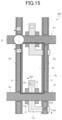
- FIG. 15 is a plan view schematically illustrating yet another liquid crystal display device 400 according to an embodiment of the present invention and illustrates a region corresponding to one pixel of the liquid crystal display device 400 .
- FIG. 16 is a cross-sectional view schematically illustrating the liquid crystal display device 400 and illustrates a cross section along the line 16 A- 16 A′ in FIG. 15 .
- FIG. 17 is a cross-sectional view schematically illustrating the liquid crystal display device 400 and illustrates a cross section along the line 17 A- 17 A′ in FIG. 15 .
- FIG. 1 is a plan view schematically illustrating the liquid crystal display device 100 and illustrates a region corresponding to one pixel in the liquid crystal display device 100 .
- FIG. 2 and FIG. 3 are cross-sectional views schematically illustrating the liquid crystal display device 100 and illustrate cross sections along the lines 2 A- 2 A′ and 3 A- 3 A′ in FIG. 1 , respectively.
- the liquid crystal display device 100 includes an active matrix substrate 1 , a counter substrate 2 facing the active matrix substrate 1 , and a liquid crystal layer 3 provided between the active matrix substrate 1 and the counter substrate 2 .
- the liquid crystal display device 100 includes a plurality of pixels. The plurality of pixels are arranged in a matrix shape including a plurality of rows and a plurality of columns.
- the liquid crystal display device 100 is typically further provided with a backlight (illumination device) disposed on a back face side (opposite to a viewer) of the active matrix substrate 1 .
- the active matrix substrate 1 includes a first substrate 10 and an oxide semiconductor thin film transistor (TFT) 11 supported by the first substrate 10 and disposed in each pixel. Further, the active matrix substrate 1 includes a plurality of gate wiring lines GL extending in a row direction and a plurality of source wiring lines SL extending in a column direction.
- TFT oxide semiconductor thin film transistor
- the first substrate 10 is transparent and has insulating properties.
- the first substrate 10 is, for example, a glass substrate or a plastic substrate.
- the oxide semiconductor TFT 11 includes an oxide semiconductor layer 11 o , a gate insulating layer GI provided on the oxide semiconductor layer 11 o , a gate electrode 11 g facing the oxide semiconductor layer 11 o with the gate insulating layer GI interposed therebetween, and a source electrode 11 s electrically connected to the oxide semiconductor layer 11 o.
- the oxide semiconductor layer 11 o includes a channel region 11 oc , and a source region 11 os and a drain region 11 od that are positioned respectively on both sides of the channel region 11 oc .
- the channel region 11 oc overlaps the gate electrode 11 g.
- a light blocking layer 12 is provided below the channel region 11 oc .
- the light blocking layer 12 overlaps at least the channel region 11 oc when viewed from the normal direction of the display surface.
- the light blocking layer 12 is formed of, for example, a metal material.
- a lower insulating layer 13 is provided covering the light blocking layer 12 .
- the oxide semiconductor layer 11 o is provided on the lower insulating layer 13 .
- a silicon oxide (SiO 2 ) layer or a silicon nitride (SiNx) layer can be used, for example.
- the lower insulating layer 13 may have a layered structure. For example, a silicon nitride layer may be included as a lower layer and a silicon oxide layer may be included as an upper layer.
- oxidation defects occurring in the channel region 11 oc of the oxide semiconductor layer 11 o can be reduced by the oxide film, and thus lowering of the resistance of the channel region can be suppressed.
- the source electrode 11 s is provided on the lower insulating layer 13 .
- the source electrode 11 s is electrically connected to the source region 11 os of the oxide semiconductor layer 11 o .
- a portion of a lower face of the source region 11 os and an upper face of the source electrode 11 s come into contact with each other, thereby electrically connecting the source region 11 os and the source electrode 11 s.
- the insulating layer illustrated as a specific example of the lower insulating layer 13 can be used.
- an oxide layer such as a silicon oxide layer is used as the gate insulating layer GI (or, the bottom layer of the gate insulating layer GI in a case where the gate insulating layer GI has a layered structure)
- oxidation defects produced in the channel region 11 oc can be reduced by the oxide film.
- the plurality of gate wiring lines GL are formed of the same conductive film (gate metal film) as the gate electrode 11 g .
- the gate electrode 11 g is integrally formed with any one of the plurality of gate wiring lines GL, and a portion of each gate wiring line GL overlapping the oxide semiconductor layer 11 o functions as the gate electrode 11 g.
- the plurality of source wiring lines SL are positioned closer to the first substrate 10 than the plurality of gate wiring lines GL. Specifically, the plurality of source wiring lines SL are provided on the lower insulating layer 13 . More specifically, the plurality of source wiring lines SL are provided between the lower insulating layer 13 and the gate insulating layer GI. In the illustrated example, the source electrode 11 s is integrally formed with any one of the plurality of source wiring lines SL, and a portion of each source wiring line SL overlapping (coming into contact with) the oxide semiconductor layer 11 o functions as the source electrode 11 s.
- the interlayer insulating layer 14 is provided covering the plurality of gate wiring lines GL and the oxide semiconductor TFT 11 .
- the interlayer insulating layer 14 is, for example, an organic insulating layer, but may also be an inorganic insulating layer.
- a photosensitive resin material is used, for example.
- a pixel electrode 15 is provided on the interlayer insulating layer 14 .
- the pixel electrode 15 is formed of a transparent conductive material (indium tin oxide (ITO), for example).
- ITO indium tin oxide
- the pixel electrode 15 is electrically connected to the drain region 11 od of the oxide semiconductor layer 11 o .
- the pixel electrode 15 is in contact with the drain region 11 od in a contact hole CH formed in the gate insulating layer GI and the interlayer insulating layer 14 . That is, the pixel electrode 15 is directly connected to the drain region 11 od without a drain electrode formed of a metal material interposed therebetween. Slits and openings may be formed in the pixel electrode 15 in accordance with the display mode used.
- a first alignment film 16 is provided on an outermost surface of the active matrix substrate 1 and comes into contact with the liquid crystal layer 3 .
- a horizontal alignment film or a vertical alignment film is used in accordance with the display mode.
- the counter substrate 2 includes a second substrate 20 and a plurality of columnar spacers 21 provided on the second substrate 20 .
- the counter substrate 2 typically further includes a color filter and a black matrix.
- the second substrate 20 is transparent and has insulating properties.
- the second substrate 20 is, for example, a glass substrate or a plastic substrate.
- the plurality of columnar spacers 21 define the thickness (cell gap) of the liquid crystal layer 3 .
- the plurality of columnar spacers 21 are typically formed of a photosensitive resin material and may be referred to as “photo spacers”.
- a second alignment film 26 is provided on an outermost surface of the counter substrate 2 and comes into contact with the liquid crystal layer 3 .
- a horizontal alignment film or a vertical alignment film is used in accordance with the display mode.
- one of the active matrix substrate 1 and the counter substrate 2 further includes a common electrode to which a common voltage is applied.
- a common electrode is provided to the counter substrate 2
- a common electrode is provided to the active matrix substrate 1 .
- the liquid crystal display device 100 includes a pair of polarizers that face each other with at least the liquid crystal layer 3 interposed therebetween.
- one of the pair of polarizers is disposed on the back face side of the active matrix substrate 1 , and the other is disposed on a front face side of the counter substrate 2 .
- each of the plurality of columnar spacers 21 is disposed in a region (hereinafter referred to as an “intersecting region”) where any one of the plurality of gate wiring lines GL and any one of the plurality of source wiring lines SL intersect. Note that the columnar spacers 21 need not be disposed in all of the plurality of intersecting regions.
- the arrangement density of each columnar spacer 21 is set as appropriate according to specifications and applications of the liquid crystal display device 100 .
- a front face of the active matrix substrate 1 on the liquid crystal layer 3 side includes a plurality of first ridges P 1 overlapping the plurality of gate wiring lines GL when viewed from the normal direction of the display surface, and a plurality of second ridges P 2 overlapping the plurality of source wiring lines SL when viewed from the normal direction of the display surface.
- the first ridge P 1 is a portion raised above the other portions (portions other than the first ridge P 1 and the second ridge P 2 ) due to the thickness of the gate wiring line GL.
- the gate wiring line GL is positioned on the upper layer side of the source wiring line SL, and thus the shape of the gate wiring line GL is readily reflected in the front face of the active matrix substrate 1 on the liquid crystal layer 3 side.
- the active matrix substrate 1 includes a plurality of base conductive layers 17 provided below the interlayer insulating layer 14 .
- the plurality of base conductive layers 17 overlap the plurality of second ridges P 2 when viewed from the normal direction of the display surface.
- the second ridge P 2 is a portion raised above the other portions (portions other than the first ridge P 1 and the second ridge P 2 ) due to the thickness of the base conductive layer 17 .
- the plurality of base conductive layers 17 are formed of the same conductive film (that is, a gate metal film) as the plurality of gate wiring lines GL. Accordingly, the thickness of the base conductive layer 17 and the thickness of the gate wiring line GL are substantially the same. The thicknesses of the base conductive layer 17 and the gate wiring line GL are, for example, greater than or equal to 100 nm and less than or equal to 500 nm. Further, the plurality of base conductive layers 17 are not electrically connected to the plurality of gate wiring lines GL, and are electrically floating.
- FIG. 4 is a plan view schematically illustrating the liquid crystal display device 900 and illustrates a region corresponding to one pixel in the liquid crystal display device 900 .
- FIG. 5 is a cross-sectional view schematically illustrating the liquid crystal display device 900 and illustrates a cross section along the line 5 A- 5 A′ in FIG. 4 .
- the active matrix substrate 1 of the liquid crystal display device 900 of the comparative example has a lower source structure. That is, the source wiring line SL is positioned closer to the first substrate 10 than the gate wiring line GL. In other words, the gate wiring line GL is positioned on the upper layer side of the source wiring line SL. Therefore, the front face of the active matrix substrate 1 on the liquid crystal layer 3 side includes the plurality of first ridges P 1 raised due to the thickness of the plurality of gate wiring lines GL. Needless to say, the plurality of first ridges P 1 overlap the plurality of gate wiring lines GL when viewed from the normal direction of the display surface.
- the base conductive layer 17 is not provided below the interlayer insulating layer 14 . Therefore, the front face of the active matrix substrate 1 of the liquid crystal display device 900 on the liquid crystal layer 3 side does not include the second ridges P 2 (raised portions due to the thickness of the base conductive layer 17 ).
- each of the plurality of columnar spacers 21 is disposed in the intersecting region (the region where the gate wiring line GL and the source wiring line SL intersect).
- the position of the columnar spacer 21 may be offset due to externally applied stress. Due to such a positional offset, when the columnar spacer 21 deviates from the intersecting region, that is, when the columnar spacer 21 falls to a position offset from the first ridge P 1 , there is a risk that scratches caused by the columnar spacer 21 may occur in the alignment film 16 in a region that contributes to the display. Scratches are visible as brush-like marks at the time of black display.
- the front face of the active matrix substrate 1 on the liquid crystal layer 3 side includes, in addition to the plurality of first ridges P 1 , the plurality of second ridges P 2 overlapping the plurality of source wiring lines SL when viewed from the normal direction of the display surface.
- a cross-sectional shape of the columnar spacer 21 (the shape in a cross section parallel to the first substrate 10 ) may be any of various shapes, such as a perfect circle, a square, or the like.
- a height h 2 (refer to FIG. 3 ) of each of the plurality of second ridges P 2 is preferably greater than or equal to a height h 1 (refer to FIG. 3 ) of each of the plurality of first ridges P 1 .
- the height h 1 of the first ridge P 1 and the height h 2 of the second ridge P 2 are each a distance from a planar face (here, a front face of the first substrate 10 ) serving as a reference to a peak face of the first ridge P 1 or the second ridge P 2 .
- the height h 2 of each of the plurality of second ridges P 2 is preferably greater than the height h 1 of each of the plurality of first ridges P 1 , and more preferably greater than or equal to 20 nm.
- forming the plurality of base conductive layers 17 of the same conductive film as the plurality of gate wiring lines GL creates the advantage that it is not necessary to add a step of forming the base conductive layer 17 when manufacturing the liquid crystal display device 100 .
- each of the base conductive layers 17 may be electrically connected to any one of the plurality of gate wiring lines GL.
- the plurality of base conductive layers 17 are preferably not electrically connected to the plurality of gate wiring lines GL.
- a width w 2 (refer to FIG. 2 ) of each of the plurality of base conductive layers 17 is preferably less than or equal to a width w 1 (refer to FIG. 2 ) of each of the plurality of source wiring lines SL.
- the width w 2 of the base conductive layer 17 is greater than the width w 1 of the source wiring line SL, the aperture ratio may decrease.
- the width w 2 of the base conductive layer 17 is too small, the second ridge P 2 may not be appropriately formed with a sufficient width.
- the width w 2 of the base conductive layer 17 is preferably smaller than the width w 1 of the source wiring line SL by an amount greater than or equal to 0 ⁇ m and less than or equal to 1 ⁇ m.
- FIG. 10 is a plan view schematically illustrating the liquid crystal display device 200 and illustrates a region corresponding to one pixel in the liquid crystal display device 200 .
- FIG. 11 is a cross-sectional view schematically illustrating the liquid crystal display device 200 and illustrates a cross section along the line 11 A- 11 A′ in FIG. 10 .
- the following description will focus on differences between the liquid crystal display device 200 and the liquid crystal display device 100 of the first embodiment.
- the liquid crystal display device 200 of the present embodiment differs from the liquid crystal display device 100 of the first embodiment in that a plurality of base conductive layers 17 ′ are formed of a conductive film different from that of the plurality of gate wiring lines GL. Further, in the illustrated example, a thickness t 2 of the base conductive layer 17 ′ is greater than a thickness t 1 of the gate wiring line GL, and the height h 2 of the second ridge P 2 is greater than the height h 1 of the first ridge P 1 .
- the thickness t 2 of the base conductive layer 17 ′ can be set independently of (that is, different from) the thickness t 1 of the gate wiring line GL. Accordingly, it is easier to control the height h 2 of the second ridge P 2 . Therefore, it is easier to realize a configuration in which the height h 2 of the second ridge P 2 is greater than the height h 1 of the first ridge P 1 . With the height h 2 of the second ridge P 2 greater than the height h 1 of the first ridge P 1 , it is possible prevent a positional offset of the columnar spacer 21 .
- the height h 2 of the second ridge P 2 can be made greater than the height h 1 of the first ridge P 1 by making the thickness t 2 of the base conductive layer 17 ′ greater than the thickness t 1 of the gate wiring line GL. From the perspective of more reliably achieving a configuration in which the height h 2 of the second ridge P 2 is greater than the height h 1 of the first ridge P 1 , the thickness t 2 of the base conductive layer 17 ′ is preferably made greater than the thickness t 1 of the gate wiring line GL by 50 nm or more.
- the conductive material that forms the base conductive layer 17 ′ is not particularly limited, and various metal materials can be used.
- FIG. 12 is a plan view schematically illustrating the liquid crystal display device 300 and illustrates a region corresponding to one pixel in the liquid crystal display device 300 .
- FIG. 13 and FIG. 14 are cross-sectional views schematically illustrating the liquid crystal display device 300 and illustrate cross sections along the lines 13 A- 13 A′ and 14 A- 14 A′ in FIG. 12 , respectively.
- the following description will focus on differences between the liquid crystal display device 300 and the liquid crystal display device 100 of the first embodiment.
- the active matrix substrate 1 of the liquid crystal display device 300 in the present embodiment is different from those of the liquid crystal display devices 100 , 200 of the first and second embodiments, and does not include the base conductive layer 17 , 17 ′. Further, the active matrix substrate 1 of the liquid crystal display device 300 includes a plurality of transparent insulating layers 18 provided above the interlayer insulating layer 14 . The plurality of transparent insulating layers 18 overlap the plurality of second ridges P 2 when viewed from the normal direction of the display surface. Each second ridge P 2 is raised above the other portions (portions other than the first ridge P 1 and the second ridge P 2 ) due to the thickness of the transparent insulating layer 18 . In the example illustrated, the transparent insulating layer 18 is not formed in the intersecting region (the region where any one of the plurality of gate wiring lines GL and any one of the plurality of source wiring lines SL intersect).
- the second ridge P 2 is formed by the transparent insulating layer 18 provided above the interlayer insulating layer 14 , and thus the aperture ratio does not decrease even when a width w 3 of the transparent insulating layer 18 is greater than the width w 1 of the source wiring line SL. Further, even when the transparent insulating layer 18 overlaps the source wiring line SL, the parasitic capacitance of the source wiring line SL is not increased, and thus load of the source wiring line SL does not increase. Furthermore, the thickness t 3 of the transparent insulating layer 18 can be set independently of the thickness t 1 of the gate wiring line GL, making it easier to control the height h 2 of the second ridge P 2 .
- the height h 2 of the second ridge P 2 is greater than the height h 1 of the first ridge P 1 .
- the height h 2 of the second ridge P 2 can be made greater than the height h 1 of the first ridge P 1 by making the thickness t 3 of the transparent insulating layer 18 greater than the thickness t 1 of the gate wiring line GL.
- the transparent insulating layer 18 when the transparent insulating layer 18 is formed in the intersecting region, a height of the front face of the active matrix substrate 1 on the liquid crystal layer 3 side may be highest in the intersecting region. Therefore, the transparent insulating layer 18 is preferably not formed in the intersecting region.
- a photosensitive resin material can be used, for example.
- the width w 3 of the transparent insulating layer 18 is not particularly limited, but when the width w 3 of the transparent insulating layer 18 is too small, there is a risk that the second ridge P 2 cannot be suitably formed with sufficient width, and thus the width w 3 [ ⁇ m] of the transparent insulating layer 18 preferably satisfies the relationship w 3 ⁇ w 1 ⁇ 1 with the width w 1 [ ⁇ m] of the source wiring line SL.
- the transparent insulating layer 18 may be provided below the interlayer insulating layer 14 , and more specifically, between the gate insulating layer GI and the interlayer insulating layer 14 .
- a configuration in which the transparent insulating layer 18 is provided above the interlayer insulating layer 14 makes it easier to control the height h 2 of the second ridge P 2 .
- FIG. 15 is a plan view schematically illustrating the liquid crystal display device 400 and illustrates a region corresponding to one pixel in the liquid crystal display device 400 .
- FIG. 16 and FIG. 17 are cross-sectional views schematically illustrating the liquid crystal display device 400 and illustrate cross sections along the lines 16 A- 16 A′ and 17 A- 17 A′ in FIG. 15 , respectively.
- the following description will focus on differences between the liquid crystal display device 400 and the liquid crystal display device 100 of the first embodiment.
- the plurality of source wiring lines SL are provided on the lower insulating layer 13 .
- the plurality of source wiring lines SL are provided below the lower insulating layer 13 .
- the plurality of source wiring lines SL are covered by the lower insulating layer 13 .
- the light blocking layer 12 is formed of the same conductive film as the plurality of source wiring lines SL.
- the oxide semiconductor layer 11 o is provided on the lower insulating layer 13 .
- the source region 11 os and the source electrode 11 s of the oxide semiconductor layer 11 o are connected in a contact hole CHs formed in the lower insulating layer 13 .
- the manufacturing process can be simplified compared to a configuration in which the source wiring line SL and the light blocking layer 12 are formed in different layers (that is, formed of different conductive films), as in the liquid crystal display device 100 of the first embodiment.
- the source wiring line SL and the light blocking layer 12 are formed of the same conductive film, in order to make the source wiring line SL and the light blocking layer 12 not electrically connected to each other (not conductive), spacing between the source wiring line SL and the light blocking layer 12 needs to be greater than or equal to a predetermined size. Therefore, in a high definition liquid crystal display device, it can be said that it is preferable to adopt a configuration in which the source wiring line SL and the light blocking layer 12 are formed in different layers as in the first embodiment.
- the base conductive layer 17 ′ formed of a conductive film different from that of the gate wiring line GL may be provided, similar to the liquid crystal display device 200 of the second embodiment.
- the transparent insulating layer 18 may be provided in place of the base conductive layer 17 , as in the liquid crystal display device 300 of the third embodiment.
- the occurrence of scratches in the alignment film 16 caused by the columnar spacer 21 can be prevented.
- the configuration for forming the second ridge P 2 is not limited to a configuration in which the base conductive layer 17 , 17 ′ such as illustrated are provided, or a configuration in which the transparent insulating layer 18 is provided.
- a finishing treatment may be performed.
- the film thickness of portions other than the second ridge P 2 may be reduced to a target film thickness by, for example, forming the interlayer insulating layer 14 thicker than the target film thickness in advance and then etching with the portion corresponding to the second ridge P 2 covered by a mask.
- the oxide semiconductor contained in the oxide semiconductor layer 11 o may be an amorphous oxide semiconductor or may be a crystalline oxide semiconductor including a crystalline portion.
- Examples of the crystalline oxide semiconductor include a polycrystalline oxide semiconductor, a microcrystalline oxide semiconductor, or a crystalline oxide semiconductor having a c-axis oriented substantially perpendicular to the layer surface.
- the oxide semiconductor layer 11 o may have a layered structure of two or more layers.
- the oxide semiconductor layer 11 o may include an amorphous oxide semiconductor layer and a crystalline oxide semiconductor layer.
- the oxide semiconductor layer 11 o may include a plurality of crystalline oxide semiconductor layers having different crystal structures.
- the oxide semiconductor layer 11 o may include a plurality of amorphous oxide semiconductor layers.
- an energy gap of the oxide semiconductor included in the lower layer is preferably greater than an energy gap of the oxide semiconductor included in the upper layer.
- the energy gap of the oxide semiconductor in the upper layer may be greater than the energy gap of the oxide semiconductor in the lower layer.
- JP 2014-007399 A Materials, structures, and film formation methods of an amorphous oxide semiconductor and the above-described crystalline oxide semiconductors, a configuration of an oxide semiconductor layer including a layered structure, and the like are described in, for example, JP 2014-007399 A. The entire contents of the disclosure of JP 2014-007399 A are incorporated herein as reference.
- the oxide semiconductor layer 11 o may include, for example, at least one metal element selected from In, Ga, and Zn.
- the oxide semiconductor layer 11 o includes, for example, an In—Ga—Zn—O based semiconductor (for example, an indium gallium zinc oxide).
- the In—Ga—Zn—O based semiconductor is a ternary oxide of In (indium), Ga (gallium), and Zn (zinc), and a ratio (composition ratio) of In, Ga, and Zn is not particularly limited.
- Such an oxide semiconductor layer 11 o can be formed of an oxide semiconductor film including an In—Ga—Zn—O based semiconductor.
- the In—Ga—Zn—O based semiconductor may be an amorphous semiconductor or may be a crystalline semiconductor.
- a crystalline In—Ga—Zn—O based semiconductor in which a c-axis is oriented substantially perpendicular to a layer surface is preferable as the crystalline In—Ga—Zn—O based semiconductor.
- JP 2014-007399 A, JP 2012-134475 A, and JP 2014-209727 A as described above.
- the entire contents of the disclosure of JP 2012-134475 A and JP 2014-209727 A are incorporated herein as reference.
- a TFT including an In—Ga—Zn—O based semiconductor layer has high mobility (more than 20 times as compared to an a-Si TFT) and a low leakage current (less than 1/100th as compared to the a-Si TFT), and thus such a TFT can be used suitably as a driving TFT (for example, a TFT present in a drive circuit provided in a periphery of a display region including a plurality of pixels, and on the same substrate as the display region) and a pixel TFT (TFT provided in a pixel).
- a driving TFT for example, a TFT present in a drive circuit provided in a periphery of a display region including a plurality of pixels, and on the same substrate as the display region
- TFT provided in a pixel
- the oxide semiconductor layer 11 o may include another oxide semiconductor.
- the oxide semiconductor layer 11 o may include an In—Sn—Zn—O based semiconductor (for example, In 2 O 3 —SnO 2 —ZnO; InSnZnO).
- the In—Sn—Zn—O based semiconductor is a ternary oxide of In (indium), Sn (tin), and Zn (zinc).
- the oxide semiconductor layer 11 o may include an In—Al—Zn—O based semiconductor, an In—Al—Sn—Zn—O based semiconductor, a Zn—O based semiconductor, an In—Zn—O based semiconductor, a Zn—Ti—O based semiconductor, a Cd—Ge—O based semiconductor, a Cd—Pb—O based semiconductor, CdO (cadmium oxide), a Mg—Zn—O based semiconductor, an In—Ga—Sn—O based semiconductor, an In—Ga—O based semiconductor, a Zr—In—Zn—O based semiconductor, a Hf—In—Zn—O based semiconductor, an Al—Ga—Zn—O based semiconductor, a Ga—Zn—O based semiconductor, an In—Ga—Zn—Sn—O based semiconductor, and the like.
Landscapes
- Physics & Mathematics (AREA)
- Nonlinear Science (AREA)
- Mathematical Physics (AREA)
- Chemical & Material Sciences (AREA)
- Crystallography & Structural Chemistry (AREA)
- General Physics & Mathematics (AREA)
- Optics & Photonics (AREA)
- Engineering & Computer Science (AREA)
- Microelectronics & Electronic Packaging (AREA)
- Spectroscopy & Molecular Physics (AREA)
- Liquid Crystal (AREA)
Abstract
Description
Claims (17)
Priority Applications (1)
| Application Number | Priority Date | Filing Date | Title |
|---|---|---|---|
| US16/935,239 US11226529B2 (en) | 2019-07-26 | 2020-07-22 | Liquid crystal display device |
Applications Claiming Priority (2)
| Application Number | Priority Date | Filing Date | Title |
|---|---|---|---|
| US201962878772P | 2019-07-26 | 2019-07-26 | |
| US16/935,239 US11226529B2 (en) | 2019-07-26 | 2020-07-22 | Liquid crystal display device |
Publications (2)
| Publication Number | Publication Date |
|---|---|
| US20210026211A1 US20210026211A1 (en) | 2021-01-28 |
| US11226529B2 true US11226529B2 (en) | 2022-01-18 |
Family
ID=74190749
Family Applications (1)
| Application Number | Title | Priority Date | Filing Date |
|---|---|---|---|
| US16/935,239 Active US11226529B2 (en) | 2019-07-26 | 2020-07-22 | Liquid crystal display device |
Country Status (2)
| Country | Link |
|---|---|
| US (1) | US11226529B2 (en) |
| CN (1) | CN112305819B (en) |
Families Citing this family (4)
| Publication number | Priority date | Publication date | Assignee | Title |
|---|---|---|---|---|
| CN212846287U (en) | 2020-09-11 | 2021-03-30 | 北京京东方显示技术有限公司 | Display panel and display device |
| JP2022178523A (en) * | 2021-05-20 | 2022-12-02 | シャープディスプレイテクノロジー株式会社 | Active matrix substrate and liquid crystal display device |
| CN114296282A (en) * | 2022-01-06 | 2022-04-08 | 昆山龙腾光电股份有限公司 | Array substrate, manufacturing method and display panel |
| JP2024162199A (en) * | 2023-05-09 | 2024-11-21 | シャープディスプレイテクノロジー株式会社 | Liquid crystal display panel, display device, and active matrix substrate manufacturing method |
Citations (8)
| Publication number | Priority date | Publication date | Assignee | Title |
|---|---|---|---|---|
| US20100201933A1 (en) * | 2009-02-09 | 2010-08-12 | Hitachi Displays, Ltd. | Liquid crystal display device |
| US20120138922A1 (en) | 2010-12-03 | 2012-06-07 | Semiconductor Energy Laboratory Co., Ltd. | Oxide semiconductor film and semiconductor device |
| US20130320334A1 (en) | 2012-05-31 | 2013-12-05 | Semiconductor Energy Laboratory Co., Ltd. | Semiconductor device |
| US20140286076A1 (en) | 2013-03-25 | 2014-09-25 | Semiconductor Energy Laboratory Co., Ltd. | Semiconductor device |
| JP2015109315A (en) | 2013-12-03 | 2015-06-11 | 出光興産株式会社 | THIN FILM TRANSISTOR, MANUFACTURING METHOD THEREOF, OXIDE SEMICONDUCTOR LAYER, DISPLAY DEVICE AND SEMICONDUCTOR DEVICE |
| WO2015186619A1 (en) | 2014-06-06 | 2015-12-10 | シャープ株式会社 | Semiconductor device, display device and method for manufacturing semiconductor device |
| US20170285393A1 (en) * | 2016-04-04 | 2017-10-05 | Samsung Display Co., Ltd. | Display device |
| US20190196257A1 (en) * | 2016-05-04 | 2019-06-27 | Samsung Display Co., Ltd. | Display device having a non-rectilinear display area |
Family Cites Families (2)
| Publication number | Priority date | Publication date | Assignee | Title |
|---|---|---|---|---|
| WO2012147722A1 (en) * | 2011-04-26 | 2012-11-01 | シャープ株式会社 | Liquid crystal display device |
| CN107636841B (en) * | 2015-06-05 | 2020-10-09 | 夏普株式会社 | Active matrix substrate, manufacturing method thereof, and display device using active matrix substrate |
-
2020
- 2020-07-22 US US16/935,239 patent/US11226529B2/en active Active
- 2020-07-22 CN CN202010712534.2A patent/CN112305819B/en active Active
Patent Citations (12)
| Publication number | Priority date | Publication date | Assignee | Title |
|---|---|---|---|---|
| US20100201933A1 (en) * | 2009-02-09 | 2010-08-12 | Hitachi Displays, Ltd. | Liquid crystal display device |
| US20120138922A1 (en) | 2010-12-03 | 2012-06-07 | Semiconductor Energy Laboratory Co., Ltd. | Oxide semiconductor film and semiconductor device |
| JP2012134475A (en) | 2010-12-03 | 2012-07-12 | Semiconductor Energy Lab Co Ltd | Oxide semiconductor film and semiconductor device |
| US20130320334A1 (en) | 2012-05-31 | 2013-12-05 | Semiconductor Energy Laboratory Co., Ltd. | Semiconductor device |
| JP2014007399A (en) | 2012-05-31 | 2014-01-16 | Semiconductor Energy Lab Co Ltd | Semiconductor device |
| US20140286076A1 (en) | 2013-03-25 | 2014-09-25 | Semiconductor Energy Laboratory Co., Ltd. | Semiconductor device |
| JP2014209727A (en) | 2013-03-25 | 2014-11-06 | 株式会社半導体エネルギー研究所 | Semiconductor device |
| JP2015109315A (en) | 2013-12-03 | 2015-06-11 | 出光興産株式会社 | THIN FILM TRANSISTOR, MANUFACTURING METHOD THEREOF, OXIDE SEMICONDUCTOR LAYER, DISPLAY DEVICE AND SEMICONDUCTOR DEVICE |
| WO2015186619A1 (en) | 2014-06-06 | 2015-12-10 | シャープ株式会社 | Semiconductor device, display device and method for manufacturing semiconductor device |
| US20170090229A1 (en) | 2014-06-06 | 2017-03-30 | Sharp Kabushiki Kaisha | Semiconductor device, display device and method for manufacturing semiconductor device |
| US20170285393A1 (en) * | 2016-04-04 | 2017-10-05 | Samsung Display Co., Ltd. | Display device |
| US20190196257A1 (en) * | 2016-05-04 | 2019-06-27 | Samsung Display Co., Ltd. | Display device having a non-rectilinear display area |
Also Published As
| Publication number | Publication date |
|---|---|
| US20210026211A1 (en) | 2021-01-28 |
| CN112305819A (en) | 2021-02-02 |
| CN112305819B (en) | 2024-04-02 |
Similar Documents
| Publication | Publication Date | Title |
|---|---|---|
| US11226529B2 (en) | Liquid crystal display device | |
| US8071985B2 (en) | Display device and method of manufacturing the same | |
| US10978529B2 (en) | Active matrix substrate and method for manufacturing the same | |
| CN103946741B (en) | The manufacture method of active-matrix substrate, liquid crystal indicator and active-matrix substrate | |
| KR102182482B1 (en) | OXIDE SEMlCONDUCTOR THIN FILM TRANSISTOR AND ARRAY SUBSTRATE FOR DISPLAY DEVICE HAVING THE SAME | |
| US8310613B2 (en) | Active matrix substrate and liquid crystal device | |
| US11079644B2 (en) | Liquid crystal display device and manufacturing method of the same | |
| US9570469B2 (en) | Active-matrix substrate and liquid-crystal display device | |
| US12313948B2 (en) | Active matrix substrate and liquid crystal display device | |
| US8665413B2 (en) | Thin film transistor array panel, liquid crystal display, and manufacturing method thereof | |
| US20200124891A1 (en) | Active matrix substrate, liquid crystal display panel, and method for manufacturing liquid crystal display panel | |
| US10698283B2 (en) | Liquid crystal display device | |
| US7777230B2 (en) | Display device | |
| US10976626B2 (en) | Display device | |
| JP4703258B2 (en) | Thin film transistor substrate and liquid crystal display panel | |
| TWI451177B (en) | Active device, pixel structure, driving circuit and display panel | |
| CN117690930A (en) | Active matrix substrate and liquid crystal display device | |
| US9726953B2 (en) | Active matrix substrate and liquid-crystal display device | |
| US20200004073A1 (en) | Liquid crystal display device | |
| US20190179181A1 (en) | Liquid crystal display device | |
| US20250287693A1 (en) | Active matrix substrate, display device and method for manufacturing active matrix substrate | |
| US12117706B2 (en) | Active matrix substrate and liquid crystal display device | |
| US20250294881A1 (en) | Active matrix substrate and liquid crystal display device | |
| US20240337885A1 (en) | Active matrix substrate and liquid crystal display device | |
| JPWO2018181142A1 (en) | Active matrix substrate, liquid crystal display |
Legal Events
| Date | Code | Title | Description |
|---|---|---|---|
| AS | Assignment |
Owner name: SHARP KABUSHIKI KAISHA, JAPAN Free format text: ASSIGNMENT OF ASSIGNORS INTEREST;ASSIGNORS:YOSHIDA, KEISUKE;TANAKA, KOHHEI;REEL/FRAME:053274/0460 Effective date: 20190723 |
|
| FEPP | Fee payment procedure |
Free format text: ENTITY STATUS SET TO UNDISCOUNTED (ORIGINAL EVENT CODE: BIG.); ENTITY STATUS OF PATENT OWNER: LARGE ENTITY |
|
| STPP | Information on status: patent application and granting procedure in general |
Free format text: DOCKETED NEW CASE - READY FOR EXAMINATION |
|
| STPP | Information on status: patent application and granting procedure in general |
Free format text: NON FINAL ACTION MAILED |
|
| STPP | Information on status: patent application and granting procedure in general |
Free format text: RESPONSE TO NON-FINAL OFFICE ACTION ENTERED AND FORWARDED TO EXAMINER |
|
| STPP | Information on status: patent application and granting procedure in general |
Free format text: NOTICE OF ALLOWANCE MAILED -- APPLICATION RECEIVED IN OFFICE OF PUBLICATIONS |
|
| STPP | Information on status: patent application and granting procedure in general |
Free format text: PUBLICATIONS -- ISSUE FEE PAYMENT VERIFIED |
|
| STCF | Information on status: patent grant |
Free format text: PATENTED CASE |
|
| MAFP | Maintenance fee payment |
Free format text: PAYMENT OF MAINTENANCE FEE, 4TH YEAR, LARGE ENTITY (ORIGINAL EVENT CODE: M1551); ENTITY STATUS OF PATENT OWNER: LARGE ENTITY Year of fee payment: 4 |