CROSS-REFERENCE TO RELATED APPLICATIONS
The present disclosure is a continuation of co-pending U.S. patent application Ser. No. 16/546,084, filed on Aug. 20, 2019, which is incorporated herein by reference in its entirety.
TECHNICAL FIELD
Embodiments presented in this disclosure generally relate to fabricating features in optoelectronic devices. More specifically, embodiments disclosed herein provide for the production of waveguide and mirrors in the light path of the waveguides to redirect the light path.
BACKGROUND
Waveguides are optical components that confine and direct the path that light travels within the medium of an optical device. The optical waveguides define areas of increased refractive index relative to the optical medium (e.g., SiO2) to direct the light along a desired trajectory. Due to the refractive index difference of the waveguides relative to bulk material of the optical device, waveguides can define curved paths that gradually shift the light from one straight path to another.
BRIEF DESCRIPTION OF THE DRAWINGS
So that the manner in which the above-recited features of the present disclosure can be understood in detail, a more particular description of the disclosure, briefly summarized above, may be had by reference to embodiments, some of which are illustrated in the appended drawings. It is to be noted, however, that the appended drawings illustrate typical embodiments and are therefore not to be considered limiting; other equally effective embodiments are contemplated.
FIG. 1 illustrates a cutaway view of a periscope assembly, according to embodiments of the present disclosure.
FIG. 2 illustrates a cutaway view of a two-piece periscope assembly, according to embodiments of the present disclosure.
FIG. 3 illustrates a series of mirrors of different layouts, according to embodiments of the present disclosure.
FIGS. 4A-4C illustrate several alignments of two mirrors and three associated waveguides. According to embodiments of the present disclosure.
FIG. 5 illustrates a reordered waveguide layout, according to embodiments of the present disclosure.
FIG. 6 illustrates a mirror arrangement, according to embodiments of the present disclosure.
FIG. 7 illustrates a mirror arrangement, according to embodiments of the present disclosure.
FIG. 8 illustrates a mirror arrangement, according to embodiments of the present disclosure.
FIG. 9 illustrates a mirror arrangement, according to embodiments of the present disclosure.
FIG. 10 illustrates a mirror arrangement, according to embodiments of the present disclosure.
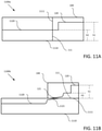
FIGS. 11A and 11B illustrate coupling arrangements for a periscope assembly and another optical element, according to embodiments of the present disclosure.
FIG. 12 is a flowchart of a method to deploy a periscope optical assembly.
To facilitate understanding, identical reference numerals have been used, where possible, to designate identical elements that are common to the figures. It is contemplated that elements disclosed in one embodiment may be beneficially used in other embodiments without specific recitation.
DESCRIPTION OF EXAMPLE EMBODIMENTS
Overview
One embodiment presented in this disclosure describes an interposer, comprising: a bulk material having a first side and a second side opposite to the first side; a first optic defined in the bulk material at a first height in the bulk material along an axis extending between the first second sides; a second optic defined in the bulk material at a second height in the bulk material, different than the first height, along the axis; a first waveguide defined in the bulk material, extending from the first side to the first optic; a second waveguide defined in the bulk material, extending from the second optic to the second side; and a third waveguide defined in the bulk material, extending from the first optic to the second optic.
One embodiment presented in this disclosure describes a method, comprising: defining a first mirror in a bulk material at a first height; defining a second mirror in the bulk material at a second height, different than the first height; defining a first waveguide in the bulk material, optically connected to the first mirror and a first edge of the bulk material; defining a second waveguide in the bulk material, optically connected to the second mirror and a second edge of the bulk material, different than the first edge; and defining a third waveguide in the bulk material, optically connected to the first mirror and the second mirror to define a light path from the first edge to the second edge via the first waveguide, the first mirror, the third waveguide, the second mirror, and the second waveguide.
One embodiment presented in this disclosure describes a system, comprising: a first waveguide defined in a first plane of a bulk material; a second waveguide defined in a second plane of the bulk material, parallel to the first plane; a third waveguide defined in a third plane of the bulk material that intersects the first plane and the second plane; a first mirror defined at a first intersection of the first plane and the third plane and optically connected to the first waveguide and the third waveguide; and a second mirror defined at a second intersection of the third plane and the second plane and optically connected to the third waveguide and the second waveguide.
Example Embodiments
The present disclosure provides systems and methods for the creation and deployment of periscope interposers and other optical devices using mirrors defined in the light paths of waveguides to rapidly and compactly redirect the direction in which light travels in the optical device. By defining at least a pair of mirrors in the light path, via etching, lithography, metal plating, chemical deposition, precision molding, and/or laser patterning, the periscope assembly can receive optical signals on one plane and redirect those optical signals to another plane, including planes parallel to the original plane, over a shorter distance than if the waveguide were curved to direct the optical signals to a new plane. Additionally, by staggering several mirrors, the waveguides can receive optical signals in a first physical arrangement, and output optical signals in a different physical arrangement.
Although the present disclosure generally provides examples related to interposers including mirrors and waveguides as internally defined components, the creation and deployment of periscope optical components can include additional optical and electrical elements, such as, for example, optical gratings, phase shifters, optical filters, and the like.
FIG. 1 illustrates a cutaway view of a periscope assembly 100 (e.g., an interposer), according to embodiments of the present disclosure. In various embodiments, the periscope assembly 100 of FIG. 1 is constructed as one component made of an optical bulk material 110, such as, for example, SiO2, in which a first waveguide 120 a (generally, waveguide 120), second waveguide 120 b, third waveguide, first mirror 130 a (generally, mirror 130), and second mirror 130 b are defined. In other embodiments, the periscope assembly 100 of FIG. 1 represents a fully constructed multi-piece periscope assembly, such as is discussed in greater detail in regard to FIG. 2.
Although generally described in relation to mirrors 130, the examples provided herein may be understood to include several other optics, including, but not limited to: mirrors, lenses, optical gratings, filters, and combinations thereof. The optics may be defined by various processes in the bulk material 110 to have different effects on optical signals carried in the bulk material 110 based on the refractive index and the angle of the light passing from one region in the bulk material 110 to another. For example, a waveguide 120 may be defined to confine light to a predefined path in the bulk material 110, whereas a mirror 130 may redirect light received in one direction to a second direction. Other optics may have other effects on light carried in the bulk material 110, such as a lens focusing/converging or diffusing/diverging incoming light, an optical grating splitting and diffracting light into several beams, a filter removing/blocking/attenuating/polarizing certain wavelengths of light, etc.
As illustrated in FIG. 1, a first waveguide 120 a runs in parallel to a second waveguide 120 b, and a third waveguide 120 c is optically coupled to the first and second waveguide 120 a-b via a first mirror 130 a and a second mirror 130 b. The first mirror 130 a is defined to receive optical signals carried on the first waveguide 120 a and reflect those optical signals onto the third waveguide 120 c. The second mirror 130 b is defined to receive the optical signals carried on the third waveguide 120 c and reflect those optical signals onto the second waveguide 120 b. The mirrors 130 may have various sizes, shapes, configurations of reflective surface, and interfaces with the waveguides 120 (e.g., lenses, filters) in various embodiments.
FIG. 2 illustrates a cutaway view of a two-part periscope assembly 200, which, when assembled, may provide the periscope assembly 100 illustrated in FIG. 1. As illustrated in FIG. 2, a first component 210 a includes a first waveguide 120 a, a second waveguide 120 b, and a first mirror 130 a disposed between the first waveguide 120 a and the second waveguide 120 b that are defined in the bulk material 110 of the first component 210 a. A second component 210 b includes a third waveguide 120 c, a fourth waveguide 120 d, and a second mirror 130 b disposed between the third waveguide 120 c and the fourth waveguide 120 d that are defined in the bulk material 110 of the second component 210 b.
Various alignment features 220 a-d (generally, alignment feature 220), such as paired male and female interconnects, may be defined in and on the bulk materials 110 of the first and second components 210 a-b (generally, two components 210) to align the second waveguide 120 b and the third waveguide 120 c, so that when the two components 210 are joined together, the second and third waveguides 120 b-c define one continuous waveguide 120. In various embodiments, the two components 210 are joined together via an epoxy joint, solder, thermocompression, or a die level process to bond and secure the components together. In various embodiments, the alignment features 220 are designed to self-align relative to a paired alignment feature to align the waveguides 120 in the periscope. For example, the alignment features 220 may be formed as U-grooves, V-grooves, interlocking notches, trapezoidal features, etc.
In some embodiments, the waveguides 120 and mirrors 130 in FIGS. 1 and 2 may be defined within the bulk material 110 by a three-dimensional laser patterning process to affect the material matrix of the bulk material 110 and thereby the refractive index of the material to contain light on a defined pathway as a waveguide 120, or to reflect and sharply redirect the light onto a new pathway as a mirror 130. In some embodiments, the waveguides 120 and mirrors in FIGS. 1 and 2 are defined via a multilayered lithographic process, or with a combination of lithographic and laser patterning processes. For example, a fabricator may use laser patterning to define the paths of the waveguides 120, and a physical and/or chemical etching process to define the mirrors 130. Other techniques, such as grayscale lithography, can be used to pattern three-dimensionally sloped mirrors 130 and optics in the bulk material 110.
In some embodiments, the mirrors 130 are defined as three-dimensional reflective structures within the bulk material 110, while in other embodiments, the mirrors 130 are defined via a reflective surface treatment. For example, a laser can positively define the structure of a mirror 130 by imparting a region with a different refractive index from the bulk material 110 and the waveguides 120 to reflect optical signals applied thereto to a different waveguide 120. For example, a laser can alter the material matrix of a bulk material 110 such as SiO2 to impart a region with a different reflectivity to certain wavelengths of light. In another example, a lithographic etching process can negatively define the structure of a mirror 130 by removing bulk material 110, and a fabricator can polish or apply a reflective coating applied to a surface defined in the etched region to define the mirror 130. Additionally, although not illustrated, a fabricator may apply a surface treatment and/or a lens to the interfaces between two waveguides 120 to reduce back reflection and/or signal power loss when an optical signal transitions from one waveguide 120 to another. In additional embodiments, index matching epoxy or antireflective coatings can also be used to reduce back reflection.
FIG. 3 illustrates a series of mirrors 130 of different layouts, according to embodiments of the present disclosure. The first mirror 130 a includes a flat reflective surface 310, while the second mirror 130 b and third mirror 130 c include curved reflective surfaces 310. Each of the illustrated mirrors 130 may be understood to be a positively defined “prism” or a negatively defined “void”. When interpreted as a prism, a reflective surface 310 is defined on an “exterior” surface to reflect optical signals. When interpreted as a void, a series of walls define the void, and a reflective surface 310 is defined on one “interior” surface of a wall to reflect optical signals. Accordingly, the second mirror 130 b may be concave when defined by a prism structure and convex when defined by a void. Similarly, the third mirror 130 c may be convex when defined by a prism structures and concave when defined by a void. Although the present disclosure primarily illustrates the example mirrors 130 as including flat reflective surfaces 310, a fabricator may use various curved surfaces when defining the mirrors 130. Additionally, although illustrated as providing one reflective surface 310 per mirror 130, a fabricator may define mirrors 130 with more than one reflective surface 310 or mirrors 130 in which the reflective surface 310 varies in orientation and curvature at different locations.
FIGS. 4A-4C illustrate several alignments 400 a-c (generally, alignment 400) of two mirrors 130 and three associated waveguides 120. Each of the alignments 400 a-c shows different reflective angles 410 a-b from the mirrors 130. Although the first reflective angle 410 a and second reflective angle 410 b for each of the alignments 400 a-c are shown as equal to each other in a given alignment 400 (e.g., both 90 degrees), a fabricator may construct or angle the mirrors 130 to produce an alignment 400 that includes a first reflective angle 410 a that differs from the second reflective angle 410 b.
Each of the alignments 400 a-c illustrates a first waveguide 120 a running in a first direction feeding an optical signal into a first mirror 130 a which reflects the optical signal to a second waveguide 120 b running in an intersecting path to the first waveguide 120 a. The second waveguide 120 b feeds the optical signal into a second mirror 130 b, which reflects the optical signal to a third waveguide 120 c, which runs on an intersecting path to the second waveguide 120 b, and may run parallel to the first waveguide 120 a on a different plane.
The alignment 400 a of FIG. 4A illustrates reflective angles that position the second waveguide 120 b perpendicularly to the first waveguide 120 a and the third waveguide 120 c (i.e., reflective angles 410 of 90 (±2) degrees). The alignment 400 b of FIG. 4B illustrates reflective angles that position the second waveguide 120 b acutely to the first waveguide 120 a and the third waveguide 120 c (i.e., reflective angles 410 of less than 90 (±2) degrees). The alignment 400 c of FIG. 4C illustrates reflective angles that position the second waveguide 120 b obtusely to the first waveguide 120 a and the third waveguide 120 c (i.e., reflective angles 410 of greater than 90 (±2) degrees).
A fabricator may adjust the reflective angles 410 between two waveguides 120 by altering the angle of the reflective surface 310 incident to the waveguides 120, altering the curvature of the reflective surface 310, inserting or defining a lens on or at the reflective surface 310, etc.
FIG. 5 illustrates a reordered waveguide layout 500, according to embodiments of the present disclosure. In the reordered waveguide layout 500, a first plurality of waveguides are defined in a first pattern 510 a at an input, and are defined in a second pattern 510 b at an output; (generally, pattern 510). As illustrated, three light paths 520 a-c (generally, light path 520) (including one or more waveguides 120 and the associated lenses, filters, etc.) are arranged triangularly in different planes in the first pattern 510 a, and linearly in a shared plane in the second pattern 510 b, but other patterns 510 are contemplated (e.g., circular, rectangular, W-shaped, etc.).
To reorder the pattern 510 of the light paths 520, a set of staggered and paired mirrors 130 are defined in each light path 520 to alter the relative paths of the waveguides 120 therein. For example, the first mirror 130 a and the second mirror 130 b are disposed in the first light path 520 a to accept signals carried by a first waveguide 120 a in a first plane, and direct those signals onto a second waveguide 120 b in a second plane via a third waveguide 120 c defined between the first and second mirrors 130 a-b. The third mirror 130 c and the fourth mirror 130 d, in the illustrated example, are disposed in the second light path 520 b to accept signals carried by a fourth waveguide 120 d in a plane different than the first plane or the second plane, and direct those signals onto a fifth waveguide 120 e in the second plane (e.g., linearly arranged with the second waveguide 120 b) via a sixth waveguide 120 f defined between the third and fourth mirrors 130 c-d. Similarly, the fifth mirror 130 e and the sixth mirror 130 f are disposed in the third light path 520 c to accept signals carried by a seventh waveguide 120 g in a plane different than the first plane or the second plane, and direct those signals onto an eighth waveguide 120 h in the second plane (e.g., linearly arranged with the second waveguide 120 b) via a ninth waveguide 120 i defined between the fifth and sixth mirrors 130 e-f.
Additionally, although illustrated as a polygonal to linear reordering, a fabricator may reorder a first pattern 510 a into various types, shapes, and orientations of different second patterns 510 b or alter the relative order of individual light paths 520 in the same shape of patterns 510 a-b in other embodiments. For example, if the first pattern 510 a is a linear arrangement of a first, second, and third light paths 520 a-c in a plane parallel to the xy-plane, a fabricator may define the mirrors 130 such that the second pattern 510 b is also linear, but presents the first, second, and third light paths 520 a-c in a plane parallel to the xz-plane. In another example, if the first pattern 510 a is a linear arrangement of a first, second, and third light paths 520 a-c sequentially from left to right, the fabricator may define the mirrors 130 such that the second pattern 510 b is also linear, but sequentially presents (from left to right) the third light path 520 c, the first light path 520 a, and the second light path 520 b.
A fabricator may deploy several different staggered mirrors 130 with different reflective angles, different relative locations to the edges of an interposer (e.g., at different x and y coordinates according to FIG. 5), and different relative heights within an interposer (e.g., at different z coordinates according to FIG. 5) to affect different reordering of patterns 510 for the incoming and outgoing waveguides 120.
FIG. 6 illustrates a mirror arrangement 600, according to embodiments of the present disclosure. In the mirror arrangement 600 of FIG. 6, a first waveguide 120 a bypasses a first mirror 130 a and optical signals carried thereon are not reflected by that first mirror 130 a in a new direction or plane. In contrast, optical signals carried by the second waveguide 120 b of FIG. 6 are reflected from the first mirror 130 a onto a third waveguide 120 c, which in turn are reflected from a second mirror 130 b onto a fourth waveguide 120 d. A fabricator may define the waveguides 120 and mirrors 130 such that not every optical signal is guided by the periscope assembly to a new plane (e.g., terminating a subset of waveguides 120, bending rather than periscoping a subset of waveguides 120, allowing a subset of waveguides 120 to run un-redirected). A fabricator may also define the waveguides 120 and mirrors 130 such that some optical signals are not only redirected to new planes, but to new directions. For example, a periscope assembly may receive optical signals along the x-axis in a first plane, and redirect those optical signals to a second plane along the x-axis, the y-axis, or another direction.
FIG. 7 illustrates a mirror arrangement 700, according to embodiments of the present disclosure. In the mirror arrangement 700 of FIG. 7, optical signals carried by a first waveguide 120 a and a second waveguide 120 b are reflected from a first mirror 130 a onto a third waveguide 120 c and a fourth waveguide 120 d, respectively. The optical signals carried by the third waveguide 120 c are reflected from a second mirror 130 b onto a fifth waveguide 120 e, and the optical signals carried by the fourth waveguide 120 d are reflected from a third mirror 130 c onto a sixth waveguide 120 f. A fabricator may define the waveguides 120 and mirrors 130 such that one mirror 130 redirects optical signals in a different plane and/or direction than another mirror 130 despite being received in the same plane and/or direction. For example, the optical signals carried by the first and second waveguides 120 a-b may be received by the first mirror 130 a in the same direction (e.g., along the x-axis) and be redirected by the second and third mirrors 130 b-c in different directions (e.g., along the x-axis and y-axis, respectively).
FIG. 8 illustrates a mirror arrangement 800, according to embodiments of the present disclosure. In the mirror arrangement 800 of FIG. 8, optical signals carried by a first waveguide 120 a are reflected from a first mirror 130 a onto a second waveguide 120 b and are reflected from a second mirror 130 b onto a third waveguide 120 c to change the plane in which the optical signal is carried. A fourth waveguide 120 d carries optical signals that are reflected by a third mirror 130 c onto a fifth waveguide 120 e to carry the optical signals in a new direction in the initial plane. A fabricator may define the waveguides 120 and mirrors 130 such that multiple mirrors 130 redirect optical signals received in the same plane and/or direction are redirected in different planes and/or directions from one another. For example, the optical signals carried by the first waveguide 120 a and fourth waveguide 120 d may be received by the first mirror 130 a and the third mirror 130 c in the same direction (e.g., along the x-axis) and be redirected in different directions and planes from one another.
FIG. 9 illustrates a mirror arrangement 900, according to embodiments of the present disclosure. In the mirror arrangement 900 of FIG. 9, four mirrors 130 a-d are disposed in the substrate to adjust a spacing between two light paths as received and as output. For example, a first distance 910 a between a first waveguide 120 a and a second waveguide 120 b as input may be different than a second distance 910 b between a corresponding fifth waveguide 120 e and sixth waveguide 120 f as output. A fabricator may define the waveguides 120 and mirrors 130 such that multiple mirrors 130 redirect optical signals received on waveguides 120 arranged in one pattern into a differently spaced version of that pattern on the same or a different plane and/or direction as the waveguides 120 are received.
FIG. 10 illustrates a mirror arrangement 1000, according to embodiments of the present disclosure. In the mirror arrangement 1000 of FIG. 10, two mirrors 130 a-b are disposed in the substrate to adjust a spacing between two light paths as received and as output on the same plane. For example, a first distance 910 a between a first waveguide 120 a and a second waveguide 120 b as input may be different than a second distance 910 b between a third waveguide 120 c in the second light path and the first waveguide 120 a as output. A fabricator may define the waveguides 120 and mirrors 130 such that multiple mirrors 130 redirect optical signals received on waveguides 120 arranged in one pattern into a differently spaced version of that pattern on the same or a different plane and/or direction as the waveguides 120 are received. Accordingly, a fabricator may redefine the relative spacing of two or more light paths on the same plane.
The mirror arrangements illustrated in FIGS. 5-10 are provided as non-limiting examples of some of the ways a fabricator can deploy mirrors 130 and waveguides 120 to redirect and rearrange some or all of the incoming signal paths into new planes, orders, and/or directions. A fabricator may use more or fewer than the illustrated number of waveguides 120 and/or mirrors 130 and may combine, reverse, and modify the example mirror arrangements as illustrated to meet the use cases particular to a given periscope assembly application.
FIGS. 11A and 11B illustrate coupling arrangements 1100 a-b for a periscope assembly 100 and another optical element 1110, such as, for example, a photonic platform or an optical cable, according to embodiments of the present disclosure.
FIG. 11A illustrates a direct coupling arrangement 1100 a (also referred to as a butt-coupling), in which a light path travels directly through a joint formed by the mating surface 111 of the periscope assembly 100 and mating surface 1111 of the optical element 1110. As illustrated, the periscope assembly 100 abuts the optical element 1110, with mating surfaces 111/1111 perpendicular to the light path formed by the waveguides that carry optical signals between the periscope assembly 100 and the optical element 1110. The waveguides 120 of the periscope assembly 100 are located at a first height h1 on a first side (not coupled with the optical element 1110) and are located at a different, second height h2 on a second side coupled with the optical element 1110. In the direct coupling arrangement 1100 a, the waveguides 1120 of the optical element 1110 are linearly arranged to receive light via direct transmission from the waveguides 120 of the periscope assembly 100. In various embodiments, lenses, filters, and surface treatments may be applied on the mating surfaces 111/1111 to aid in direct transfer of optical signals.
FIG. 11B illustrates an evanescent coupling arrangement 1100 b in which a mating surface 111 of the periscope assembly 100 is connected to a mating surface 1111 of an optical element 1110, and the light path through the periscope assembly 100 is not perpendicular to mating surfaces 111/1111. Instead, an evanescent region 121 of the waveguides 120 is incident to the mating surface 111, which evanescently transfers optical signals to/from an evanescent region 1121 of the waveguides 1120 of the optical element 1110 that are incident to the mating surface 1111. The waveguides 120 of the periscope assembly 100 are located at a first height h1 on a first side (not coupled with the optical element 1110) and drop to a second height h2 at which the evanescent region 121 begins.
FIG. 12 is a flowchart of a method 1200 to deploy a periscope optical assembly, according to embodiments of the present disclosure.
At block 1210, a fabricator defines one or more mirrors 130 in a substrate (e.g., a bulk material 110). At block 1220, the fabricator defines one or more waveguides in the substrate. Although illustrated as beginning with block 1210 and proceeding to block 1220, in various embodiments, method 1200 may begin with either of block 1210 or block 1220 and proceed to the other, or may begin simultaneously at block 1210 and block 1220. Additionally or alternatively, a fabricator may perform block 1210 and block 1220 in alternating iterations (e.g., forming a first mirror 130 a, then forming one or more waveguides 120, then forming a second mirror 130 b) or in phases (e.g., performing a first phase of block 1210, performing block 1220, performing a second phase of block 1220).
When forming mirrors 130 (per block 1210), a fabricator may use one or more of a laser patterning process or an etching process to define mirrors 130 in the substrate. A laser patterning process defines mirrors 130 via a change in the material matrix of the substrate that affects the reflectivity of the substrate in a designated region, thereby defining a reflective surface 310 with a desired shape and orientation in the substrate. An etching process removes material from the substrate to define a void with one or more surfaces that may be polished or have a surface treatment applied thereto, thereby defining a reflective surface 310 with a desired shape and orientation in the substrate. In various embodiments, the etching process is preceded by a laser patterning process that changes the reactivity of a designated region of the substrate to a chemical etchant (e.g., via changing the chemical bond in regions of the material matrix of the substrate). The reflective surface 310 receives optical signals carried on one waveguide 120 and redirects those optical signals by a predefined reflective angle 410 onto another waveguide 120.
When forming waveguides 120 (per block 1220), a fabricator may use a laser patterning process to define regions in the substrate with different refractive indices than the surrounding material to direct the propagation of light through the material. The waveguides 120 may have ends that are co-aligned with engagement features defined in the substrate to ensure optical coupling with waveguides in other assemblies or components. Similarly, the waveguides 120 may have ends that are co-aligned with one or more mirrors 130.
In some embodiments, the laser defines where the waveguide pattern is located simultaneously with where the etching pattern is applied relative to the alignment point. In other embodiments, the etching pattern is applied relative to the alignment point, and the waveguide pattern is later applied relative to the etching pattern (e.g., after a chemical etch). In further embodiments, the waveguide pattern is applied relative to the alignment point, and the etching pattern is later applied relative to the waveguide pattern.
At block 1230, when the fabricator uses a multi-component periscope assembly (e.g., as in FIG. 2), the fabricator joins the components 210 together. In various embodiments, the fabricator may detail the components before joining, which may include dicing the substrate into a desired shape, polishing at least one external surface, applying epoxies or heat treatments for affixing the components together, and the like. Various alignment features may be included in the components to ensure that the portions of waveguides 120 defined in different components are optically aligned with one another. Depending on the design of the periscope components, the periscope parts can be aligned using active or passive alignment processes.
At block 1240, the fabricator couples the periscope assembly to one or more of an optical fiber or a photonic platform. In various embodiments, based on the alignment and pathing of the waveguides 120, the fabricator may couple the periscope assembly via an evanescent transfer or direct transfer (e.g., a butt coupling) of optical signals to/from the photonic platform or optical fiber. The fabricator may couple the periscope assembly and the other optical elements together via epoxies, physical interconnects, thermo-compression, or the like. Method 1200 may then conclude.
In the preceding, reference is made to embodiments presented in this disclosure. However, the scope of the present disclosure is not limited to specific described embodiments. Instead, any combination of the described features and elements, whether related to different embodiments or not, is contemplated to implement and practice contemplated embodiments. Furthermore, although embodiments disclosed herein may achieve advantages over other possible solutions or over the prior art, whether or not a particular advantage is achieved by a given embodiment is not limiting of the scope of the present disclosure. Thus, the preceding aspects, features, embodiments and advantages are merely illustrative and are not considered elements or limitations of the appended claims except where explicitly recited in a claim(s).
In view of the foregoing, the scope of the present disclosure is determined by the claims that follow.