US11226352B2 - Electrical connection assembly - Google Patents
Electrical connection assembly Download PDFInfo
- Publication number
- US11226352B2 US11226352B2 US16/823,434 US202016823434A US11226352B2 US 11226352 B2 US11226352 B2 US 11226352B2 US 202016823434 A US202016823434 A US 202016823434A US 11226352 B2 US11226352 B2 US 11226352B2
- Authority
- US
- United States
- Prior art keywords
- spring
- section
- main body
- tightly
- electrical connection
- Prior art date
- Legal status (The legal status is an assumption and is not a legal conclusion. Google has not performed a legal analysis and makes no representation as to the accuracy of the status listed.)
- Active, expires
Links
Images


Classifications
-
- H—ELECTRICITY
- H01—ELECTRIC ELEMENTS
- H01R—ELECTRICALLY-CONDUCTIVE CONNECTIONS; STRUCTURAL ASSOCIATIONS OF A PLURALITY OF MUTUALLY-INSULATED ELECTRICAL CONNECTING ELEMENTS; COUPLING DEVICES; CURRENT COLLECTORS
- H01R13/00—Details of coupling devices of the kinds covered by groups H01R12/70 or H01R24/00 - H01R33/00
- H01R13/02—Contact members
- H01R13/22—Contacts for co-operating by abutting
- H01R13/24—Contacts for co-operating by abutting resilient; resiliently-mounted
- H01R13/2407—Contacts for co-operating by abutting resilient; resiliently-mounted characterized by the resilient means
- H01R13/2421—Contacts for co-operating by abutting resilient; resiliently-mounted characterized by the resilient means using coil springs
-
- G—PHYSICS
- G01—MEASURING; TESTING
- G01R—MEASURING ELECTRIC VARIABLES; MEASURING MAGNETIC VARIABLES
- G01R1/00—Details of instruments or arrangements of the types included in groups G01R5/00 - G01R13/00 and G01R31/00
- G01R1/02—General constructional details
- G01R1/06—Measuring leads; Measuring probes
- G01R1/067—Measuring probes
- G01R1/06711—Probe needles; Cantilever beams; "Bump" contacts; Replaceable probe pins
- G01R1/06716—Elastic
- G01R1/06722—Spring-loaded
-
- H—ELECTRICITY
- H01—ELECTRIC ELEMENTS
- H01R—ELECTRICALLY-CONDUCTIVE CONNECTIONS; STRUCTURAL ASSOCIATIONS OF A PLURALITY OF MUTUALLY-INSULATED ELECTRICAL CONNECTING ELEMENTS; COUPLING DEVICES; CURRENT COLLECTORS
- H01R2201/00—Connectors or connections adapted for particular applications
- H01R2201/20—Connectors or connections adapted for particular applications for testing or measuring purposes
Definitions
- the present disclosure relates to an electrical connection assembly, and more particularly to an electrical connection assembly for testing electrical components.
- each type of electrical components or electrical products would undergo related electrical property tests before leaving factory so as to ensure that the electrical components or electrical products comply with a relevant specification.
- FIG. 1 shows a conventional probe assembly 10 for testing electrical components.
- the probe assembly 10 includes a shell 101 , two contacting members 102 , 103 , and a spring 104 .
- the two contacting members 102 , 103 , and the spring 104 are disposed in the shell 101 , and the spring 104 is between the two contacting members 102 , 103 .
- the spring 104 is abutted against the two contacting members 102 , 103 so that the two contacting members 102 , 103 partially protrude from the shell 1 .
- the related testing device can test an electrical property state of the device under test through the probe assembly 10 .
- the probe assembly 10 shown in FIG. 1 includes too many components, an assembling process thereof is complicated. Therefore, the production cost thereof is high.
- FIG. 2 shows a probe assembly 11 .
- the probe assembly 11 includes a pin body 111 and a spring 112 .
- a contacting structure 1121 extends from an end of the spring 112 , and the probe assembly 11 and a pad S 1 of a circuit board S are fixed with each other through the contacting structure 1211 .
- the present disclosure provides an electrical connection assembly to improve on the issues associated with high production cost of conventional probe assemblies that include too many components and is with a complicated assembly process.
- the electrical connection assembly in the present disclosure further improves on the fracture issue which can easily occur at a contacting structure of the conventional probe assembly, and the contacting structure is configured to be fixed with a pad of a device under test.
- the present disclosure provides an electrical connection assembly including a main body and a spring.
- the main body is a conductive rod structure. Two ends of the main body are respectively defined as a contacting end and a tail end, the contacting end is configured to be in contact with a device under test, the main body has a limiting protrusion near the contacting end, and the limiting protrusion divides the main body into an exposed section and a concealed section.
- the spring is a conductive structure and is sleeved around the main body. Two ends of the spring are respectively defined as a first end and a second end, the first end is abutted against the limiting protrusion, and the concealed section of the main body is correspondingly arranged inside of the spring.
- the spring has a first tightly-coiled section, an elastic section, and a second tightly-coiled section in sequence from the first end to the second end.
- a pitch of the spring within the elastic section is greater than a pitch of the spring within the first tightly-coiled section, and the pitch of the spring with the elastic section is greater than a pitch of the spring within the second tightly-coiled section.
- An outer diameter of the spring is within a range of 0.05 mm to 3 mm.
- the spring is formed by a wire body spirally rotating relative to a central axis, an end of the wire body bends toward the central axis to form an end portion, and the end portion is arranged at a position of the second tightly-coiled section away from the first end of the spring.
- the structure of the electrical connection assembly in the present disclosure is simple so that the assembly process can be simpler and the production cost can be reduced.
- the end portion of the electrical connection assembly configured to be fixed with a contacting portion of a circuit board has a stronger structure, so that when the end portion is being fixed with the contacting portion of the circuit board, a fracture issue does not easily occur.
- the end portion has a larger contacting area to be easily and correctly fixed with the contacting portion.
- FIG. 1 and FIG. 2 are cross-sectional views of conventional probe assemblies.
- FIG. 3 is an assembled view of an electrical connection assembly of the present disclosure.
- FIG. 4 is an exploded view of the electrical connection assembly of the present disclosure.
- FIG. 5 is an exploded cross-sectional view of the electrical connection assembly of the present disclosure.
- FIG. 6 is a cross-sectional view showing one end of the electrical connection assembly of the present disclosure being fixed on a circuit board.
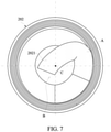
- FIG. 7 is a bottom view of a second end of a spring of the electrical connection assembly of the present disclosure.
- Numbering terms such as “first”, “second” or “third” can be used to describe various components, signals or the like, which are for distinguishing one component/signal from another one only, and are not intended to, nor should be construed to impose any substantive limitations on the components, signals or the like.
- FIG. 3 is an assembled view of an electrical connection assembly of the present disclosure.
- FIG. 4 is an exploded view of the electrical connection assembly of the present disclosure.
- FIG. 5 is an exploded cross-sectional view of the electrical connection assembly of the present disclosure.
- the electrical connection assembly 20 includes a main body 201 and a spring 202 .
- one end of the electrical connection assembly 20 is configured to be fixed onto a circuit board, and another end of the electrical connection assembly 20 is configured to be in contact with a device under test (e.g. each type of chips, sensors). Therefore, through the electrical connection assembly, related processors connected to the circuit board can determine a related electrical property state of the device under test in contact with the electrical connection assembly 20 .
- a device under test e.g. each type of chips, sensors
- the electrical connection assembly 20 of the present disclosure is configured to test an open/short state of electrical components.
- a plurality of the electrical connection assemblies 20 can be fixed in an electrical connection socket.
- the electrical connection socket is fixed onto the circuit board and is configured to carry a chip (e.g. memory chip), and the electrical connection assemblies 20 are configured to allow the chip disposed on the electrical connection socket and the circuit board to be electrically connected with each other. That is to say, the electrical connection assembly 20 of the present disclosure can be used as a probe of the electrical connection socket.
- the main body 201 is a conductive rod structure. As shown in FIG. 4 and FIG. 5 , two ends of the main body 201 are respectively defined as a contacting end 201 A and a tail end 201 B. The contacting end 201 A is configured to be in contact with the device under test.
- the main body 201 has a limiting protrusion 2011 (the limiting protrusion 2011 is an annular structure in FIG. 4 , but the present disclosure does not limit the structure of the limiting protrusion 2011 ) near the contacting end 201 A.
- the limiting protrusion 2011 divides the main body 201 into an exposed section 201 C and a concealed section 201 D that is surroundingly concealed by and within the main body 201 .
- An outer diameter D 1 of the limiting protrusion 2011 is greater than or equal to an outer diameter D 2 of the main body 201 within the exposed section 201 C.
- the outer diameter D 1 is greater than an outer diameter D 31 and an outer diameter D 32 of the main body 201 within the concealed section.
- the outer diameter D 1 of the limiting protrusion 2011 is greater than an outer diameter D 4 of the spring 202 .
- a fixing section 201 E of the main body 201 is divided from the concealed section 201 D, and the fixing section 201 E is near the limiting protrusion 2011 .
- the outer diameter D 31 of the main body 201 within the fixing section 201 E is greater than the outer diameter D 32 of the main body 201 within the concealed section 201 D excluding the fixing section 201 E.
- the main body 201 has the fixing section 201 E in the present embodiment, in a practical application, the main body 201 can be provided without the fixing section 201 E according to different assembling manners of the main body 201 and the spring 202 .
- the spring 202 is sleeved around the concealed section 201 D of the main body 201 , one end of the spring 202 is abutted against the limiting protrusion 2011 , and the spring 202 is limited by the limiting protrusion 2011 so that the spring 202 cannot leave the main body 201 from the contacting end 201 A of the main body 201 . That is to say, the spring 202 is not sleeved around the exposed section 201 C of the main body 201 .
- the spring has a first end 202 E 1 and a second end 202 E 2 respectively defined by two opposite ends of the spring 202 .
- the first end 202 E 1 of the spring 202 is correspondingly abutted against the limiting protrusion 2011 .
- the spring 202 is divided into a first tightly-coiled section 202 A, an elastic section 202 B, and a second tightly-coiled section 202 C sequentially from the first end 202 E 1 to the second end 202 E 2 .
- a pitch of the spring 202 within the first tightly-coiled section 202 A and a pitch of the spring 202 within the second tightly-coiled section 202 C are less than a pitch of the spring 202 within the elastic section 202 B.
- the pitch of the spring within the first tightly-coiled section 202 A or within the second tightly-coiled section 202 C can approach zero. That is to say, whether the spring 202 is pressed or not, the spring 202 does not deform within the first tightly-coiled section 202 A or the second tightly-coiled section 202 C.
- An inner diameter D 5 of the spring 202 within the first tightly-coiled section 202 A is less than the outer diameter D 31 of the main body 201 within the fixing section 201 E.
- the elastic section 202 B of the spring 202 When the spring sustains an external force, the elastic section 202 B of the spring 202 elastically deforms and correspondingly generates an elastic returning force, and when the spring 202 is no longer pressed, the elastic returning force allows the elastic section 202 B of the spring 202 to return to an initial position. That is to say, the elastic section 202 B of the spring 202 is mainly configured to provide the elastic returning force so that the spring 202 returns to the initial position.
- a length of the spring 202 within the first tightly-coiled section 202 A, a length of the spring 202 within the elastic section 202 B, and a length of the spring 202 within the second tightly-coiled section 202 C can be changed according to practical requirements, and FIG. 3 to FIG. 7 only show one of the embodiments of the present disclosure.
- An isodiametric section 202 C 1 and a tapered section 202 C 2 of the spring 202 are divided from the section tightly-coiled section 202 C.
- An outer diameter of the spring 202 within the isodiametric section 202 C 1 is uniform, and an outer diameter of the spring 202 within the tapered section 202 C gradually decreases.
- a minimum inner diameter D 6 of the spring 202 within the tapered section 202 C is less than the outer diameter D 32 of the main body 201 within the concealed section 201 D. That is to say, the outer diameter of the spring 202 of the present embodiment changes according to different positions within the tapered section 202 C, and the outer diameter of the spring 202 is basically uniform at positions excluding the tapered section 202 C.
- a difference L (as shown in FIG.
- the spring 202 elastically deforms after sustaining an external force, and when the spring 202 no longer deforms elastically from the external force, the tail end 201 B of the main body 201 is still correspondingly arranged inside of the spring 202 , and the tail end 201 B of the main body 201 does not penetrate through the spring 202 .
- a minimum outer diameter of the spring 202 within the tapered section 202 C 2 can be 0.6 to 0.8 of a maximum outer diameter of the spring 202 within any other section aside from the tapered section 202 C 2 .
- FIG. 6 is a cross-sectional view showing one end of the electrical connection assembly of the present disclosure being fixed on a circuit board
- FIG. 7 is a bottom view of a second end of a spring of the electrical connection assembly of the present disclosure.
- the electrical connection assembly 20 and a contacting portion S 1 of the circuit board S are fixed with each other.
- a length of the main body 201 along the axial direction i.e. the y-axis direction shown in FIG. 6 ) is less than the length of the spring 202 along the axial direction.
- the tail end 201 B of the main body 201 is correspondingly arranged inside of the spring 202 .
- the tail end 201 B of the main body 201 can be correspondingly arranged at the tapered section 202 C 2 or the isodiametric section 202 C 1 .
- the spring 202 is formed by a wire body spirally rotating relative to a central axis C, an end of the wire body bends toward the central axis C to form an end portion 2021 , and the end portion 2021 is arranged at a position of the second tightly-coiled section 202 C away from the first end 202 E 1 of the spring 202 .
- the end portion 2021 is configured to be mutually fixed with the contacting portion S 1 of the circuit board S. That is to say, the end portion 2021 that is configured to be mutually fixed with the contacting portion S 1 of the circuit board S is formed at an end of the second end 202 E 2 of the spring 202 .
- the end portion 2021 is formed by being bent toward the central axis C. Therefore, when the second end 202 E 2 of the spring 202 is in contact with the contacting portion S 1 of the circuit board S, a dot region A shown in FIG. 7 can be a region where the contacting portion S 1 of the circuit board S contacts.
- a dot region A shown in FIG. 7 can be a region where the contacting portion S 1 of the circuit board S contacts.
- the end portion 2021 of the spring 202 in the bottom view of one end of the end portion 2021 of the spring 202 , the end portion 2021 correspondingly passes through the central axis C, and the end portion 2021 extensively covers a hollow region B defined by the spring 202 surrounding the central axis C.
- the end portion 2021 of the spring 202 when the end portion 2021 of the spring 202 is fixed onto the contacting portion S 1 , the end portion 2021 can easily be in contact with the contacting portion S 1 , and an assembling speed of the electrical connection assembly 20 and the circuit board S can be effectively increased.
- the conventional electrical connection assembly contacts the contacting portion of the circuit board through the end surface of the contacting structure 1121 . Therefore, in a process where the end surface of the contacting structure 1121 is to contact the circuit board, it would be difficult for the contacting structure 1121 to correctly contact the contacting portion of the circuit board.
- the outer diameter of the spring 202 of the present disclosure is within a range of 0.05 mm to 3 mm. That is to say, the electrical connection assembly 20 is provided to improve on issues relating to the conventional electrical connection assembly having a small size.
Landscapes
- Physics & Mathematics (AREA)
- General Physics & Mathematics (AREA)
- Measuring Leads Or Probes (AREA)
Abstract
Description
Claims (6)
Applications Claiming Priority (2)
| Application Number | Priority Date | Filing Date | Title |
|---|---|---|---|
| TW108119126A TWI682179B (en) | 2019-06-03 | 2019-06-03 | Electrical connection assembly |
| TW108119126 | 2019-06-03 |
Publications (2)
| Publication Number | Publication Date |
|---|---|
| US20200379008A1 US20200379008A1 (en) | 2020-12-03 |
| US11226352B2 true US11226352B2 (en) | 2022-01-18 |
Family
ID=69942873
Family Applications (1)
| Application Number | Title | Priority Date | Filing Date |
|---|---|---|---|
| US16/823,434 Active 2040-03-26 US11226352B2 (en) | 2019-06-03 | 2020-03-19 | Electrical connection assembly |
Country Status (2)
| Country | Link |
|---|---|
| US (1) | US11226352B2 (en) |
| TW (1) | TWI682179B (en) |
Citations (6)
| Publication number | Priority date | Publication date | Assignee | Title |
|---|---|---|---|---|
| US4774462A (en) * | 1984-06-11 | 1988-09-27 | Black Thomas J | Automatic test system |
| US20150247882A1 (en) * | 2014-01-28 | 2015-09-03 | Mpi Corporation | Spring probe |
| US20150276807A1 (en) * | 2014-02-24 | 2015-10-01 | Mpi Corporation | Probe device having spring probe |
| US20170097376A1 (en) * | 2015-10-02 | 2017-04-06 | Mpi Corporation | Spring probe having outer sleeve and probe device having the same |
| US20170122978A1 (en) * | 2015-10-28 | 2017-05-04 | Mpi Corporation | Probe head |
| US20170192036A1 (en) * | 2015-12-31 | 2017-07-06 | Mpi Corporation | Probe structure and probe device |
Family Cites Families (5)
| Publication number | Priority date | Publication date | Assignee | Title |
|---|---|---|---|---|
| US20090066353A1 (en) * | 2007-08-29 | 2009-03-12 | Heetronix | Probe assemblies and methods for housing and providing electrical contact to planar or chip-type sensors and heaters |
| CN203535082U (en) * | 2013-10-29 | 2014-04-09 | 中芯国际集成电路制造(北京)有限公司 | Cantilever probe device |
| CN105044405B (en) * | 2015-08-26 | 2017-11-17 | 深圳市精实机电科技有限公司 | A kind of automatic capturing probe assembly |
| TWI608237B (en) * | 2016-05-09 | 2017-12-11 | Electrical connection device | |
| TWI592666B (en) * | 2016-09-12 | 2017-07-21 | 中華精測科技股份有限公司 | Slide probe |
-
2019
- 2019-06-03 TW TW108119126A patent/TWI682179B/en active
-
2020
- 2020-03-19 US US16/823,434 patent/US11226352B2/en active Active
Patent Citations (6)
| Publication number | Priority date | Publication date | Assignee | Title |
|---|---|---|---|---|
| US4774462A (en) * | 1984-06-11 | 1988-09-27 | Black Thomas J | Automatic test system |
| US20150247882A1 (en) * | 2014-01-28 | 2015-09-03 | Mpi Corporation | Spring probe |
| US20150276807A1 (en) * | 2014-02-24 | 2015-10-01 | Mpi Corporation | Probe device having spring probe |
| US20170097376A1 (en) * | 2015-10-02 | 2017-04-06 | Mpi Corporation | Spring probe having outer sleeve and probe device having the same |
| US20170122978A1 (en) * | 2015-10-28 | 2017-05-04 | Mpi Corporation | Probe head |
| US20170192036A1 (en) * | 2015-12-31 | 2017-07-06 | Mpi Corporation | Probe structure and probe device |
Also Published As
| Publication number | Publication date |
|---|---|
| TW202045929A (en) | 2020-12-16 |
| US20200379008A1 (en) | 2020-12-03 |
| TWI682179B (en) | 2020-01-11 |
Similar Documents
| Publication | Publication Date | Title |
|---|---|---|
| KR101936770B1 (en) | Contact device | |
| KR101894965B1 (en) | Probe pin and ic socket | |
| JP5133196B2 (en) | Probe connector | |
| US6053777A (en) | Coaxial contact assembly apparatus | |
| US20200233014A1 (en) | High speed probe card device and rectangular probe | |
| TWI706138B (en) | Probe | |
| EP2846415B1 (en) | Stepped spring contact | |
| JP4999079B2 (en) | probe | |
| JPH10261447A (en) | Contact piece provided with spring | |
| PH12014501745B1 (en) | Electrical connector with insulation member | |
| US20200028289A1 (en) | Pcie/sas connector structure | |
| JP2010539672A (en) | Spring contact assembly | |
| US5915995A (en) | Dual contact banana connector | |
| JP2011033410A (en) | Contact probe and socket | |
| US20230194570A1 (en) | Probe testing device having elastic structure | |
| KR102374774B1 (en) | Coaxial cable connector having window and coaxial connector apparatus using the coaxial cable connector | |
| US11226352B2 (en) | Electrical connection assembly | |
| KR102828069B1 (en) | Contact probe, probe holder and probe unit | |
| KR20150053480A (en) | Spring probe pin of inner bridge type having expanded tolerance | |
| US9429592B2 (en) | Connector | |
| US11437744B2 (en) | Printed circuit board assembly | |
| US11588266B2 (en) | Coaxial connector | |
| US4867709A (en) | Cinch plug | |
| US10658773B2 (en) | Deformable tubular contact with radial recess around contacting region | |
| US11394148B2 (en) | Contact probe and inspection socket provided with contact probe |
Legal Events
| Date | Code | Title | Description |
|---|---|---|---|
| AS | Assignment |
Owner name: C.C.P.CONTACT PROBES CO.,LTD., TAIWAN Free format text: ASSIGNMENT OF ASSIGNORS INTEREST;ASSIGNORS:WU, SHU-LIN;LIN, YEN-WEI;CHEN, WEI-CHU;AND OTHERS;SIGNING DATES FROM 20200302 TO 20200317;REEL/FRAME:052162/0884 |
|
| FEPP | Fee payment procedure |
Free format text: ENTITY STATUS SET TO UNDISCOUNTED (ORIGINAL EVENT CODE: BIG.); ENTITY STATUS OF PATENT OWNER: SMALL ENTITY |
|
| FEPP | Fee payment procedure |
Free format text: ENTITY STATUS SET TO SMALL (ORIGINAL EVENT CODE: SMAL); ENTITY STATUS OF PATENT OWNER: SMALL ENTITY |
|
| STPP | Information on status: patent application and granting procedure in general |
Free format text: DOCKETED NEW CASE - READY FOR EXAMINATION |
|
| STPP | Information on status: patent application and granting procedure in general |
Free format text: NON FINAL ACTION MAILED |
|
| STPP | Information on status: patent application and granting procedure in general |
Free format text: RESPONSE TO NON-FINAL OFFICE ACTION ENTERED AND FORWARDED TO EXAMINER |
|
| STPP | Information on status: patent application and granting procedure in general |
Free format text: NOTICE OF ALLOWANCE MAILED -- APPLICATION RECEIVED IN OFFICE OF PUBLICATIONS |
|
| STPP | Information on status: patent application and granting procedure in general |
Free format text: PUBLICATIONS -- ISSUE FEE PAYMENT RECEIVED |
|
| STPP | Information on status: patent application and granting procedure in general |
Free format text: PUBLICATIONS -- ISSUE FEE PAYMENT VERIFIED |
|
| STCF | Information on status: patent grant |
Free format text: PATENTED CASE |
|
| MAFP | Maintenance fee payment |
Free format text: PAYMENT OF MAINTENANCE FEE, 4TH YR, SMALL ENTITY (ORIGINAL EVENT CODE: M2551); ENTITY STATUS OF PATENT OWNER: SMALL ENTITY Year of fee payment: 4 |