US11225581B2 - Carbon nanotube aligned film as well as preparation method and application thereof - Google Patents
Carbon nanotube aligned film as well as preparation method and application thereof Download PDFInfo
- Publication number
- US11225581B2 US11225581B2 US17/271,603 US201817271603A US11225581B2 US 11225581 B2 US11225581 B2 US 11225581B2 US 201817271603 A US201817271603 A US 201817271603A US 11225581 B2 US11225581 B2 US 11225581B2
- Authority
- US
- United States
- Prior art keywords
- carbon nanotube
- dispersion solution
- polymer
- swcnts
- preparation
- Prior art date
- Legal status (The legal status is an assumption and is not a legal conclusion. Google has not performed a legal analysis and makes no representation as to the accuracy of the status listed.)
- Active
Links
- QKIJJOPILBXMPK-UTJRLIKCSA-N C.CC1=CC2=C(C(C)=C1)C(/N=N/C1=CC=CC=C1)=C(O)C=C2.CC1=CC2C(=O)C3=CC=CC=C3C(=O)C2C=C1O.[H]/N1=C2\C=C(N(C)C)C=C\C2=C\C2=CC=C(N(C)C)C=C21.[H]N1=C2C=C(N)C(C)=CC2=NC2=CC=C(N(C)C)C=C21.[H]N1=C2C=C(N)C=CC2=CC2=C1C=C(N)C=C2.[Y] Chemical compound C.CC1=CC2=C(C(C)=C1)C(/N=N/C1=CC=CC=C1)=C(O)C=C2.CC1=CC2C(=O)C3=CC=CC=C3C(=O)C2C=C1O.[H]/N1=C2\C=C(N(C)C)C=C\C2=C\C2=CC=C(N(C)C)C=C21.[H]N1=C2C=C(N)C(C)=CC2=NC2=CC=C(N(C)C)C=C21.[H]N1=C2C=C(N)C=CC2=CC2=C1C=C(N)C=C2.[Y] QKIJJOPILBXMPK-UTJRLIKCSA-N 0.000 description 2
- ANLBXZLFAMPFPB-UHFFFAOYSA-P B.C[N+](C)(C)CC(=O)C1=C2\C=C/C3=C/C=C\C4=C3C2=C(C=C4)/C=C\1.O=C1C2=CC=CC=C2C(=O)C2C(O)=C(O)C(S(=O)(=O)O[Na])=CC12.[Cl-].[Cl-].[H][N+]1=C2C=C(N(C)C)C=CC2=CC2=C/C=C(N(C)C)\C=C\21.[H][N+]1=C2C=C(N)C(C)=CC2=NC2=CC=C(CNC)C=C21.[H][N+]1=C2C=C(N)C=CC2=CC2=C1C=C(N)C=C2 Chemical compound B.C[N+](C)(C)CC(=O)C1=C2\C=C/C3=C/C=C\C4=C3C2=C(C=C4)/C=C\1.O=C1C2=CC=CC=C2C(=O)C2C(O)=C(O)C(S(=O)(=O)O[Na])=CC12.[Cl-].[Cl-].[H][N+]1=C2C=C(N(C)C)C=CC2=CC2=C/C=C(N(C)C)\C=C\21.[H][N+]1=C2C=C(N)C(C)=CC2=NC2=CC=C(CNC)C=C21.[H][N+]1=C2C=C(N)C=CC2=CC2=C1C=C(N)C=C2 ANLBXZLFAMPFPB-UHFFFAOYSA-P 0.000 description 1
- GJCRMDDXLDOEDE-WKWLGWBDSA-Q C.C.C=C(C[N+](C)(C)C)C1=C2\C=C/C3=C/C=C\C4=C3C2=C(C=C4)/C=C\1.CC1=CC2=CC=C(O)C(/N=N/C3=CC=CC=C3)=C2C([Na])=C1.CC1=CC2C(=O)C3=CC=CC=C3C(=O)C2C(O)=C1O.O=S(=O)=O.[Cl-].[H][N+]1=C2C=C(N(C)C)C=CC2=CC2=C/C=C(N(C)C)\C=C\21.[H][N+]1=C2C=C(N)C(C)=CC2=NC2=CC=C(CNC)C=C21.[H][N+]1=C2C=C(N)C=CC2=CC2=C1C=C(N)C=C2 Chemical compound C.C.C=C(C[N+](C)(C)C)C1=C2\C=C/C3=C/C=C\C4=C3C2=C(C=C4)/C=C\1.CC1=CC2=CC=C(O)C(/N=N/C3=CC=CC=C3)=C2C([Na])=C1.CC1=CC2C(=O)C3=CC=CC=C3C(=O)C2C(O)=C1O.O=S(=O)=O.[Cl-].[H][N+]1=C2C=C(N(C)C)C=CC2=CC2=C/C=C(N(C)C)\C=C\21.[H][N+]1=C2C=C(N)C(C)=CC2=NC2=CC=C(CNC)C=C21.[H][N+]1=C2C=C(N)C=CC2=CC2=C1C=C(N)C=C2 GJCRMDDXLDOEDE-WKWLGWBDSA-Q 0.000 description 1
- IDWWVQRFRMODEU-WKWLGWBDSA-Q C.C.CC1=CC2=CC=C(O)C(/N=N/C3=CC=CC=C3)=C2C([Na])=C1.CC1=CC2C(=O)C3=CC=CC=C3C(=O)C2C(O)=C1O.C[N+](C)(C)CC(=O)C1=C2\C=C/C3=C/C=C\C4=C3C2=C(C=C4)/C=C\1.O=S(=O)=O.[Cl-].[H][N+]1=C2C=C(N(C)C)C=CC2=CC2=C/C=C(N(C)C)\C=C\21.[H][N+]1=C2C=C(N)C(C)=CC2=NC2=CC=C(CNC)C=C21.[H][N+]1=C2C=C(N)C=CC2=CC2=C1C=C(N)C=C2 Chemical compound C.C.CC1=CC2=CC=C(O)C(/N=N/C3=CC=CC=C3)=C2C([Na])=C1.CC1=CC2C(=O)C3=CC=CC=C3C(=O)C2C(O)=C1O.C[N+](C)(C)CC(=O)C1=C2\C=C/C3=C/C=C\C4=C3C2=C(C=C4)/C=C\1.O=S(=O)=O.[Cl-].[H][N+]1=C2C=C(N(C)C)C=CC2=CC2=C/C=C(N(C)C)\C=C\21.[H][N+]1=C2C=C(N)C(C)=CC2=NC2=CC=C(CNC)C=C21.[H][N+]1=C2C=C(N)C=CC2=CC2=C1C=C(N)C=C2 IDWWVQRFRMODEU-WKWLGWBDSA-Q 0.000 description 1
- NUMUSJSWODBKML-SKORFANFSA-N CC1=CC2=C(C(C)=C1)C(/N=N/C1=CC=CC=C1)=C(O)C=C2.CC1=CC2C(=O)C3=CC=CC=C3C(=O)C2C=C1O.[H]/N1=C2\C=C(N(C)C)C=C\C2=C\C2=CC=C(N(C)C)C=C21.[H]N1=C2C=C(N)C(C)=CC2=NC2=CC=C(N(C)C)C=C21.[H]N1=C2C=C(N)C=CC2=CC2=C1C=C(N)C=C2.[Y] Chemical compound CC1=CC2=C(C(C)=C1)C(/N=N/C1=CC=CC=C1)=C(O)C=C2.CC1=CC2C(=O)C3=CC=CC=C3C(=O)C2C=C1O.[H]/N1=C2\C=C(N(C)C)C=C\C2=C\C2=CC=C(N(C)C)C=C21.[H]N1=C2C=C(N)C(C)=CC2=NC2=CC=C(N(C)C)C=C21.[H]N1=C2C=C(N)C=CC2=CC2=C1C=C(N)C=C2.[Y] NUMUSJSWODBKML-SKORFANFSA-N 0.000 description 1
- VLRBXMDXGXSOBB-GLCFPVLVSA-M O=S(=O)(O[Na])C1=CC2=CC=C(O)C(/N=N/C3=CC=CC=C3)=C2C([Na])=C1.O=S(=O)=O Chemical compound O=S(=O)(O[Na])C1=CC2=CC=C(O)C(/N=N/C3=CC=CC=C3)=C2C([Na])=C1.O=S(=O)=O VLRBXMDXGXSOBB-GLCFPVLVSA-M 0.000 description 1
Images


Classifications
-
- C—CHEMISTRY; METALLURGY
- C01—INORGANIC CHEMISTRY
- C01B—NON-METALLIC ELEMENTS; COMPOUNDS THEREOF; METALLOIDS OR COMPOUNDS THEREOF NOT COVERED BY SUBCLASS C01C
- C01B32/00—Carbon; Compounds thereof
- C01B32/15—Nano-sized carbon materials
- C01B32/158—Carbon nanotubes
- C01B32/168—After-treatment
- C01B32/174—Derivatisation; Solubilisation; Dispersion in solvents
-
- C—CHEMISTRY; METALLURGY
- C09—DYES; PAINTS; POLISHES; NATURAL RESINS; ADHESIVES; COMPOSITIONS NOT OTHERWISE PROVIDED FOR; APPLICATIONS OF MATERIALS NOT OTHERWISE PROVIDED FOR
- C09D—COATING COMPOSITIONS, e.g. PAINTS, VARNISHES OR LACQUERS; FILLING PASTES; CHEMICAL PAINT OR INK REMOVERS; INKS; CORRECTING FLUIDS; WOODSTAINS; PASTES OR SOLIDS FOR COLOURING OR PRINTING; USE OF MATERIALS THEREFOR
- C09D5/00—Coating compositions, e.g. paints, varnishes or lacquers, characterised by their physical nature or the effects produced; Filling pastes
- C09D5/24—Electrically-conducting paints
-
- C—CHEMISTRY; METALLURGY
- C01—INORGANIC CHEMISTRY
- C01B—NON-METALLIC ELEMENTS; COMPOUNDS THEREOF; METALLOIDS OR COMPOUNDS THEREOF NOT COVERED BY SUBCLASS C01C
- C01B32/00—Carbon; Compounds thereof
- C01B32/15—Nano-sized carbon materials
- C01B32/158—Carbon nanotubes
- C01B32/159—Carbon nanotubes single-walled
-
- C—CHEMISTRY; METALLURGY
- C01—INORGANIC CHEMISTRY
- C01B—NON-METALLIC ELEMENTS; COMPOUNDS THEREOF; METALLOIDS OR COMPOUNDS THEREOF NOT COVERED BY SUBCLASS C01C
- C01B32/00—Carbon; Compounds thereof
- C01B32/15—Nano-sized carbon materials
- C01B32/158—Carbon nanotubes
- C01B32/16—Preparation
-
- C—CHEMISTRY; METALLURGY
- C01—INORGANIC CHEMISTRY
- C01B—NON-METALLIC ELEMENTS; COMPOUNDS THEREOF; METALLOIDS OR COMPOUNDS THEREOF NOT COVERED BY SUBCLASS C01C
- C01B32/00—Carbon; Compounds thereof
- C01B32/15—Nano-sized carbon materials
- C01B32/158—Carbon nanotubes
- C01B32/168—After-treatment
-
- C—CHEMISTRY; METALLURGY
- C08—ORGANIC MACROMOLECULAR COMPOUNDS; THEIR PREPARATION OR CHEMICAL WORKING-UP; COMPOSITIONS BASED THEREON
- C08J—WORKING-UP; GENERAL PROCESSES OF COMPOUNDING; AFTER-TREATMENT NOT COVERED BY SUBCLASSES C08B, C08C, C08F, C08G or C08H
- C08J5/00—Manufacture of articles or shaped materials containing macromolecular substances
- C08J5/18—Manufacture of films or sheets
-
- C—CHEMISTRY; METALLURGY
- C08—ORGANIC MACROMOLECULAR COMPOUNDS; THEIR PREPARATION OR CHEMICAL WORKING-UP; COMPOSITIONS BASED THEREON
- C08K—Use of inorganic or non-macromolecular organic substances as compounding ingredients
- C08K3/00—Use of inorganic substances as compounding ingredients
- C08K3/02—Elements
- C08K3/04—Carbon
- C08K3/042—Graphene or derivatives, e.g. graphene oxides
-
- C—CHEMISTRY; METALLURGY
- C08—ORGANIC MACROMOLECULAR COMPOUNDS; THEIR PREPARATION OR CHEMICAL WORKING-UP; COMPOSITIONS BASED THEREON
- C08K—Use of inorganic or non-macromolecular organic substances as compounding ingredients
- C08K9/00—Use of pretreated ingredients
- C08K9/04—Ingredients treated with organic substances
-
- C—CHEMISTRY; METALLURGY
- C09—DYES; PAINTS; POLISHES; NATURAL RESINS; ADHESIVES; COMPOSITIONS NOT OTHERWISE PROVIDED FOR; APPLICATIONS OF MATERIALS NOT OTHERWISE PROVIDED FOR
- C09D—COATING COMPOSITIONS, e.g. PAINTS, VARNISHES OR LACQUERS; FILLING PASTES; CHEMICAL PAINT OR INK REMOVERS; INKS; CORRECTING FLUIDS; WOODSTAINS; PASTES OR SOLIDS FOR COLOURING OR PRINTING; USE OF MATERIALS THEREFOR
- C09D1/00—Coating compositions, e.g. paints, varnishes or lacquers, based on inorganic substances
-
- C—CHEMISTRY; METALLURGY
- C09—DYES; PAINTS; POLISHES; NATURAL RESINS; ADHESIVES; COMPOSITIONS NOT OTHERWISE PROVIDED FOR; APPLICATIONS OF MATERIALS NOT OTHERWISE PROVIDED FOR
- C09D—COATING COMPOSITIONS, e.g. PAINTS, VARNISHES OR LACQUERS; FILLING PASTES; CHEMICAL PAINT OR INK REMOVERS; INKS; CORRECTING FLUIDS; WOODSTAINS; PASTES OR SOLIDS FOR COLOURING OR PRINTING; USE OF MATERIALS THEREFOR
- C09D7/00—Features of coating compositions, not provided for in group C09D5/00; Processes for incorporating ingredients in coating compositions
- C09D7/20—Diluents or solvents
-
- C—CHEMISTRY; METALLURGY
- C09—DYES; PAINTS; POLISHES; NATURAL RESINS; ADHESIVES; COMPOSITIONS NOT OTHERWISE PROVIDED FOR; APPLICATIONS OF MATERIALS NOT OTHERWISE PROVIDED FOR
- C09D—COATING COMPOSITIONS, e.g. PAINTS, VARNISHES OR LACQUERS; FILLING PASTES; CHEMICAL PAINT OR INK REMOVERS; INKS; CORRECTING FLUIDS; WOODSTAINS; PASTES OR SOLIDS FOR COLOURING OR PRINTING; USE OF MATERIALS THEREFOR
- C09D7/00—Features of coating compositions, not provided for in group C09D5/00; Processes for incorporating ingredients in coating compositions
- C09D7/40—Additives
- C09D7/45—Anti-settling agents
-
- C—CHEMISTRY; METALLURGY
- C09—DYES; PAINTS; POLISHES; NATURAL RESINS; ADHESIVES; COMPOSITIONS NOT OTHERWISE PROVIDED FOR; APPLICATIONS OF MATERIALS NOT OTHERWISE PROVIDED FOR
- C09D—COATING COMPOSITIONS, e.g. PAINTS, VARNISHES OR LACQUERS; FILLING PASTES; CHEMICAL PAINT OR INK REMOVERS; INKS; CORRECTING FLUIDS; WOODSTAINS; PASTES OR SOLIDS FOR COLOURING OR PRINTING; USE OF MATERIALS THEREFOR
- C09D7/00—Features of coating compositions, not provided for in group C09D5/00; Processes for incorporating ingredients in coating compositions
- C09D7/40—Additives
- C09D7/60—Additives non-macromolecular
- C09D7/63—Additives non-macromolecular organic
-
- C—CHEMISTRY; METALLURGY
- C09—DYES; PAINTS; POLISHES; NATURAL RESINS; ADHESIVES; COMPOSITIONS NOT OTHERWISE PROVIDED FOR; APPLICATIONS OF MATERIALS NOT OTHERWISE PROVIDED FOR
- C09D—COATING COMPOSITIONS, e.g. PAINTS, VARNISHES OR LACQUERS; FILLING PASTES; CHEMICAL PAINT OR INK REMOVERS; INKS; CORRECTING FLUIDS; WOODSTAINS; PASTES OR SOLIDS FOR COLOURING OR PRINTING; USE OF MATERIALS THEREFOR
- C09D7/00—Features of coating compositions, not provided for in group C09D5/00; Processes for incorporating ingredients in coating compositions
- C09D7/40—Additives
- C09D7/65—Additives macromolecular
-
- H01L51/0048—
-
- H—ELECTRICITY
- H10—SEMICONDUCTOR DEVICES; ELECTRIC SOLID-STATE DEVICES NOT OTHERWISE PROVIDED FOR
- H10K—ORGANIC ELECTRIC SOLID-STATE DEVICES
- H10K71/00—Manufacture or treatment specially adapted for the organic devices covered by this subclass
- H10K71/10—Deposition of organic active material
- H10K71/12—Deposition of organic active material using liquid deposition, e.g. spin coating
- H10K71/15—Deposition of organic active material using liquid deposition, e.g. spin coating characterised by the solvent used
-
- H—ELECTRICITY
- H10—SEMICONDUCTOR DEVICES; ELECTRIC SOLID-STATE DEVICES NOT OTHERWISE PROVIDED FOR
- H10K—ORGANIC ELECTRIC SOLID-STATE DEVICES
- H10K85/00—Organic materials used in the body or electrodes of devices covered by this subclass
- H10K85/20—Carbon compounds, e.g. carbon nanotubes or fullerenes
- H10K85/221—Carbon nanotubes
- H10K85/225—Carbon nanotubes comprising substituents
-
- C—CHEMISTRY; METALLURGY
- C01—INORGANIC CHEMISTRY
- C01B—NON-METALLIC ELEMENTS; COMPOUNDS THEREOF; METALLOIDS OR COMPOUNDS THEREOF NOT COVERED BY SUBCLASS C01C
- C01B2202/00—Structure or properties of carbon nanotubes
- C01B2202/02—Single-walled nanotubes
-
- C—CHEMISTRY; METALLURGY
- C01—INORGANIC CHEMISTRY
- C01B—NON-METALLIC ELEMENTS; COMPOUNDS THEREOF; METALLOIDS OR COMPOUNDS THEREOF NOT COVERED BY SUBCLASS C01C
- C01B2202/00—Structure or properties of carbon nanotubes
- C01B2202/08—Aligned nanotubes
-
- C—CHEMISTRY; METALLURGY
- C01—INORGANIC CHEMISTRY
- C01B—NON-METALLIC ELEMENTS; COMPOUNDS THEREOF; METALLOIDS OR COMPOUNDS THEREOF NOT COVERED BY SUBCLASS C01C
- C01B2202/00—Structure or properties of carbon nanotubes
- C01B2202/20—Nanotubes characterized by their properties
- C01B2202/22—Electronic properties
-
- C—CHEMISTRY; METALLURGY
- C01—INORGANIC CHEMISTRY
- C01B—NON-METALLIC ELEMENTS; COMPOUNDS THEREOF; METALLOIDS OR COMPOUNDS THEREOF NOT COVERED BY SUBCLASS C01C
- C01B2202/00—Structure or properties of carbon nanotubes
- C01B2202/20—Nanotubes characterized by their properties
- C01B2202/28—Solid content in solvents
-
- C—CHEMISTRY; METALLURGY
- C01—INORGANIC CHEMISTRY
- C01B—NON-METALLIC ELEMENTS; COMPOUNDS THEREOF; METALLOIDS OR COMPOUNDS THEREOF NOT COVERED BY SUBCLASS C01C
- C01B2202/00—Structure or properties of carbon nanotubes
- C01B2202/20—Nanotubes characterized by their properties
- C01B2202/34—Length
-
- C—CHEMISTRY; METALLURGY
- C08—ORGANIC MACROMOLECULAR COMPOUNDS; THEIR PREPARATION OR CHEMICAL WORKING-UP; COMPOSITIONS BASED THEREON
- C08J—WORKING-UP; GENERAL PROCESSES OF COMPOUNDING; AFTER-TREATMENT NOT COVERED BY SUBCLASSES C08B, C08C, C08F, C08G or C08H
- C08J2365/00—Characterised by the use of macromolecular compounds obtained by reactions forming a carbon-to-carbon link in the main chain; Derivatives of such polymers
-
- C—CHEMISTRY; METALLURGY
- C08—ORGANIC MACROMOLECULAR COMPOUNDS; THEIR PREPARATION OR CHEMICAL WORKING-UP; COMPOSITIONS BASED THEREON
- C08K—Use of inorganic or non-macromolecular organic substances as compounding ingredients
- C08K3/00—Use of inorganic substances as compounding ingredients
- C08K3/02—Elements
- C08K3/04—Carbon
- C08K3/041—Carbon nanotubes
-
- Y—GENERAL TAGGING OF NEW TECHNOLOGICAL DEVELOPMENTS; GENERAL TAGGING OF CROSS-SECTIONAL TECHNOLOGIES SPANNING OVER SEVERAL SECTIONS OF THE IPC; TECHNICAL SUBJECTS COVERED BY FORMER USPC CROSS-REFERENCE ART COLLECTIONS [XRACs] AND DIGESTS
- Y02—TECHNOLOGIES OR APPLICATIONS FOR MITIGATION OR ADAPTATION AGAINST CLIMATE CHANGE
- Y02E—REDUCTION OF GREENHOUSE GAS [GHG] EMISSIONS, RELATED TO ENERGY GENERATION, TRANSMISSION OR DISTRIBUTION
- Y02E10/00—Energy generation through renewable energy sources
- Y02E10/50—Photovoltaic [PV] energy
- Y02E10/549—Organic PV cells
-
- Y—GENERAL TAGGING OF NEW TECHNOLOGICAL DEVELOPMENTS; GENERAL TAGGING OF CROSS-SECTIONAL TECHNOLOGIES SPANNING OVER SEVERAL SECTIONS OF THE IPC; TECHNICAL SUBJECTS COVERED BY FORMER USPC CROSS-REFERENCE ART COLLECTIONS [XRACs] AND DIGESTS
- Y02—TECHNOLOGIES OR APPLICATIONS FOR MITIGATION OR ADAPTATION AGAINST CLIMATE CHANGE
- Y02P—CLIMATE CHANGE MITIGATION TECHNOLOGIES IN THE PRODUCTION OR PROCESSING OF GOODS
- Y02P70/00—Climate change mitigation technologies in the production process for final industrial or consumer products
- Y02P70/50—Manufacturing or production processes characterised by the final manufactured product
Definitions
- the present application relates to a nano carbon material, particularly to a carbon nanotube aligned film as well as a preparation method and application thereof, belonging to the technical field of carbon nano materials.
- Carbon nanotubes have attracted much attentions from people due to their excellent mechanical property, optical property, electrical property and other properties, and are preliminarily applied in the fields of photoelectric devices, electronic devices, mechanical materials, conductive materials, composite materials and the like.
- CNTs are tubular nano materials and have extremely large aspect ratios and specific surface areas.
- there is a strong Van der Waal's force between CNTs so that CNTs are extremely easy to twine and agglomerate, and therefore CNTs are difficultly dispersed into a base and then the performances of the product are seriously restricted.
- the chemical modification method is that a strong acid is used as an oxidizing agent, an oxygenic functional group is formed on the tube wall or tail end of CNTs, CNTs are short cut into short CNTs of hundreds of meters, the functionalized CNTs can be effectively dispersed in aqueous solution and different organic solvents, a long-chain organic molecule is grafted utilizing a covalent bond so as to promote dispersity between CNTs, but the sp 2 structure and length of CNTs are destroyed in the process of surface modification, so as to lead to reduction in original property of CNTs, which is disadvantageous to application effect.
- the physical adsorption method is referred to as a non-covalent modification method in which an interface activator is used as the dispersing agent or a macromolecule (for example conjugated polymer) having a specific molecular structure binds to the surfaces of CNTs, thereby achieving the stable dispersion of carbon nanotubes in the dispersion medium.
- an interface activator is used as the dispersing agent or a macromolecule (for example conjugated polymer) having a specific molecular structure binds to the surfaces of CNTs, thereby achieving the stable dispersion of carbon nanotubes in the dispersion medium.
- a macromolecule for example conjugated polymer
- the main objective of the present application is to provide a carbon nanotube aligned film as well as a preparation method and application thereof, thereby overcoming the defects in the prior art.
- An embodiment of the present application provides a carbon nanotube dispersion solution, comprising:
- an organic solvent being at least used for cooperating with the rest components of the dispersion solution to form uniform dispersion solution.
- An embodiment of the present application also provides a preparation method of the above-mentioned carbon nanotube dispersion solution, comprising:
- An embodiment of the present application also provides a powder material, comprising:
- An embodiment of the present application also provides a preparation method of a carbon nanotube aligned film, comprising:
- an interface line between the water phase layer and the organic phase layer is close to a straight line.
- An embodiment of the present application also provides the carbon nanotube aligned film prepared by the above-mentioned method.
- the film is a continuously and uniformly aligned carbon nanotube film.
- An embodiment of the present application also provides use of the above-mentioned carbon nanotube aligned film in preparation of electronic devices, photoelectric devices, sensor devices or the like.
- An embodiment of the present application also provides an apparatus, comprising the above-mentioned carbon nanotube aligned film.
- the present application at least has the following beneficial effects:
- the preparation method of the carbon nanotube aligned film provided by the present application is to introduce the electrostatic repulsive force between tubes by adsorbing charged aromatic molecules on the surface of the conjugated polymer molecule dispersed high-pure carbon nanotube molecule to resist close packing and twining phenomena brought by densification and rearrangement in the process of inducing alignment by the external force;
- the present application utilizes a double-liquid layer impregnation pulling method to perform alignment on the above high-pure carbon nanotubes, the water phase layer plays a certain liquid seal role in the organic phase on the lower layer, slows down the volatilization speed of the organic phase so as to prolong the self-assembling time of the carbon nanotubes in a meniscus at an air-organic phase interface and achieves the rearrangement and ordered arrangement of the carbon nanotubes at the air-organic phase interface line, thereby obtaining the carbon nanotube aligned film that is in consistency arrangement along the pulling direction;
- the preparation method of the present application is not only simple and efficient, but also is easily used for scale-up preparation of the large-area alignment carbon nanotube film, and provides a firm material safeguard for application of the carbon nanotube films in the field of electronic devices.
- FIG. 1 is a flowchart of a preparation process of a high-pure semiconductor type single-walled carbon nanotube, which is used for introducing an electrostatic repulsive force between tubes and preparing a large-area continuous aligned carbon nanotube film according to a typical embodiment of the present application;
- FIG. 2 is a process diagram of a double-liquid layer impregnation pulling method for preparing a large-area continuous aligned CNTs film according to a typical embodiment of the present application;
- FIG. 3A is a SEM image of high-pure semiconductor type single-walled carbon nanotube aligned films obtained according to a typical embodiment 1 of the present application;
- FIG. 3B is a SEM image of high-pure semiconductor type single-walled carbon nanotube aligned films obtained according to a typical embodiment 2 of the present application;
- FIG. 3C is a SEM image of high-pure semiconductor type single-walled carbon nanotube aligned films obtained according to a typical embodiment 3 of the present application;
- FIG. 3D is a SEM image of high-pure semiconductor type single-walled carbon nanotube aligned films obtained according to a typical embodiment 4 of the present application;
- FIG. 3E is a SEM image of high-pure semiconductor type single-walled carbon nanotube aligned films obtained according to a typical embodiment 5 of the present application;
- FIG. 3F is a SEM image of high-pure semiconductor type single-walled carbon nanotube aligned films obtained according to a typical embodiment 6 of the present application;
- FIG. 3G is a SEM image of high-pure semiconductor type single-walled carbon nanotube aligned films obtained according to a typical embodiment 7 of the present application;
- FIG. 3H is a SEM image of high-pure semiconductor type single-walled carbon nanotube aligned films obtained according to a typical embodiment 8 of the present application;
- FIG. 3I is a SEM image of high-pure semiconductor type single-walled carbon nanotube aligned films obtained according to a typical embodiment 9 of the present application;
- FIG. 4A is a diagram showing fluorescent curve change after different PFS aromatic molecules are adsorbed on the surface of a conjugated polymer dispersed high-pure semiconductor type single-walled carbon nanotube according to a typical embodiment 1 of the present application;
- FIG. 4B is a diagram showing fluorescent curve change after different PFS aromatic molecules are adsorbed on the surface of a conjugated polymer dispersed high-pure semiconductor type single-walled carbon nanotube according to a typical embodiment 2 of the present application;
- FIG. 5A is a polarization Raman spectrum indicating the alignment of a semiconductor type single-walled carbon nanotube film according to a typical embodiment 6 of the present application, which characterize alignment;
- FIG. 5B is a polarization Raman spectrum indicating the alignment of a semiconductor type single-walled carbon nanotube film according to a typical embodiment 6 of the present application, which characterize alignment.
- One aspect of the embodiment of the present application provides a dispersion solution of a carbon nanotube, comprising:
- a polymer as a carbon nanotube dispersing agent, specifically binding to the selected carbon nanotube;
- an organic solvent being at least used for cooperating with the dispersion solution to form a uniform dispersion solution.
- the “selected carbon nanotube” corresponds to the “polymer”, for example polyvinylpyrrolidone, high-branched polymers and aniline oligomers.
- the “selected carbon nanotube” can be a single-walled carbon nanotube, a few-walled carbon nanotube, a multi-walled carbon nanotube and the like.
- the “selected carbon nanotube” can be a semiconductor type single-walled carbon nanotube.
- the polymer can be used as the carbon nanotube dispersing agent to separate at least a part of a plurality of carbon nanotubes into their individual sizes (0.4-100 nm in diameter), and stably disperse them into a dispersion medium such as an organic solvent in the state of “isolated dispersion” (without condensation).
- a dispersion medium such as an organic solvent in the state of “isolated dispersion” (without condensation).
- isolated dispersion” in the present application refers to a state that carbon nanotubes do not become a bulk form, a recommendationform and a rope form due to mutual cohesive force, which are dispersed into the dispersion medium in isolation one by one.
- different polymers can be respectively selected as dispersing agents of different types of carbon nanotubes.
- polyvinylpyrrolidone for single-walled carbon nanotubes, double-walled carbon nanotubes and multi-walled carbon nanotubes, polyvinylpyrrolidone, highly branched polymers having a triarylamine structure as a branching point, ananiline oligomers and derivatives thereof can be used as corresponding carbon nanotube dispersing agents.
- polyvinylpyrrolidone highly branched polymers having a triarylamine structure as a branching point
- ananiline oligomers and derivatives thereof can be used as corresponding carbon nanotube dispersing agents.
- documents such as JP200044216A, JP2005162877A, JP200824522A, WO2008/139839A, CN102695557B, CN101578237B, CN105645388B, CN105645387A, CN105642184B and CN106061894A for single-walled carbon nanotubes, double-walled carbon nanotubes and
- suitable polymers as carbon nanotube dispersing agents can be conjugated homopolymers or homopolymers based on carbazolyl, fluorenyl and thienyl, such as polythiophene derivatives, polyfluorene and/or polyfluorene derivatives and poly(m-phenylacetylene) derivatives, and polymers with other structures, such as tree-shaped conjugated polymers. More specifically, polycarbazole, polyfluorene, polythiophene, carbazole linear copolymers (PCz) and the like are especially suitably used as dispersing agents for semiconductor type single-walled carbon nanotubes.
- PCz carbazole linear copolymers
- These polymers can specifically bind to semiconductor type single-walled carbon nanotubes through physical action such as ⁇ - ⁇ interaction, and promote the stable “isolated dispersion” of semiconductor type single-walled carbon nanotubes in organic solvents and other dispersion media. More further, for selection of these polymers, please refer to CN103112840B, CN105585000B, CN107456918A, CN106823983A, CN106478927A, CN105611986B, etc.
- the aromatic molecule can bind to the carbon nanotube whose surface specifically binds to the polymer and allow the surfaces of various carbon nanotubes in the same dispersion system to have the same charges (positive charges or negative charges), thereby forming an electrostatic repulsive force between various carbon nanotubes to resist close packing and twining phenomena brought by densification and rearrangement in the process of inducing alignment by the external force.
- the selected carbon nanotube is the semiconductor type single-walled carbon nanotube
- the carbon nanotube dispersing agent adaptive to the carbon nanotube can be a conjugated polymer such as a conjugated homopolymer or homopolymer based on carbazyl, fluorenyl and thienyl, especially for example can be a homopolymer or copolymer selected from at least one of carbazole, polyfluorene, polythiophene, polyhenylene and the like
- the copolymerization unit of the copolymer comprises any one of benzene, thiophene, pyridine, triarylamine and benzothiadiazole or alkylated derivatives thereof or combinations thereof, and preferably is selected from carbazole linear copolymer (PCz) and the like, but is not limited thereto.
- the aromatic molecule preferably has a condensed ring aromatic conjugated structure (which can interact with the semiconductor type single-walled carbon nanotube through ⁇ - ⁇ stacking interaction) and atoms or substituents (which are used for introducing electrostatic repulsive force between tubes in order to charge the surface of the semiconductor type single-walled carbon nanotube) with positive charges or negative charges.
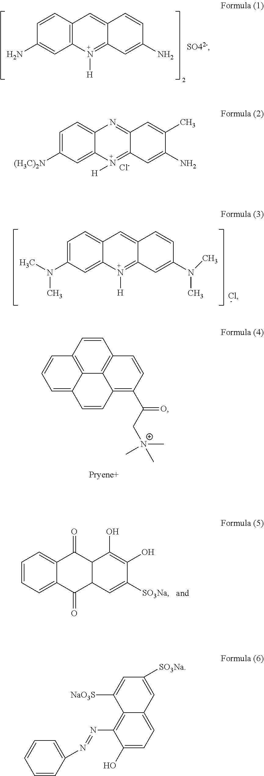
- the structural formula of the aromatic molecule comprises at least one of formula (I)-formula (V):
- X comprises SO 4 2 ⁇ , SO 3 2 ⁇ , CO 3 2 ⁇ , NO 3 ⁇ or Cl ⁇
- Y comprises Cl
- Z comprises Na + or K + .
- the typical structure of the aromatic molecule can refer to any compound of the following formulas (1)-(6), but is not limited thereto.
- a dye aromatic small molecule with positive charges is used as a preferred embodiment, that is, Proflavine Hemisufate (PFS) molecule of formula (I).
- PFS Proflavine Hemisufate
- s-SWCNTs semiconductor type single-walled carbon nanotubes
- These-mentioned semiconductor type single-walled carbon nanotubes have unique structures and electronic features, such as over-length diameter ratios, large specific areas and adjustable band gaps, excellent electron and hole mobility (this carrier mobility is up to 70000 cm 2 V ⁇ 1 s ⁇ 1 ), is considered as one of the most promising materials that are used for preparing next-generation field effect films and radio frequency transistors.
- One-dimensional characteristic of a single s-SWCNTs makes it exhibit extremely significant anisotropy in the aspects of electrical, optical, mechanical, magnetic and other properties.
- the s-SWCNTs solution obtained based on a solution method can be used for preparing large-area out-of-order network-like carbon nanotube films through different methods.
- the carbon nanotubes randomly distributed in the network-like carbon nanotube film have obvious twining and overlapping phenomena, the migration rate of the carriers is reduced to a great extent due to increase in contact resistor between tubes, which cannot exert the excellent performance of the single carbon nanotube and is disadvantageous to achievement of high-performance integrated circuits.
- one of main solution ideas is to prepare a large-area aligned s-SWCNTs film.
- There are mainly two methods for achieving alignment of carbon nanotubes one method is that an aligned array of carbon nanotubes is directly grown via chemical vapor deposition, and the other method is alignment of the carbon nanotubes pre-separated in the solution.
- a mixture of metal type and semiconductor type carbon nanotubes is obtained through the direct growth method, the existence of the metal type single-walled carbon nanotubes seriously affects the performances of carbon nanotube film transistor devices. Therefore, it is necessary to further optimize the purity of the directly grown semiconductor type carbon nanotubes.
- CN107963610A discloses that the precise control of positions, alignment density and patterning of the alignment carbon nanotube film is achieved by using ink jet printing on the functionalized hydrophobic base, and carbon nanotube films having uniform density, consistent alignment and different patterns are arranged.
- this method is only suitable for alignment of carbon nanotubes in a surfactant system, which cannot get rid of inherent defects of alignment technology of s-SWCNTs in the surfactant system.
- the purity of s-SWCNTs dispersed by surfactants is not high enough; on the other hand, the surface of s-SWCNTs is coated with excessive residual surfactants, which seriously hinders the transfer of charges and significantly reduces the performance of the device.
- CN106061894A discloses that the s-SWCNTs film is deposited through the organic dispersion solution of s-SWCNTs dispersed by polyfluorene derivatives, The thin layer of the organic dispersion solution of s-SWCNTs spreads on the surface of the aqueous medium to induce evaporation self-assembling when contacting with the solid base.
- the high density film of the semiconductor type single-walled carbon nanotube with a certain degree of alignment is prepared by this method.
- the polyfluorene derivatives used in this technology are electrically neutral molecules without charges, and the s-SWCNTs can be twined and overlapped with each other due to van Der Waal's force.
- s-SWCNTs In the process of inducing alignment under the action of external force, s-SWCNTs often inevitably generate twining and close packing phenomena in the process of rearrangement and densification, which is unfavorable for the alignment of s-SWCNTs.
- the large-area uniform s-SWCNTs film can be obtained through rapid evaporation of the organic solvent in the process of pulling the base from the s-SWCNTs suspension, thereby realizing rapid and controllable preparation of high-quality, large-area and high-uniformity s-SWCNTs films.
- one common problem of these existing technologies is that alignment of s-SWCNTs cannot be well realized.
- a kind of charged aromatic molecules are adopted to be adsorbed to the surface of the separated high-pure semiconductor type single-walled carbon nanotube such as a conjugated polymer molecule in the organic system through ⁇ - ⁇ stacking interaction so that the surface of the semiconductor type single-walled carbon nanotube is charged so as to introduce the electrostatic repulsive force between tubes, thereby obtaining the dispersion solution of the high-pure semiconductor type single-walled nanotube with trace repulsive force introduced between semiconductor type single-walled nanotubes and good stability.
- the introduced electrostatic repulsive force between tubes is used to resist the twining and close packing brought by the self-assembling process during the alignment, and then promote the efficient, uniform and large-area alignment of s-SWCNTs.
- a mass ratio of carbon nanotubes to the polymer in the dispersion solution is 1:0.001-1:100, preferably 1:0.01-1:50, particularly preferably 1:0.1-1:10.
- a mass ratio of carbon nanotubes to the aromatic molecules in the dispersion solution is 1:0.005-1:50, preferably 1:0.05-1:20, particularly preferably 1:0.1-1:10.
- the content of the carbon nanotubes in the dispersion solution is 0.5 ⁇ g/mL or more.
- the average length of the carbon nanotubes in the dispersion solution is 100-3000 nm.
- the organic solvent comprises a combination of any one or more than two of haloalkane, aromatic hydrocarbon, aryl halide and the like, but is not limited thereto.
- the haloalkane can be selected from a combination of any one or more than two of chloroform, dichloromethane, dichloroethane and the like, the aromatic hydrocarbon can be selected from toluene, xylene and the like, and the aryl halide can be selected from chlorobenzene, dichlorobenzene and the like but is not limited thereto.
- Another aspect of the embodiment of the present application also provides a preparation method of the above-mentioned carbon nanotube dispersion solution, comprising:
- the preparation method can specifically comprises:
- the single-walled carbon nanotube powder raw material is selected from original single-walled carbon nanotubes, and is prepared by an arc discharge method, a plasma discharge method, a laser ablation method or a chemical vapor deposition method but not limited thereto.
- the preparation method comprises: mixing and ultrasonically dispersing the conjugated polymer and the original single-walled carbon nanotube, and then filtering and washing to remove the conjugated polymer molecule coating on the surface of the semiconductor type single-walled carbon nanotube to obtain a semiconductor type single-walled carbon nanotube with the purity of 99.9% or more.
- the preparation method can comprise: selectively dispersing the semiconductor type single-walled carbon nanotube with the purity of 99.9% utilizing the conjugated polymer in the organic system, then filtering in vacuum and washing to obtain the semiconductor type single-walled carbon nanotube powder with a small amount of conjugated polymer remained on the surface and good monodispersity, further purifying the high-pure semiconductor type single-walled carbon nanotube while ensuring that the washed semiconductor type single-walled carbon nanotube can realize monodispersion again.
- a preparation method of a semiconductor type single-walled carbon nanotube dispersion solution can comprise the following steps:
- a certain mass of conjugated polymer and original single-walled carbon nanotubes are accurately weighed and mixed in a certain volume of xylene (or toluene) solvent, the polymer is ultrasonically and sufficiently dissolved in a water bath, then subjected to ultrasonic dispersion using an ultrasonic pulverizer.
- the dispersed carbon nanotube solution is pre-separated at a rotation low speed to obtain a supernatant, and then centrifuged at a high rotation speed to obtain a supernatant, namely, the xylene (or toluene) dispersion solution of the high-pure semiconductor type single-walled carbon nanotube whose surface is coated with excessive polymer molecules.
- the xylene (or toluene) dispersion solution of the high-pure semiconductor type single-walled carbon nanotube whose surface is coated with excessive polymer molecules obtained in step 1) is poured into a funnel for vacuum filtration.
- the separated high-pure semiconductor type single-walled carbon nanotube solid is left on a filter film, and then the filter film is washed with a large amount of organic solvents (tetrahydrofuran, chloroform, dichloromethane, etc.) to remove the excessive polymer molecules coating on the surface of the semiconductor type single-walled carbon nanotube to obtain the semiconductor type single-walled carbon nanotube solid powder (that is, the first powder) with a small amount of polymer molecules.
- the preparation method specifically can comprise: re-dispersing the above obtained semiconductor type single-walled carbon nanotube solid powder into the organic solution of condensed ring aromatic small molecules to obtain the organic dispersion solution of the high-pure semiconductor type single-walled carbon nanotube with electrostatic repulsive force introduced between tubes.
- the preparation method also comprises: filtering the chloroform dispersion solution of the high-pure semiconductor type single-walled carbon nanotubes with electrostatic repulsive force introduced between tubes in vacuum so that the semiconductor type single-walled carbon nanotube solid with the electrostatic repulsive force introduced on the surface is left on the filter film, then washing the filter film using a large amount of organic solvent to remove the free condensed ring aromatic small molecules until the filtrate has no absorption peak of this molecule and finally the high-pure semiconductor type single-walled carbon nanotube solid powder (that is, the second powder) with electrostatic repulsive force introduced between tubes and without free condensed ring aromatic molecules is obtained, and re-dispersing the solid powder into the organic solvent to obtain the dispersion solution of the high-pure semiconductor type single-walled carbon nanotube with electrostatic repulsive force introduced between tubes and without free condensed ring aromatic small molecules.
- Another aspect of the embodiment of the present application also provides a powder material, comprising:
- the aromatic molecule preferably has a condensed ring aromatic conjugated structure (which is used for interacting with the semiconductor type single-walled carbon nanotube through ⁇ - ⁇ stacking interaction) and atoms or substituents (which is used for charging the surface of the semiconductor type single-walled carbon nanotube to introduce the electrostatic repulsive force between tubes) with positive charges or negative charges
- the structural formula includes at least one of formula (I)-formula (V), and the typical structure can refer to any one compound of formula (1)-(6), but is not limited thereto.
- one of the dye aromatic small molecules with positive charges serves as a preferred embodiment, that is, a Proflavine Hemisufate (PFS) molecule of formula (1).
- PFS Proflavine Hemisufate
- the conjugated polymer is a conjugated homopolymer or homopolymer based on carbazolyl, fluorenyl and thienyl, such as a homopolymer or copolymer of at least one of polycarbazole, polyfluorene, polythiophene and polyphenylene ethylene, wherein the copolymerization unit of the copolymer is selected from any one of benzene, thiophene, pyridine, triarylamine and benzothiadiazole or alkylated derivatives thereof or a combination thereof.
- the conjugated polymer is preferably selected from a carbazole linear copolymer (PCz), but is not limited to thereto.
- the conjugated polymer can also be replaced as a benzobenzene small molecule dispersing agent, please refer to CN107298436A.
- the mass ratio of carbon nanotubes to a polymer in the powder material is 1:0.001-1:100, preferably 1:0.01-1:50, particularly preferably 1:0.1-1:10.
- the mass ratio of carbon nanotubes to aromatic molecules in the powder material is 1:0.005-1:50, preferably 1:0.05-1:20, particularly preferably 1:0.1-1:10.
- the average length of the semiconductor type single-walled carbon nanotubes in the powder material is 100-3000 nm.
- Another aspect of the embodiment of the present application also provides a preparation method of a semiconductor type single-walled carbon nanotube aligned film, comprising:
- the preparation method specifically comprises: disposing the water phase layer on the dispersion solution of the carbon nanotubes, and then pulling out the base from the dispersion solution of the carbon nanotube via a two-phase interface of the water phase layer and the organic phase layer using a double-liquid layer impregnation pulling method to obtain the carbon nanotube film, thereby obtaining the carbon nanotube aligned film being in consistency arrangement along the pulling direction.
- the water phase layer plays a liquid seal role in the organic phase on the lower layer, which can slow down the volatilization rate of the organic phase, prolong the self-assembling time of carbon nanotubes in the meniscus at the air-organic phase interface, and realize the rearrangement and ordered arrangement of carbon nanotubes at the air-organic phase interface line.
- the carbon nanotube aligned film is deposited by utilizing the organic phase where carbon nanotubes with electrostatic repulsive force between tubes are dissolved.
- the water phase layer with a certain thickness is added on the organic phase where carbon nanotubes with electrostatic repulsive force between tubes are dissolved, and the solid base is pulled out from the organic phase through the organic phase-water phase interface.
- the interface line between the water phase layer and the organic phase layer in the double-layer liquid phase system is close to a straight line.
- the preparation method comprises: inserting the base into the double-layer liquid phase system at a descent rate of 200-2000 ⁇ m/s (preferably 500-1500 ⁇ m/s, particularly preferably 800-1000 ⁇ m/s).
- the preparation method further comprises immersing most of the base into the dispersion solution of the carbon nanotubes.
- the preparation method can comprise: pulling out the base from the double-layer liquid phase system at an upward pulling speed. This process goes through the water-organic phase interface line and prolongs the self-assembling time of the semiconductor type single-walled carbon nanotube in the meniscus at the air-organic phase interface under the action of liquid seal applied by the water phase layer, so as to realize the rearrangement and ordered arrangement of the carbon nanotubes.
- the upward pulling speed of the base includes a slow pulling speed and a rapid pulling speed.
- the preparation method can comprise: pulling out the base from the double-layer liquid phase system at a pulling rate of 1-5000 ⁇ m/s, preferably 50-1000 ⁇ m/s, more preferably 200-500 ⁇ m/s.
- the water phase layer comprises pure water or aqueous solution.
- the aqueous solution can also comprise inorganic salts, organic solvents and the like, which are at least used for adjusting the viscosity and tension of the double-layer liquid phase system.
- the thickness of the water phase layer is 1-15 mm.
- the base has a hydrophobic surface.
- the material of the base can be a rigid material, a flexible material and the like, the rigid material comprises silicon oxide wafer, quartz wafer, sapphire substrate and the like, and the flexible material comprises polyethylene naphthalate (PEN), polyethylene terephthalate (PET), polyimide (PI) and the like, but is not limited to thereto.
- PEN polyethylene naphthalate
- PET polyethylene terephthalate
- PI polyimide
- Another aspect of the embodiment of the present application also provides a carbon nanotube aligned film prepared by the above method.
- the film comprises a plurality of aligned carbon nanotubes, and is a continuously and uniformly aligned carbon nanotube film.
- the thickness of the film is 2-5 nm.
- the edge region of the base surface is removed, and large-area continuously and uniformly aligned carbon nanotubes can be realized in the effective film-forming region of the base surface.
- the alignment direction of the carbon nanotubes is consistent with the pulling direction.
- Another aspect of the embodiment of the present application also provides use of the above semiconductor type single-walled carbon nanotube aligned film in the fields of electronic devices, photoelectric devices, sensor devices and the like.
- Another aspect of the embodiment of the present application also provides an apparatus, comprising the above semiconductor type single-walled carbon nanotube aligned film.
- the apparatus can be an electronic device such as a thin film transistor, a field effect transistor, a memory and an integrated circuit device, or a photoelectric device such as a photovoltaic device and a photodetector, or any one of sensor devices such as a chemical sensor and a biosensor, but is not limited to thereto.
- an electronic device such as a thin film transistor, a field effect transistor, a memory and an integrated circuit device, or a photoelectric device such as a photovoltaic device and a photodetector, or any one of sensor devices such as a chemical sensor and a biosensor, but is not limited to thereto.
- the preparation method of the present application is not only simple and efficient, but also can effectively solve the problems existing in the prior art, such as carbon nanotube purity, twining and packing of carbon nanotubes in the process of inducing alignment by external force, and small effective carbon nanotube alignment area.
- the preparation method of the present application is not only simple and efficient, but also easy to scale up and prepare large-area continuous aligned carbon nanotube film, which provides a solid material guarantee for the application in the field of electronic devices based on carbon nanotube films.
- s-SWCNTs dispersion solution, powder and aligned film
- FIG. 1 a preparation method of dispersion solution, powder and aligned film (hereinafter referred to as s-SWCNTs) of a semiconductor type single-walled carbon nanotube, as shown in FIG. 1 , which can specifically comprises the following general steps:
- a certain mass of conjugated polymer and original single-walled carbon nanotubes are accurately weighed and mixed in an organic solvent, and the polymer is sufficiently and ultrasonically dissolved in a water bath and then subjected to ultrasonic dispersion using an ultrasonic pulverizer.
- the dispersed carbon nanotube solution is pre-separated at a low rotation speed to obtain a supernatant, and then centrifuged at a high rotation speed to obtain a supernatant, namely, the dispersion solution of high-pure s-SWCNTs whose surface is coated with excessive polymer molecules, which is dispersed and extracted by the polymer.
- the dispersion solution of the s-SWCNTs whose surface is coated with excessive polymer molecules obtained in step 1) is poured into a funnel for vacuum filtration.
- the separated high-pure semiconductor type single-walled solid is left on a filter film, and then the filter film is washed with a large amount of solvents to remove excessive polymer molecules coating on the surface of the s-SWCNTs to obtain the s-SWCNTs solid powder (that is, the first powder) with a small amount of polymer molecules left on the surface.
- the s-SWCNTs solid powder obtained in step 1.2 is re-dispersed into the organic solution of the aromatic molecule to obtain the high-pure s-SWCNTs dispersion solution with electrostatic repulsive force introduced between tubes.
- step 1.3 the high-pure s-SWCNTs dispersion solution with electrostatic repulsive force introduced between tubes is filtered in vacuum, the s-SWCNTs solid with electrostatic repulsive force introduced on the surface is left on the filter film, the filter film is washed with a large amount of solvent to remove the free aromatic molecules until the filtrate has no absorption peak of the aromatic molecule. Finally, the high-pure s-SWCNTs solid powder (i.e., second powder) with electrostatic repulsive force introduced between tubes and without free aromatic molecules is obtained.
- the s-SWCNTs solid powder obtained in step 1.4 is re-dispersed into the organic solvent to obtain the dispersion solution of the high-pure s-SWCNTs with electrostatic repulsive force introduced between tubes and without free aromatic molecules is obtained.
- the preparation method of the semiconductor type single-walled carbon nanotube aligned film especially comprises the following operation steps:
- a certain volume of organic dispersion solution of s-SWCNTs obtained in step 1.5 is added into a square quartz colorimetric dish with organic corrosion resistance. Then a certain volume of deionized water is added on the upper layer of the dispersion solution to form a water phase layer having a certain thickness and meanwhile ensure that the two-phase interface line between the water phase layer and the organic layer is basically close to a straight line. Thus, a double-liquid layer with a stable liquid-liquid two-phase interface line is formed.
- the hydrophobic base is inserted into the organic dispersion solution of s-SWCNTs via the water phase layer on the upper layer at a certain descent speed (namely v 1 ), and most of the hydrophobic base is immersed into the organic dispersion solution of s-SWCNTs.
- the hydrophobic base is pulled out from the organic dispersion solution where the high-pure s-SWCNTs with repulsive force introduced between tubes are dissolved at a certain upward pulling speed (i.e., v 2 ).
- This process can go through the water-organic interface line and prolong the self-assembling time of s-SWCNTs in the meniscus at the air-organic phase interface under the action of liquid seal applied by the water phase layer, thereby realizing the rearrangement and ordered arrangement of s-SWCNTs.
- step 1.1 On the basis of general step 1.1, referring to CN108017049A, a feed ratio of a carbazole linear copolymer (PCz) to a single-walled carbon nanotube raw material (commercially available and made by an arc discharge method) was adjusted to 1:1 (mass ratio, if not specified), and toluene was used as a dispersing agent.
- the toluene dispersion solution of polymer-dispersed high-pure s-SWCNTs was obtained by ultrasonic dispersion and centrifugation.
- step 2) The first powder obtained in step 2) was re-dispersed into chloroform solution of Proflavine Hemisufate (PFS) with a mass concentration of 0.02 mg/mL, and chloroform dispersion solution of high-pure s-SWCNTs with electrostatic repulsive force introduced between tubes was obtained.
- PFS Proflavine Hemisufate
- the second powder obtained in step 4) was re-dispersed into a chloroform solvent to obtain chloroform dispersion solution of high-pure s-SWCNTs with electrostatic repulsive force introduced between tubes and without free Proflavine Hemisufate (PFS) molecules.
- the content of s-SWCNTs was 0.5 ⁇ g/mL or more, and the average length of s-SWCNTs was 100-3000 nm,
- the mass ratio of s-SWCNTs to conjugated polymer was 1:0.001
- the mass ratio of s-SWCNTs to Proflavine Hemisufate (PFS) molecules was 1:0.005.
- Proflavine Hemisufate (PFS) molecule itself, as a fluorescent dye molecule, was adsorbed onto the surface of high-pure s-SWCNTs through ⁇ - ⁇ stacking, its fluorescence can be quenched by s-SWCNTs, and correspondingly the fluorescence intensity was significantly reduced, as shown in FIG. 4A .
- the concentration of chloroform dispersion solution used for pulling was 5 ⁇ g/mL. Then deionized water was added onto the upper layer of the dispersion solution to form a water phase layer with a thickness of 1 mm. The silicon oxide wafer was inserted into chloroform dispersion solution at a descent rate (v 1 ) of 1000 ⁇ m/s, and then pulled out at an upward pulling rate (v 2 ) of 200 ⁇ m/s.
- FIG. 3A the SEM image of the semiconductor type single-walled carbon nanotube aligned film prepared in this example is shown in FIG. 3A , and the semiconductor type single-walled carbon nanotube presents large-area continuous alignment along the pulling direction of the base.
- step 1.1 On the basis of general step 1.1, referring to CN105819425A, a feed ratio of a carbazole derivative to a single-walled carbon nanotube raw material (commercially available and made by an arc discharge method) was adjusted to 2:1, and xylene was used as a dispersing agent.
- the xylene dispersion solution of polymer-dispersed high-pure s-SWCNTs was obtained by ultrasonic dispersion and centrifugation.
- step 2) The first powder obtained in step 2) was re-dispersed into dichloromechane solution of Neutral Red (NR) with a mass concentration of 0.01 mg/mL, and dichloromechane dispersion solution of high-pure s-SWCNTs with electrostatic repulsive force introduced between tubes was obtained.
- NR Neutral Red
- step 4) The second powder obtained in step 4) was re-dispersed into a dichloromechane solvent to obtain chloroform dispersion solution of high-pure s-SWCNTs with electrostatic repulsive force introduced between tubes and without free Neutral Red (NR) molecules, wherein, the content of s-SWCNTs was 0.5 ⁇ g/mL or more, the mass ratio of s-SWCNTs to conjugated polymer was 1:0.01, and the mass ratio of s-SWCNTs to Neutral Red (NR) molecules was 1:0.05.
- NR Neutral Red
- the concentration of dichloromechane dispersion solution used for pulling was 3 ⁇ g/mL. Then deionized water was added onto the upper layer of the dispersion solution to form a water phase layer with a thickness of 2 mm. The silicon oxide wafer was inserted into dichloromechane dispersion solution at a descent rate (v 1 ) of 1500 ⁇ m/s, and then pulled out at an upward pulling rate (v 2 ) of 50 ⁇ m/s.
- the SEM image of the semiconductor type single-walled carbon nanotube aligned film prepared in this example is shown in FIG. 3B , and the semiconductor type single-walled carbon nanotube presents large-area continuous alignment along the pulling direction of the base.
- step 1.1 On the basis of general step 1.1, referring to CN107456918A, a feed ratio of a three-dimensional three-shaped conjugated compound to a single-walled carbon nanotube raw material (commercially available and made by an arc discharge method) was adjusted to 3:1, and toluene was used as a dispersing agent.
- the toluene dispersion solution of polymer-dispersed high-pure s-SWCNTs was obtained by ultrasonic dispersion and centrifugation.
- step 2) The first powder obtained in step 2) was re-dispersed into dichloromethane solution of Proflavine Hemisufate (PFS) with a mass concentration of 0.005 mg/mL, and dichloromechane dispersion solution of high-pure s-SWCNTs with electrostatic repulsive force introduced between tubes was obtained.
- PFS Proflavine Hemisufate
- step 4) The second powder obtained in step 4) was re-dispersed into a dichloromechane solvent to obtain chloroform dispersion solution of high-pure s-SWCNTs with electrostatic repulsive force introduced between tubes and without free Proflavine Hemisufate (PFS) molecules, wherein the content of s-SWCNTs was 0.5 ⁇ g/mL or more, the mass ratio of s-SWCNTs to conjugated polymer was 1:0.1, and the mass ratio of s-SWCNTs to Proflavine Hemisufate (PFS) molecules was 1:0.1.
- PFS Proflavine Hemisufate
- the concentration of dichloromechane dispersion solution used for pulling was 4 ⁇ g/mL. Then a mixed solution of deionized water and an inorganic salt was added onto the upper layer of the dispersion solution to form a water phase layer with a thickness of 5 mm. The hydrophobic base was inserted into dichloromechane dispersion solution at a descent rate (v 1 ) of 900 ⁇ m/s, and then pulled out at an upward pulling rate (v 2 ) of 100 ⁇ m/s.
- the SEM image of the semiconductor type single-walled carbon nanotube aligned film prepared in this example is shown in FIG. 3C , and the semiconductor type single-walled carbon nanotube presents large-area continuous alignment along the pulling direction of the base.
- step 1.1 On the basis of general step 1.1, referring to CN106823983A, a feed ratio of a three-dimensional three-shaped conjugated compound to a single-walled carbon nanotube raw material (commercially available and made by an arc discharge method) was adjusted to 1:2, and xylene was used as a dispersing agent.
- the xylene dispersion solution of polymer-dispersed high-pure s-SWCNTs was obtained by ultrasonic dispersion and centrifugation.
- step 2) The first powder obtained in step 2) was re-dispersed into chloroform solution of Acridine Orange (AO) with a mass concentration of 0.02 mg/mL, and chloroform dispersion solution of high-pure s-SWCNTs with electrostatic repulsive force introduced between tubes was obtained.
- AO Acridine Orange
- the second powder obtained in step 4) was re-dispersed into a chloroform solvent to obtain chloroform dispersion solution of high-pure s-SWCNTs with electrostatic repulsive force introduced between tubes and without free Acridine Orange (AO) molecules.
- the content of s-SWCNTs was 0.5 ⁇ g/mL or more
- the mass ratio of s-SWCNTs to conjugated polymer was 1:10
- the mass ratio of s-SWCNTs to Acridine Orange (AO) molecules was 1:10.
- the dispersion solution used for pulling was chloroform dispersion solution obtained in step 5) with a concentration of 6 ⁇ g/mL. Then deionized water was added onto the upper layer of the dispersion solution to form a water phase layer with a thickness of 15 mm. The descent rate (v 1 ) of the base was adjusted to 1200 ⁇ m/s, and the upward pulling rate (v 2 ) was adjusted to 300 ⁇ m/s.
- FIG. 3D the SEM image of the semiconductor type single-walled carbon nanotube aligned film prepared in this example is shown in FIG. 3D .
- step 1.1 On the basis of general step 1.1, referring to CN106478927A, a feed ratio of a nonlinear conjugated polymer to a single-walled carbon nanotube raw material (commercially available and made by an arc discharge method) was adjusted to 10:1, and xylene was used as a dispersing agent.
- the xylene dispersion solution of polymer-dispersed high-pure s-SWCNTs was obtained by ultrasonic dispersion and centrifugation.
- step 2) The first powder obtained in step 2) was re-dispersed into dichloromethane solution of Alizarin Red (AR) with a mass concentration of 0.05 mg/mL, and dichloromethane dispersion solution of high-pure s-SWCNTs with electrostatic repulsive force introduced between tubes was obtained.
- AR Alizarin Red
- step 4) The second powder obtained in step 4) was re-dispersed into a chloroform solvent to obtain chloroform dispersion solution of high-pure s-SWCNTs with electrostatic repulsive force introduced between tubes and without free Alizarin Red (AR) molecules, wherein the content of s-SWCNTs was 0.5 ⁇ g/mL or more, the mass ratio of s-SWCNTs to conjugated polymer was 1:50, and the mass ratio of s-SWCNTs to Alizarin Red (AR) molecules was 1:20.
- AR Alizarin Red
- the dispersion solution used for pulling was chloroform dispersion solution obtained in step 5) with a concentration of 10 ⁇ g/mL. Then deionized water was added onto the upper layer of the dispersion solution to form a water phase layer with a thickness of 10 mm. The descent rate (v 1 ) of the base was adjusted to 500 ⁇ m/s, and the upward pulling rate (v 2 ) was adjusted to 400 ⁇ m/s.
- FIG. 3E the SEM image of the semiconductor type single-walled carbon nanotube aligned film prepared in this example is shown in FIG. 3E .
- step 1.1 On the basis of general step 1.1, a feed ratio of a polyfluorene conjugated polymer (referring to CN101591219B) to a single-walled carbon nanotube raw material (commercially available and made by an arc discharge method) was adjusted to 5:1, and toluene was used as a dispersing agent.
- the toluene dispersion solution of polymer-dispersed high-pure s-SWCNTs was obtained by ultrasonic dispersion and centrifugation.
- step 2) The first powder obtained in step 2) was re-dispersed into dichloromethane solution of Proflavine Hemisufate (PFS) with a mass concentration of 0.03 mg/mL, and dichloromethane dispersion solution of high-pure s-SWCNTs with electrostatic repulsive force introduced between tubes was obtained.
- PFS Proflavine Hemisufate
- step 4) The second powder obtained in step 4) was re-dispersed into a dichloromethane solvent to obtain dichloromethane dispersion solution of high-pure s-SWCNTs with electrostatic repulsive force introduced between tubes and without free Proflavine Hemisufate (PFS) molecules, wherein the content of s-SWCNTs was 0.5 ⁇ g/mL or more, the mass ratio of s-SWCNTs to conjugated polymer was 1:100, and the mass ratio of s-SWCNTs to Proflavine Hemisufate (PFS) molecules was 1:50.
- PFS Proflavine Hemisufate
- the dispersion solution used for pulling was dichloromethane dispersion solution of s-SWCNTs obtained in step 5) with a concentration of 4.5 ⁇ g/mL. Then a mixed solution of deionized water and an organic solvent was added onto the upper layer of the dispersion solution to form a water phase layer with a thickness of 12 mm.
- the descent rate (v 1 ) of the base was adjusted to 800 ⁇ m/s, and the upward pulling rate (v 2 ) was adjusted to 1000 ⁇ m/s.
- FIG. 3F the SEM image of the semiconductor type single-walled carbon nanotube aligned film prepared in this example is shown in FIG. 3F , and the semiconductor type single-walled carbon nanotube presents large-area continuous alignment along the pulling direction of the base.
- FIGS. 5A and 5B The results are as shown in FIGS. 5A and 5B .
- step 1.1 On the basis of general step 1.1, a feed ratio of a polythiophene conjugated polymer to a single-walled carbon nanotube raw material (commercially available and made by an arc discharge method) was adjusted to 4:3, and xylene was used as a dispersing agent.
- the xylene dispersion solution of polymer-dispersed high-pure s-SWCNTs was obtained by ultrasonic dispersion and centrifugation.
- step 2) The first powder obtained in step 2) was re-dispersed into chloroform solution of aromatic molecule Preyene+ with a mass concentration of 0.018 mg/mL, and chloroform dispersion solution of high-pure s-SWCNTs with electrostatic repulsive force introduced between tubes was obtained.
- step 4) The second powder obtained in step 4) was re-dispersed into dichlorobenzene to obtain dichlorobenzene dispersion solution of high-pure s-SWCNTs with electrostatic repulsive force introduced between tubes and without aromatic molecule Preyene+, wherein the content of s-SWCNTs was 0.5 ⁇ g/mL or more, the mass ratio of s-SWCNTs to conjugated polymer was 1:10, and the mass ratio of s-SWCNTs to aromatic molecule Preyene+ was 1:20.
- the dispersion solution used for pulling was dichlorbenzene dispersion solution obtained in step 5) with a concentration of 5.3 ⁇ g/mL. Then a mixed solution of deionized water and an organic solvent was added onto the upper layer of the dispersion solution to form a water phase layer with a thickness of 8 mm.
- the descent rate (v 1 ) of the base was adjusted to 1100 ⁇ m/s, and the upward pulling rate (v 2 ) was 500 ⁇ m/s.
- step 1.1 On the basis of general step 1.1, a feed ratio of a polyhenylene ethylene conjugated polymer to a single-walled carbon nanotube raw material (commercially available and made by an arc discharge method) was adjusted to 4:3, and xylene was used as a dispersing agent.
- the xylene dispersion solution of polymer-dispersed high-pure s-SWCNTs was obtained by ultrasonic dispersion and centrifugation.
- step 2) The first powder obtained in step 2) was re-dispersed into chloroform solution of Orange G with a mass concentration of 0.018 mg/mL, and chloroform dispersion solution of high-pure s-SWCNTs with electrostatic repulsive force introduced between tubes was obtained.
- step 4) The second powder obtained in step 4) was re-dispersed into a dichloroethane solvent to obtain dichloroethane dispersion solution of high-pure s-SWCNTs with electrostatic repulsive force introduced between tubes and without Orange G, wherein the content of s-SWCNTs was 0.5 ⁇ g/mL or more, the mass ratio of s-SWCNTs to conjugated polymer was 1:10, and the mass ratio of s-SWCNTs to Orange G molecules was 1:20.
- the dispersion solution used for pulling was dichloroethane dispersion solution obtained in step 5) with a concentration of 5.5 ⁇ g/mL. Then a mixed solution of deionized water and an inorganic salt was added onto the upper layer of the dispersion solution to form a water phase layer with a thickness of 6 mm.
- the descent rate (v 1 ) of the base was adjusted to 200 ⁇ m/s, and the upward pulling rate (v 2 ) was 1 ⁇ m/s.
- FIG. 3H the SEM image of the semiconductor type single-walled carbon nanotube aligned film prepared in this example is shown in FIG. 3H .
- step 1.1 On the basis of general step 1.1, referring to CN105883749A, a feed ratio of a conjugated polymer having a warped structure on a main chain to a single-walled carbon nanotube raw material (commercially available and made by an arc discharge method) was adjusted to 4:3, and xylene was used as a dispersing agent.
- the xylene dispersion solution of polymer-dispersed high-pure s-SWCNTs was obtained by ultrasonic dispersion and centrifugation.
- step 2) The first powder obtained in step 2) was re-dispersed into chloroform solution of Acridine Orange (AO) with a mass concentration of 0.018 mg/mL, and chloroform dispersion solution of high-pure s-SWCNTs with electrostatic repulsive force introduced between tubes was obtained.
- AO Acridine Orange
- step 4) The second powder obtained in step 4) was re-dispersed into chlorobenzene to obtain chlorobenzene dispersion solution of high-pure s-SWCNTs with electrostatic repulsive force introduced between tubes and without Acridine Orange (AO) molecules, wherein the content of s-SWCNTs was 0.5 ⁇ g/mL or more, the mass ratio of s-SWCNTs to conjugated polymer was 1:0.1, and the mass ratio of s-SWCNTs to Acridine Orange (AO) molecules was 1:0.05.
- AO Acridine Orange
- the dispersion used for pulling was chlorobenzene dispersion solution of s-SWCNTs obtained in step 5) with a concentration of 6.3 ⁇ g/mL. Then deionized water was added onto the upper layer of the dispersion solution to form a water phase layer with a thickness of 10 mm. The descent rate (v 1 ) of the base was adjusted to 2000 ⁇ m/s (v 1 ), and the upward pulling rate (v 2 ) was 5000 ⁇ m/s.
- FIG. 3I the SEM image of the semiconductor type single-walled carbon nanotube aligned film prepared in this example is shown in FIG. 3I .
- the inventor of the present invention also conducts test by reference to manners in example 1-example 9 and using other raw materials and conditions listed in the specification, and prepares the carbon nanotube aligned film which is in consistency arrangement along the direction of pulling.
- the semiconductor type single-walled carbon nanotube aligned film prepared by the above-mentioned examples of the present application are used to prepare electronic devices such as thin film transistors, field effect transistors, memories and integrated circuit devices, photoelectric devices such as photovoltaic devices and photodetectors, chemical sensors, biosensors and other sensor devices.
- electronic devices such as thin film transistors, field effect transistors, memories and integrated circuit devices, photoelectric devices such as photovoltaic devices and photodetectors, chemical sensors, biosensors and other sensor devices.
- the corresponding device preparation methods can be known in the industry. These devices exhibit improved optical and electrical properties, etc.
Landscapes
- Chemical & Material Sciences (AREA)
- Engineering & Computer Science (AREA)
- Materials Engineering (AREA)
- Organic Chemistry (AREA)
- Nanotechnology (AREA)
- Inorganic Chemistry (AREA)
- Life Sciences & Earth Sciences (AREA)
- Wood Science & Technology (AREA)
- Manufacturing & Machinery (AREA)
- Medicinal Chemistry (AREA)
- Polymers & Plastics (AREA)
- Chemical Kinetics & Catalysis (AREA)
- Health & Medical Sciences (AREA)
- Carbon And Carbon Compounds (AREA)
- Thin Film Transistor (AREA)
Abstract
Description


Claims (17)


Applications Claiming Priority (3)
| Application Number | Priority Date | Filing Date | Title |
|---|---|---|---|
| CN201811073606.2 | 2018-09-14 | ||
| CN201811073606.2A CN110902670B (en) | 2018-09-14 | 2018-09-14 | A kind of carbon nanotube oriented film, its preparation method and application |
| PCT/CN2018/110464 WO2020051970A1 (en) | 2018-09-14 | 2018-10-16 | Carbon nanotube oriented thin film, manufacturing method therefor and application thereof |
Publications (2)
| Publication Number | Publication Date |
|---|---|
| US20210309867A1 US20210309867A1 (en) | 2021-10-07 |
| US11225581B2 true US11225581B2 (en) | 2022-01-18 |
Family
ID=69776585
Family Applications (1)
| Application Number | Title | Priority Date | Filing Date |
|---|---|---|---|
| US17/271,603 Active US11225581B2 (en) | 2018-09-14 | 2018-10-16 | Carbon nanotube aligned film as well as preparation method and application thereof |
Country Status (6)
| Country | Link |
|---|---|
| US (1) | US11225581B2 (en) |
| EP (1) | EP3848328B1 (en) |
| JP (1) | JP6993756B2 (en) |
| KR (1) | KR102304969B1 (en) |
| CN (1) | CN110902670B (en) |
| WO (1) | WO2020051970A1 (en) |
Families Citing this family (13)
| Publication number | Priority date | Publication date | Assignee | Title |
|---|---|---|---|---|
| CN112299397A (en) * | 2020-11-20 | 2021-02-02 | 复旦大学 | Dispersion method of carbon nanotubes based on self-microporous polymers and superassembly preparation method of their composites |
| CN112897511B (en) * | 2021-02-05 | 2022-12-09 | 中国科学院苏州纳米技术与纳米仿生研究所 | Single-walled carbon nanotube with clean surface, and preparation method, system and application thereof |
| CN113322048B (en) * | 2021-05-27 | 2024-03-29 | 吴娜 | Carbon nano tube-based film material prepared at normal pressure and preparation method and application thereof |
| CN115709986B (en) * | 2021-08-23 | 2024-06-14 | 中国科学院苏州纳米技术与纳米仿生研究所 | A high-density oriented carbon nanotube film and its preparation method and application |
| CN115724421B (en) * | 2021-08-23 | 2024-07-16 | 中国科学院苏州纳米技术与纳米仿生研究所 | A kind of oriented carbon nanotube array structure and its preparation method and application |
| CN114212773A (en) * | 2021-12-17 | 2022-03-22 | 上海纳米技术及应用国家工程研究中心有限公司 | Preparation method of carbon nanotube film |
| CN114324528B (en) * | 2021-12-30 | 2023-09-12 | 湖北中医药大学 | Carbon nano tube field effect transistor biosensor and preparation method thereof |
| CN117865131A (en) * | 2022-09-30 | 2024-04-12 | 京东方科技集团股份有限公司 | Method for preparing carbon nanotube array and method for preparing thin film transistor |
| CN116178886B (en) * | 2022-11-17 | 2024-08-02 | 湘潭大学 | Method for depositing semiconductor carbon nano tube film by utilizing light-driven polymer and semiconductor carbon nano tube film |
| CN119059516B (en) * | 2023-06-02 | 2025-10-17 | 北京大学 | Preparation method of high-density carbon nanotube parallel array |
| CN116732610B (en) * | 2023-07-05 | 2024-03-12 | 浙江大学 | Fullerene single crystal film and preparation method and use thereof |
| CN118145627A (en) * | 2024-03-05 | 2024-06-07 | 中国科学院苏州纳米技术与纳米仿生研究所 | Carbon nanotube dispersion system, high-cleanliness carbon nanotube oriented array and preparation method |
| CN118206395B (en) * | 2024-05-21 | 2024-09-17 | 苏州烯晶半导体科技有限公司 | Method and device for fully automatically preparing carbon nanotube film |
Citations (34)
| Publication number | Priority date | Publication date | Assignee | Title |
|---|---|---|---|---|
| JP2000044216A (en) | 1998-04-09 | 2000-02-15 | Horcom Ltd | Nanotube soot purification method, nanotube composite suspension and composition |
| US20030077515A1 (en) * | 2001-04-02 | 2003-04-24 | Chen George Zheng | Conducting polymer-carbon nanotube composite materials and their uses |
| JP2005162877A (en) | 2003-12-02 | 2005-06-23 | National Institute Of Advanced Industrial & Technology | Carbon nanotube-dispersed polar organic solvent and method for producing the same |
| JP2008024522A (en) | 2006-07-15 | 2008-02-07 | Toray Ind Inc | Carbon nanotube dispersion, method for producing the same, and conductive material using the same |
| WO2008139839A1 (en) | 2007-05-09 | 2008-11-20 | Kyushu University, National University Corporation | Carbon nanotube solubilizer |
| CN101578237A (en) | 2006-11-14 | 2009-11-11 | 比克化学股份有限公司 | Dispersion method |
| CN101591219A (en) | 2008-05-29 | 2009-12-02 | 中国科学院化学研究所 | A kind of functionalized polyfluorene compound and its intermediate and application |
| US20100096597A1 (en) * | 2006-10-06 | 2010-04-22 | The Trustees Of Princeton University | Functional graphene-rubber nanocomposites |
| US20100104652A1 (en) | 2008-10-27 | 2010-04-29 | University Of Arkansas | Use of advanced nanomaterials for increasing sepecific cell functions |
| US20100247381A1 (en) * | 2002-09-10 | 2010-09-30 | The Trustees Of The University Of Pennsylvania | Processes and applications of carbon nanotube dispersions |
| US8110026B2 (en) * | 2006-10-06 | 2012-02-07 | The Trustees Of Princeton University | Functional graphene-polymer nanocomposites for gas barrier applications |
| CN102695557A (en) | 2009-11-25 | 2012-09-26 | 日产化学工业株式会社 | Carbon nano-tube dispersant |
| CN103112840A (en) | 2012-12-24 | 2013-05-22 | 中国科学院苏州纳米技术与纳米仿生研究所 | Selective separation method of semiconductor CNT (Carbon Nano Tube) in commercial large pipe diameter CNT and application of selective separation method |
| CN104576744A (en) | 2013-10-24 | 2015-04-29 | 中国科学院苏州纳米技术与纳米仿生研究所 | Carbon nanotube thin-film transistor, AMOLED (active matrix organic light emitting diode) pixel flexible driving circuit and manufacturing method thereof |
| US20150228897A1 (en) * | 2014-02-11 | 2015-08-13 | Wisconsin Alumni Research Foundation | Dose-controlled, floating evaporative assembly of aligned carbon nanotubes for use in high performance field effect transistors |
| CN105585000A (en) | 2015-12-25 | 2016-05-18 | 苏州希印纳米科技有限公司 | Method for preparing dispersant-free semi-conductive single-walled carbon nanotube film |
| CN105611986A (en) | 2013-08-20 | 2016-05-25 | 加拿大国家研究委员会 | Process for purifying semiconducting single-walled carbon nanotubes |
| CN105645388A (en) | 2014-12-02 | 2016-06-08 | 中国科学院宁波材料技术与工程研究所 | Graphene dispersant and applications thereof |
| CN105645387A (en) | 2014-12-02 | 2016-06-08 | 中国科学院宁波材料技术与工程研究所 | Graphene dispersant and applications thereof |
| CN105642184A (en) | 2014-12-02 | 2016-06-08 | 中国科学院宁波材料技术与工程研究所 | Graphene dispersant and applications thereof |
| CN105819425A (en) | 2016-03-30 | 2016-08-03 | 苏州希印纳米科技有限公司 | High-purity semiconductor type carbon nanotubes and batched separation method and application thereof |
| CN105883749A (en) | 2016-04-12 | 2016-08-24 | 苏州希印纳米科技有限公司 | Single-walled carbon nanotube as well as selective extraction method and application thereof |
| CN106478927A (en) | 2015-08-27 | 2017-03-08 | 中国科学院苏州纳米技术与纳米仿生研究所 | CNT-non-linear conjugated polymer, its preparation method and application |
| CN106823983A (en) | 2015-12-03 | 2017-06-13 | 中国科学院苏州纳米技术与纳米仿生研究所 | Three-dimensional tree-like conjugated compound-carbon mano-tube composite, preparation method and application |
| US9786853B2 (en) * | 2014-02-11 | 2017-10-10 | Wisconsin Alumni Research Foundation | Floating evaporative assembly of aligned carbon nanotubes |
| CN107298436A (en) | 2016-04-07 | 2017-10-27 | 中国科学院苏州纳米技术与纳米仿生研究所 | The method for obtaining high-purity semi-conductive single-walled carbon nanotubes |
| CN107456918A (en) | 2016-06-03 | 2017-12-12 | 中国科学院苏州纳米技术与纳米仿生研究所 | Three-dimensional tree-like conjugated compound-carbon mano-tube composite and its application |
| US9938149B1 (en) * | 2016-10-12 | 2018-04-10 | Wisconsin Alumni Research Foundation | Degradable conjugated polymers for the selective sorting of semiconducting carbon nanotubes |
| CN107963610A (en) | 2016-10-20 | 2018-04-27 | 中国科学院物理研究所 | A kind of single-orientated carbon nanotubes spray printing arrangement method |
| CN108017049A (en) | 2016-11-02 | 2018-05-11 | 中国科学院苏州纳米技术与纳米仿生研究所 | Carbon nano-tube dispersant and process for dispersing based on carbazyl conjugated polymer |
| CN108490120A (en) | 2018-03-07 | 2018-09-04 | 燕山大学 | A kind of preparation method of carbon nanotube/dyestuff laminated film |
| US20180264416A1 (en) * | 2017-03-14 | 2018-09-20 | 4th Phase Technologies, Inc. | Hydrophilic graphitic material |
| US10090076B2 (en) * | 2009-06-22 | 2018-10-02 | Condalign As | Anisotropic conductive polymer material |
| US20210032109A1 (en) * | 2019-07-29 | 2021-02-04 | Chunhong Li | Highly metallic, hydrophilic, polymer-free carbon nanotube (cnt) thin sheet and uses thereof |
Family Cites Families (7)
| Publication number | Priority date | Publication date | Assignee | Title |
|---|---|---|---|---|
| WO2005108482A1 (en) | 2004-05-07 | 2005-11-17 | Japan Science And Technology Agency | Polysaccharide/carbon nanotube composite |
| KR100773551B1 (en) * | 2006-04-14 | 2007-11-07 | 삼성전자주식회사 | Carbon nanotube dispersion and its manufacturing method |
| CN101573404B (en) | 2006-10-11 | 2014-07-09 | 佛罗里达大学研究基金公司 | Electroactive polymers containing pendant pi-interacting/binding substituents, their carbon nanotube composites, and processes to form the same |
| US9502152B2 (en) * | 2010-11-01 | 2016-11-22 | Samsung Electronics Co., Ltd. | Method of selective separation of semiconducting carbon nanotubes, dispersion of semiconducting carbon nanotubes, and electronic device including carbon nanotubes separated by using the method |
| KR101471044B1 (en) * | 2012-03-30 | 2014-12-09 | (주)파낙스이엠 | Method for Dispersing Carbon Nanotubes Using Carbon Nanotubes Dispersion |
| KR20170092351A (en) * | 2016-02-03 | 2017-08-11 | 연세대학교 산학협력단 | Method of singlewall carbon nanotube separation and composition including singlewall carbon nanotube |
| CN106629670A (en) * | 2016-12-14 | 2017-05-10 | 北京工业大学 | Method for dispersing carbon nano tubes by Gemini type dispersing agent |
-
2018
- 2018-09-14 CN CN201811073606.2A patent/CN110902670B/en active Active
- 2018-10-16 EP EP18933188.7A patent/EP3848328B1/en active Active
- 2018-10-16 JP JP2021502863A patent/JP6993756B2/en active Active
- 2018-10-16 US US17/271,603 patent/US11225581B2/en active Active
- 2018-10-16 KR KR1020217000136A patent/KR102304969B1/en active Active
- 2018-10-16 WO PCT/CN2018/110464 patent/WO2020051970A1/en not_active Ceased
Patent Citations (43)
| Publication number | Priority date | Publication date | Assignee | Title |
|---|---|---|---|---|
| JP2000044216A (en) | 1998-04-09 | 2000-02-15 | Horcom Ltd | Nanotube soot purification method, nanotube composite suspension and composition |
| US20030077515A1 (en) * | 2001-04-02 | 2003-04-24 | Chen George Zheng | Conducting polymer-carbon nanotube composite materials and their uses |
| US20100247381A1 (en) * | 2002-09-10 | 2010-09-30 | The Trustees Of The University Of Pennsylvania | Processes and applications of carbon nanotube dispersions |
| JP2005162877A (en) | 2003-12-02 | 2005-06-23 | National Institute Of Advanced Industrial & Technology | Carbon nanotube-dispersed polar organic solvent and method for producing the same |
| JP2008024522A (en) | 2006-07-15 | 2008-02-07 | Toray Ind Inc | Carbon nanotube dispersion, method for producing the same, and conductive material using the same |
| US20100096597A1 (en) * | 2006-10-06 | 2010-04-22 | The Trustees Of Princeton University | Functional graphene-rubber nanocomposites |
| US8110026B2 (en) * | 2006-10-06 | 2012-02-07 | The Trustees Of Princeton University | Functional graphene-polymer nanocomposites for gas barrier applications |
| CN101578237B (en) | 2006-11-14 | 2013-04-24 | 比克化学股份有限公司 | Dispersion method |
| CN101578237A (en) | 2006-11-14 | 2009-11-11 | 比克化学股份有限公司 | Dispersion method |
| WO2008139839A1 (en) | 2007-05-09 | 2008-11-20 | Kyushu University, National University Corporation | Carbon nanotube solubilizer |
| CN101591219A (en) | 2008-05-29 | 2009-12-02 | 中国科学院化学研究所 | A kind of functionalized polyfluorene compound and its intermediate and application |
| CN101591219B (en) | 2008-05-29 | 2012-08-08 | 中国科学院化学研究所 | Functional polyfluorene compound and intermediate and application thereof |
| US20100104652A1 (en) | 2008-10-27 | 2010-04-29 | University Of Arkansas | Use of advanced nanomaterials for increasing sepecific cell functions |
| US10090076B2 (en) * | 2009-06-22 | 2018-10-02 | Condalign As | Anisotropic conductive polymer material |
| CN102695557A (en) | 2009-11-25 | 2012-09-26 | 日产化学工业株式会社 | Carbon nano-tube dispersant |
| CN102695557B (en) | 2009-11-25 | 2015-10-21 | 日产化学工业株式会社 | Carbon Nanotube Dispersant |
| CN103112840A (en) | 2012-12-24 | 2013-05-22 | 中国科学院苏州纳米技术与纳米仿生研究所 | Selective separation method of semiconductor CNT (Carbon Nano Tube) in commercial large pipe diameter CNT and application of selective separation method |
| CN103112840B (en) | 2012-12-24 | 2015-04-01 | 中国科学院苏州纳米技术与纳米仿生研究所 | Selective separation method of semiconductor CNT (Carbon Nano Tube) in commercial large pipe diameter CNT and application of selective separation method |
| CN105611986A (en) | 2013-08-20 | 2016-05-25 | 加拿大国家研究委员会 | Process for purifying semiconducting single-walled carbon nanotubes |
| CN105611986B (en) | 2013-08-20 | 2018-05-11 | 加拿大国家研究委员会 | Method for purifying semiconductor single-walled carbon |
| CN104576744A (en) | 2013-10-24 | 2015-04-29 | 中国科学院苏州纳米技术与纳米仿生研究所 | Carbon nanotube thin-film transistor, AMOLED (active matrix organic light emitting diode) pixel flexible driving circuit and manufacturing method thereof |
| US9786853B2 (en) * | 2014-02-11 | 2017-10-10 | Wisconsin Alumni Research Foundation | Floating evaporative assembly of aligned carbon nanotubes |
| US20150228897A1 (en) * | 2014-02-11 | 2015-08-13 | Wisconsin Alumni Research Foundation | Dose-controlled, floating evaporative assembly of aligned carbon nanotubes for use in high performance field effect transistors |
| CN106061894A (en) | 2014-02-11 | 2016-10-26 | 威斯康星州男校友研究基金会 | Floating evaporative assembly of aligned carbon nanotubes |
| CN105645388A (en) | 2014-12-02 | 2016-06-08 | 中国科学院宁波材料技术与工程研究所 | Graphene dispersant and applications thereof |
| CN105645387A (en) | 2014-12-02 | 2016-06-08 | 中国科学院宁波材料技术与工程研究所 | Graphene dispersant and applications thereof |
| CN105642184A (en) | 2014-12-02 | 2016-06-08 | 中国科学院宁波材料技术与工程研究所 | Graphene dispersant and applications thereof |
| CN105642184B (en) | 2014-12-02 | 2018-05-04 | 中国科学院宁波材料技术与工程研究所 | Graphene dispersion agent and its application |
| CN105645388B (en) | 2014-12-02 | 2018-08-28 | 中国科学院宁波材料技术与工程研究所 | Graphene dispersion agent and its application |
| CN106478927A (en) | 2015-08-27 | 2017-03-08 | 中国科学院苏州纳米技术与纳米仿生研究所 | CNT-non-linear conjugated polymer, its preparation method and application |
| CN106823983A (en) | 2015-12-03 | 2017-06-13 | 中国科学院苏州纳米技术与纳米仿生研究所 | Three-dimensional tree-like conjugated compound-carbon mano-tube composite, preparation method and application |
| CN105585000A (en) | 2015-12-25 | 2016-05-18 | 苏州希印纳米科技有限公司 | Method for preparing dispersant-free semi-conductive single-walled carbon nanotube film |
| CN105585000B (en) | 2015-12-25 | 2018-01-09 | 苏州希印纳米科技有限公司 | A kind of method for preparing no dispersant semi-conductive single-walled carbon nanotubes film |
| CN105819425A (en) | 2016-03-30 | 2016-08-03 | 苏州希印纳米科技有限公司 | High-purity semiconductor type carbon nanotubes and batched separation method and application thereof |
| CN107298436A (en) | 2016-04-07 | 2017-10-27 | 中国科学院苏州纳米技术与纳米仿生研究所 | The method for obtaining high-purity semi-conductive single-walled carbon nanotubes |
| CN105883749A (en) | 2016-04-12 | 2016-08-24 | 苏州希印纳米科技有限公司 | Single-walled carbon nanotube as well as selective extraction method and application thereof |
| CN107456918A (en) | 2016-06-03 | 2017-12-12 | 中国科学院苏州纳米技术与纳米仿生研究所 | Three-dimensional tree-like conjugated compound-carbon mano-tube composite and its application |
| US9938149B1 (en) * | 2016-10-12 | 2018-04-10 | Wisconsin Alumni Research Foundation | Degradable conjugated polymers for the selective sorting of semiconducting carbon nanotubes |
| CN107963610A (en) | 2016-10-20 | 2018-04-27 | 中国科学院物理研究所 | A kind of single-orientated carbon nanotubes spray printing arrangement method |
| CN108017049A (en) | 2016-11-02 | 2018-05-11 | 中国科学院苏州纳米技术与纳米仿生研究所 | Carbon nano-tube dispersant and process for dispersing based on carbazyl conjugated polymer |
| US20180264416A1 (en) * | 2017-03-14 | 2018-09-20 | 4th Phase Technologies, Inc. | Hydrophilic graphitic material |
| CN108490120A (en) | 2018-03-07 | 2018-09-04 | 燕山大学 | A kind of preparation method of carbon nanotube/dyestuff laminated film |
| US20210032109A1 (en) * | 2019-07-29 | 2021-02-04 | Chunhong Li | Highly metallic, hydrophilic, polymer-free carbon nanotube (cnt) thin sheet and uses thereof |
Also Published As
| Publication number | Publication date |
|---|---|
| EP3848328B1 (en) | 2023-09-27 |
| CN110902670B (en) | 2021-07-20 |
| JP6993756B2 (en) | 2022-01-14 |
| WO2020051970A1 (en) | 2020-03-19 |
| EP3848328C0 (en) | 2023-09-27 |
| KR102304969B1 (en) | 2021-09-27 |
| US20210309867A1 (en) | 2021-10-07 |
| KR20210016030A (en) | 2021-02-10 |
| JP2021523873A (en) | 2021-09-09 |
| EP3848328A1 (en) | 2021-07-14 |
| CN110902670A (en) | 2020-03-24 |
| EP3848328A4 (en) | 2021-11-03 |
Similar Documents
| Publication | Publication Date | Title |
|---|---|---|
| US11225581B2 (en) | Carbon nanotube aligned film as well as preparation method and application thereof | |
| JP6940571B2 (en) | Floating evaporative organization of aligned carbon nanotubes | |
| Jinkins et al. | Aligned 2D carbon nanotube liquid crystals for wafer-scale electronics | |
| Mannayil et al. | Solution processable PEDOT: PSS/multiwalled carbon nanotube composite films for flexible electrode applications | |
| Samanta et al. | Conjugated polymer-assisted dispersion of single-wall carbon nanotubes: the power of polymer wrapping | |
| Tuncel | Non-covalent interactions between carbon nanotubes and conjugated polymers | |
| Zhang et al. | Synthesis and applications of one-dimensional nano-structured polyaniline: An overview | |
| Ahmad | Organic semiconductors for device applications: current trends and future prospects | |
| Zhao et al. | Low‐dimensional nanomaterials based on small organic molecules: preparation and optoelectronic properties | |
| US7226818B2 (en) | High performance field effect transistors comprising carbon nanotubes fabricated using solution based processing | |
| CN109081329B (en) | Method and system for separating carbon nano tube from polymer | |
| Mirka et al. | Excess polymer in single-walled carbon nanotube thin-film transistors: its removal prior to fabrication is unnecessary | |
| Fan et al. | Fullerene (C60) nanowires: The preparation, characterization, and potential applications | |
| KR20100134554A (en) | Hybrid Nanocomposite | |
| CN107285298A (en) | The method and application of selection separation special diameter and the single-walled carbon nanotube of chirality | |
| Chen et al. | Controlled Assembly of Single‐Walled Carbon Nanotubes into Thin Films and Their Applications | |
| JP5076319B2 (en) | Carbon nanotube dispersion | |
| KR20190079819A (en) | Thin film transistor comprising double semiconductor | |
| Yang et al. | Synthesis and optical property of P3HT/carbon microsphere composite film | |
| WO2025038297A2 (en) | Gel assembly technology for aligned nanotubes and methods thereof | |
| Matsuzawa et al. | Photopatterned single-walled carbon nanotube films utilizing the adsorption/desorption processes of photofunctional dispersants | |
| Dong et al. | Enrichment and immobilization of semiconducting single-walled carbon nanotubes by dopamine functionalized conjugated polymer | |
| Sung et al. | Ultrathin electronic composite sheets of metallic/semiconducting carbon nanotubes embedded in conjugated block copolymers | |
| Achalkumar et al. | Stimuli‐Directed Self‐Organized One‐Dimensional Organic Semiconducting Nanostructures for Optoelectronic Applications | |
| Wang et al. | All solution-processed flexible photodetectors based on free-standing nanowire film using ionic liquids-assisted self-assembly |
Legal Events
| Date | Code | Title | Description |
|---|---|---|---|
| AS | Assignment |
Owner name: SUZHOU INSTITUTE OF NANO-TECH AND NANO-BIONICS (SINANO), CHINESE ACADEMY OF SCIENCES, CHINA Free format text: ASSIGNMENT OF ASSIGNORS INTEREST;ASSIGNORS:GAO, BING;QIU, SONG;JIN, HEHUA;AND OTHERS;REEL/FRAME:055418/0664 Effective date: 20210222 |
|
| FEPP | Fee payment procedure |
Free format text: ENTITY STATUS SET TO UNDISCOUNTED (ORIGINAL EVENT CODE: BIG.); ENTITY STATUS OF PATENT OWNER: SMALL ENTITY |
|
| FEPP | Fee payment procedure |
Free format text: ENTITY STATUS SET TO SMALL (ORIGINAL EVENT CODE: SMAL); ENTITY STATUS OF PATENT OWNER: SMALL ENTITY |
|
| STPP | Information on status: patent application and granting procedure in general |
Free format text: RESPONSE TO NON-FINAL OFFICE ACTION ENTERED AND FORWARDED TO EXAMINER |
|
| STPP | Information on status: patent application and granting procedure in general |
Free format text: NOTICE OF ALLOWANCE MAILED -- APPLICATION RECEIVED IN OFFICE OF PUBLICATIONS |
|
| STPP | Information on status: patent application and granting procedure in general |
Free format text: PUBLICATIONS -- ISSUE FEE PAYMENT RECEIVED |
|
| STPP | Information on status: patent application and granting procedure in general |
Free format text: PUBLICATIONS -- ISSUE FEE PAYMENT VERIFIED |
|
| STCF | Information on status: patent grant |
Free format text: PATENTED CASE |
|
| MAFP | Maintenance fee payment |
Free format text: PAYMENT OF MAINTENANCE FEE, 4TH YR, SMALL ENTITY (ORIGINAL EVENT CODE: M2551); ENTITY STATUS OF PATENT OWNER: SMALL ENTITY Year of fee payment: 4 |