US11223907B2 - Semiconductor structures - Google Patents
Semiconductor structures Download PDFInfo
- Publication number
- US11223907B2 US11223907B2 US16/822,771 US202016822771A US11223907B2 US 11223907 B2 US11223907 B2 US 11223907B2 US 202016822771 A US202016822771 A US 202016822771A US 11223907 B2 US11223907 B2 US 11223907B2
- Authority
- US
- United States
- Prior art keywords
- die
- wafer
- aperture
- transducer
- primary
- Prior art date
- Legal status (The legal status is an assumption and is not a legal conclusion. Google has not performed a legal analysis and makes no representation as to the accuracy of the status listed.)
- Active
Links
Images


Classifications
-
- B—PERFORMING OPERATIONS; TRANSPORTING
- B81—MICROSTRUCTURAL TECHNOLOGY
- B81C—PROCESSES OR APPARATUS SPECIALLY ADAPTED FOR THE MANUFACTURE OR TREATMENT OF MICROSTRUCTURAL DEVICES OR SYSTEMS
- B81C1/00—Manufacture or treatment of devices or systems in or on a substrate
- B81C1/00015—Manufacture or treatment of devices or systems in or on a substrate for manufacturing microsystems
- B81C1/00222—Integrating an electronic processing unit with a micromechanical structure
- B81C1/0023—Packaging together an electronic processing unit die and a micromechanical structure die
-
- B—PERFORMING OPERATIONS; TRANSPORTING
- B81—MICROSTRUCTURAL TECHNOLOGY
- B81C—PROCESSES OR APPARATUS SPECIALLY ADAPTED FOR THE MANUFACTURE OR TREATMENT OF MICROSTRUCTURAL DEVICES OR SYSTEMS
- B81C1/00—Manufacture or treatment of devices or systems in or on a substrate
- B81C1/00015—Manufacture or treatment of devices or systems in or on a substrate for manufacturing microsystems
- B81C1/00222—Integrating an electronic processing unit with a micromechanical structure
- B81C1/00253—Processes for integrating an electronic processing unit with a micromechanical structure not provided for in B81C1/0023 - B81C1/00246
-
- H—ELECTRICITY
- H04—ELECTRIC COMMUNICATION TECHNIQUE
- H04R—LOUDSPEAKERS, MICROPHONES, GRAMOPHONE PICK-UPS OR LIKE ACOUSTIC ELECTROMECHANICAL TRANSDUCERS; ELECTRIC HEARING AIDS; PUBLIC ADDRESS SYSTEMS
- H04R19/00—Electrostatic transducers
- H04R19/04—Microphones
-
- B—PERFORMING OPERATIONS; TRANSPORTING
- B81—MICROSTRUCTURAL TECHNOLOGY
- B81B—MICROSTRUCTURAL DEVICES OR SYSTEMS, e.g. MICROMECHANICAL DEVICES
- B81B7/00—Microstructural systems ; Auxiliary parts of microstructural devices or systems
- B81B7/0032—Packages or encapsulation
- B81B7/0058—Packages or encapsulation for protecting against damages due to external chemical or mechanical influences, e.g. shocks or vibrations
-
- B—PERFORMING OPERATIONS; TRANSPORTING
- B81—MICROSTRUCTURAL TECHNOLOGY
- B81B—MICROSTRUCTURAL DEVICES OR SYSTEMS, e.g. MICROMECHANICAL DEVICES
- B81B7/00—Microstructural systems ; Auxiliary parts of microstructural devices or systems
- B81B7/0032—Packages or encapsulation
- B81B7/0061—Packages or encapsulation suitable for fluid transfer from the MEMS out of the package or vice versa, e.g. transfer of liquid, gas, sound
-
- B—PERFORMING OPERATIONS; TRANSPORTING
- B81—MICROSTRUCTURAL TECHNOLOGY
- B81B—MICROSTRUCTURAL DEVICES OR SYSTEMS, e.g. MICROMECHANICAL DEVICES
- B81B7/00—Microstructural systems ; Auxiliary parts of microstructural devices or systems
- B81B7/0032—Packages or encapsulation
- B81B7/0064—Packages or encapsulation for protecting against electromagnetic or electrostatic interferences
-
- H—ELECTRICITY
- H04—ELECTRIC COMMUNICATION TECHNIQUE
- H04R—LOUDSPEAKERS, MICROPHONES, GRAMOPHONE PICK-UPS OR LIKE ACOUSTIC ELECTROMECHANICAL TRANSDUCERS; ELECTRIC HEARING AIDS; PUBLIC ADDRESS SYSTEMS
- H04R19/00—Electrostatic transducers
- H04R19/005—Electrostatic transducers using semiconductor materials
-
- H—ELECTRICITY
- H04—ELECTRIC COMMUNICATION TECHNIQUE
- H04R—LOUDSPEAKERS, MICROPHONES, GRAMOPHONE PICK-UPS OR LIKE ACOUSTIC ELECTROMECHANICAL TRANSDUCERS; ELECTRIC HEARING AIDS; PUBLIC ADDRESS SYSTEMS
- H04R31/00—Apparatus or processes specially adapted for the manufacture of transducers or diaphragms therefor
-
- H—ELECTRICITY
- H10—SEMICONDUCTOR DEVICES; ELECTRIC SOLID-STATE DEVICES NOT OTHERWISE PROVIDED FOR
- H10W—GENERIC PACKAGES, INTERCONNECTIONS, CONNECTORS OR OTHER CONSTRUCTIONAL DETAILS OF DEVICES COVERED BY CLASS H10
- H10W72/00—Interconnections or connectors in packages
- H10W72/01—Manufacture or treatment
- H10W72/0198—Manufacture or treatment batch processes
-
- H—ELECTRICITY
- H10—SEMICONDUCTOR DEVICES; ELECTRIC SOLID-STATE DEVICES NOT OTHERWISE PROVIDED FOR
- H10W—GENERIC PACKAGES, INTERCONNECTIONS, CONNECTORS OR OTHER CONSTRUCTIONAL DETAILS OF DEVICES COVERED BY CLASS H10
- H10W90/00—Package configurations
-
- B—PERFORMING OPERATIONS; TRANSPORTING
- B81—MICROSTRUCTURAL TECHNOLOGY
- B81B—MICROSTRUCTURAL DEVICES OR SYSTEMS, e.g. MICROMECHANICAL DEVICES
- B81B2201/00—Specific applications of microelectromechanical systems
- B81B2201/02—Sensors
- B81B2201/0257—Microphones or microspeakers
-
- B—PERFORMING OPERATIONS; TRANSPORTING
- B81—MICROSTRUCTURAL TECHNOLOGY
- B81B—MICROSTRUCTURAL DEVICES OR SYSTEMS, e.g. MICROMECHANICAL DEVICES
- B81B2203/00—Basic microelectromechanical structures
- B81B2203/01—Suspended structures, i.e. structures allowing a movement
- B81B2203/0127—Diaphragms, i.e. structures separating two media that can control the passage from one medium to another; Membranes, i.e. diaphragms with filtering function
-
- B—PERFORMING OPERATIONS; TRANSPORTING
- B81—MICROSTRUCTURAL TECHNOLOGY
- B81B—MICROSTRUCTURAL DEVICES OR SYSTEMS, e.g. MICROMECHANICAL DEVICES
- B81B2203/00—Basic microelectromechanical structures
- B81B2203/03—Static structures
- B81B2203/0315—Cavities
-
- B—PERFORMING OPERATIONS; TRANSPORTING
- B81—MICROSTRUCTURAL TECHNOLOGY
- B81B—MICROSTRUCTURAL DEVICES OR SYSTEMS, e.g. MICROMECHANICAL DEVICES
- B81B2207/00—Microstructural systems or auxiliary parts thereof
- B81B2207/01—Microstructural systems or auxiliary parts thereof comprising a micromechanical device connected to control or processing electronics, i.e. Smart-MEMS
- B81B2207/012—Microstructural systems or auxiliary parts thereof comprising a micromechanical device connected to control or processing electronics, i.e. Smart-MEMS the micromechanical device and the control or processing electronics being separate parts in the same package
-
- B—PERFORMING OPERATIONS; TRANSPORTING
- B81—MICROSTRUCTURAL TECHNOLOGY
- B81C—PROCESSES OR APPARATUS SPECIALLY ADAPTED FOR THE MANUFACTURE OR TREATMENT OF MICROSTRUCTURAL DEVICES OR SYSTEMS
- B81C2203/00—Forming microstructural systems
- B81C2203/03—Bonding two components
- B81C2203/032—Gluing
-
- B—PERFORMING OPERATIONS; TRANSPORTING
- B81—MICROSTRUCTURAL TECHNOLOGY
- B81C—PROCESSES OR APPARATUS SPECIALLY ADAPTED FOR THE MANUFACTURE OR TREATMENT OF MICROSTRUCTURAL DEVICES OR SYSTEMS
- B81C2203/00—Forming microstructural systems
- B81C2203/07—Integrating an electronic processing unit with a micromechanical structure
- B81C2203/0785—Transfer and j oin technology, i.e. forming the electronic processing unit and the micromechanical structure on separate substrates and joining the substrates
- B81C2203/0792—Forming interconnections between the electronic processing unit and the micromechanical structure
-
- H—ELECTRICITY
- H04—ELECTRIC COMMUNICATION TECHNIQUE
- H04R—LOUDSPEAKERS, MICROPHONES, GRAMOPHONE PICK-UPS OR LIKE ACOUSTIC ELECTROMECHANICAL TRANSDUCERS; ELECTRIC HEARING AIDS; PUBLIC ADDRESS SYSTEMS
- H04R1/00—Details of transducers, loudspeakers or microphones
- H04R1/02—Casings; Cabinets ; Supports therefor; Mountings therein
- H04R1/04—Structural association of microphone with electric circuitry therefor
-
- H—ELECTRICITY
- H04—ELECTRIC COMMUNICATION TECHNIQUE
- H04R—LOUDSPEAKERS, MICROPHONES, GRAMOPHONE PICK-UPS OR LIKE ACOUSTIC ELECTROMECHANICAL TRANSDUCERS; ELECTRIC HEARING AIDS; PUBLIC ADDRESS SYSTEMS
- H04R2201/00—Details of transducers, loudspeakers or microphones covered by H04R1/00 but not provided for in any of its subgroups
- H04R2201/003—Mems transducers or their use
Definitions
- the present application relates to structures for supporting mechanical, electrical and/or electromechanical components, devices and/or systems and to methods of fabricating such structures.
- the present application relates to structures for supporting miniaturised transducers and/or integrated circuits and to techniques for fabricating and packaging such structures.
- Many miniaturised components, devices or systems incorporate semiconductor material such as silicon, germanium and gallium arsenide for example.
- semiconductor material such as silicon, germanium and gallium arsenide for example.
- a plurality of semiconductor components and/or devices and/or systems are manufactured at the same time by wafer processing techniques.
- a wafer of semiconductor material undergoes a plurality of processing steps in order to fabricate a plurality of individual devices or circuits on the wafer.
- the wafer is subsequently diced thus creating a plurality of individual die.
- a discrete die or “chip” may comprise a component, such as a transducer component having a particular function. Additionally or alternatively a discrete die may comprise at least one electronic circuit component.
- Batch processing (which may comprise single-wafer processing or the processing of multiple wafers) may include wafer level processing techniques batch processing is cost-effective and produces consistent and repeatable results.
- the present aspects and examples relate to structures for supporting miniaturised components, devices or systems.
- the present aspects relate to structures for supporting miniaturised components, devices and/or systems which incorporate semiconductor material, for example MEMS transducer die and/or integrated circuits (ICs).
- the present aspects seek to provide support structures which are particularly suitable for wafer and/or batch-level processing techniques.
- the present aspects also relate to package designs and to wafer-level packaging techniques.
- a semiconductor wafer comprising a plurality of primary die, at least one primary die comprising an aperture extending through the semiconductor wafer from an upper surface of the semiconductor wafer to a lower surface of the semiconductor wafer, wherein the aperture is suitable for receiving a secondary die.
- aperture may be used interchangeably with the term “hole”.
- An aperture or hole formed in the semiconductor wafer is, in the context of this disclosure, considered to be a region completely absent of any of the material forming the semiconductor wafer.
- the aperture extends, unimpeded, all the way through the plane of the semiconductor wafer and connects a region directly above the surface of wafer portion to a region directly below the surface of the wafer portion.
- An aperture may be considered to be an intra-planar region of absence, formed within the plane of the wafer.
- the aperture is suitable for receiving a secondary die.
- the secondary die that is intended to be located within the aperture according to one or more of the present examples will have a given or predefined length (x) and width (y).
- the aperture of a given wafer portion of the semiconductor wafer exhibits a length and a width that is greater than or equal to the length and width of the secondary die.
- a secondary die is provided within one said aperture of a given primary die portion of the wafer.
- the secondary die can be considered to comprise a structure which supports or defines one or more components—including electrical and/or mechanical components.
- the secondary die has a length and a width.
- the aperture of a given wafer portion of the semiconductor wafer exhibits a length and a width that is greater than the length and width of the secondary die.
- the secondary die may comprise a transducer die and/or a circuitry die (e.g. an IC).
- the cross-sectional area of the, or each, secondary die may be smaller than the cross-sectional area of the respective aperture within which the secondary die is provided.
- a secondary die may be supported within an aperture of a given primary die by means of a moulding, adhesive or bonding type material.
- the moulding material may be provided between the outer perimeter of the secondary die and the side walls of the respective aperture.
- the adhesive material may comprise e.g. a polymer or epoxy type material and is preferably a hardenable or settable material which may be applied in liquid form and which, when hardened, serves to secure the secondary die within the aperture by providing a bonding material between the secondary die and the side walls of the aperture.
- the secondary die can be considered to have been fabricated according to a particular technology process and/or technology node which may be the same or different to the technology process/node of the semiconductor wafer which forms a respective primary substrate.
- the secondary die which will typically comprise semiconductor material, can be considered to be generally planar in form.
- the planar dimensions of the secondary die are thus defined by the length and width of the secondary die.
- the secondary die when the secondary die is oriented such that the plane of the secondary die is substantially aligned with, or substantially parallel to, the plane of the respective semiconductor primary die, wherein the aperture is shaped and sufficiently sized to accommodate the planar dimensions of the secondary die.
- a secondary die is a semiconductor die.
- a “die” or “chip” shall be understood to mean an individual block of semiconducting material.
- a die will have been generated following the dicing, i.e. singulation, of a wafer.
- a die may define or support one or more components.
- a die may comprise an integrated circuit die, the integrated circuit die comprising one or more circuitry components to provide a functional circuit.
- a die may additionally or alternatively comprise a transducer, or sensor, such as a MEMS transducer.
- the at least one primary die further comprises:
- the MEMS transducer may be, e.g. a MEMS microphone transducer.
- a MEMS microphone transducer typically comprises a flexible membrane which overlies a cavity.
- the cavity of a MEMS transducer of a given primary die may be formed in the lower surface of the primary die at the same time as the, or at least one of the, aperture(s) of the primary die.
- the MEMS microphone transducer can be considered to be formed by a process which involves processing the semiconductor material of the transducer region of the primary die.
- each of the primary die further comprises:
- the at least one circuitry component can be considered to be formed by a process which involves processing the semiconductor material of the circuitry region of the primary die to define at least one circuitry component.
- the circuitry region may be processed to define at least one electronic circuit.
- a semiconductor wafer comprising a plurality of primary die, at least one primary die comprising:
- a MEMS transducer provided in a transducer region of the primary die; and an aperture provided in an aperture region of the primary die, wherein the aperture extends through the primary die from an upper surface of the primary die to a lower surface of the semiconductor wafer, wherein each aperture is suitable for receiving a secondary die.
- a semiconductor wafer comprising a plurality of wafer portions, at least some of the wafer portions defining a primary die and comprising:
- circuitry region comprising at least one circuitry component
- At least one aperture extending through the semiconductor wafer from an upper surface of the semiconductor wafer to a lower surface of the semiconductor wafer, wherein the aperture is suitable for receiving a secondary die.
- a semiconductor wafer comprising a plurality of wafer portions, at least some of the wafer portions comprising:
- an apparatus comprising:
- a semiconductor wafer comprising a plurality of wafer portions, each wafer portion defining a primary substrate and comprising at least one aperture extending through the semiconductor wafer from an upper surface of the semiconductor wafer to a lower surface of the semiconductor wafer; ii) a secondary substrate, the secondary substrate having a length and a width;
- Substrates which support or comprise miniaturised (e.g. MEMS) transducers and/or ICs are typically housed within a package which allows easy handling and assembly and serves to protect the device from e.g. mechanical damage, RF noise and environmental contamination.
- the package also provides a means for connecting the package to a circuit board or other elements.
- the creation of a package for an electronic system involves numerous processing steps and stages. In conventional packaging techniques, the finished wafer is diced into individual chips which are then bonded and electrically connected to a packaging substrate, such as a PCB substrate for example, and then encapsulated.
- Wafer-level packaging involves packaging the wafer comprising the die, i.e. die wafer, with another suitable processed capping wafer, i.e. cap wafer, whilst the die are still part of the die wafer and prior to dicing into bonded die and cap wafers into individual packaged components.
- a semiconductor wafer according to an example of any of the present aspects and further comprising at least one lid or cap structure, the lid structure being provided for the at least one primary die.
- each lid structure may comprise a metal, e.g. tin, lid which is supported on the upper surface of a respective primary die.
- each lid structure may comprises a PCB (printed circuit board) which is provided in a plane overlying the plane of the respective primary die.
- each primary die may be provided with a spacer structure which is mounted on the upper surface of the primary die and serves to space and support the PCB lid structure relative to the primary die.
- a wafer package comprising first and second wafers, the first wafer comprising a semiconductor wafer according to an example of the present aspects and the second wafer comprising a cap wafer, the cap wafer defining a plurality of cap structures, each cap structure being provided for a corresponding wafer portion of the semiconductor wafer.
- an eighth aspect there is provided a primary die formed by dicing the semiconductor wafer according to an example of the first through sixth aspects.
- a MEMS transducer comprising:
- the substrate having a cavity formed therein;
- the substrate comprises a lateral extension portion and wherein an aperture is formed in the lateral extension portion, the aperture extending through the substrate from an upper surface of the substrate to a lower surface of the substrate.
- a secondary die is fixedly provided within one or more aperture formed through the primary die portion.
- the present aspects encompass semiconductor structures which in addition to at least one aperture, comprise blank or unprocessed semiconductor material or which comprise at least one region of processed semiconductor material.
- a given region of semiconductor material may be processed to provide electronic circuitry.
- a given region of semiconductor material may be processed to provide a transducer, such as a MEMS microphone transducer.
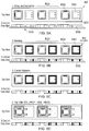
- FIGS. 1A-1C which may be collectively referred to as FIG. 1 , illustrate a semiconductor wafer and respective singulated die
- FIGS. 2A-2C which may be collectively referred to as FIG. 2 , illustrate a semiconductor wafer and respective singulated die
- FIG. 3 illustrates a MEMS microphone package
- FIG. 4 illustrates another type of transducer package
- FIGS. 5A-5C which may be collectively referred to as FIG. 5 , illustrate a semiconductor wafer and primary die according to a first example
- FIGS. 6A-6C which may be collectively referred to as FIG. 6 , illustrate a semiconductor wafer and primary die according to a second example
- FIGS. 7A-7D which may be collectively referred to as FIG. 7 , illustrate various views of a semiconductor wafer, and corresponding primary die according to a further example
- FIGS. 8A and 8B which may be collectively referred to as FIG. 8
- FIGS. 9A-9D which may be collectively referred to as FIG. 9
- FIG. 9 illustrate a process of fabricating a support structure similar to that shown in FIG. 7D ;
- FIGS. 10A and 10B which may be collectively referred to as FIG. 10 , illustrate a semiconductor wafer, and corresponding primary die, according to a further example
- FIGS. 11A and 11B which may be collectively referred to as FIG. 11 , illustrate a semiconductor wafer, and corresponding substrate die, according to a further example
- FIGS. 12A-12F which may be collectively referred to as FIG. 12 , and FIGS. 13, 14 and 15 , show various different structures according to further examples;
- FIG. 16 shows a cap wafer according to one example
- FIG. 17 shows a transducer package comprising a primary die which is similar to the primary die illustrated in FIG. 7D .
- the present examples relate generally to support structures for supporting electronic and/or electromechanical components and/or systems.
- Such support structures are typically fabricated from a wafer of semiconductor material.
- FIG. 1 illustrates a semiconductor wafer and respective singulated die.
- FIG. 1A schematically illustrates a semiconductor wafer 10 comprising a plurality of wafer portions 100 .
- Each wafer portion 100 defines a die and is processed to form a transducer 200 such as a MEMS capacitive transducer.
- FIG. 1B illustrates a single, or discrete, transducer die 100 formed following dicing of the wafer and comprising the transducer 200 .
- FIG. 1C provides an illustrative cross-sectional view through the line A-A of the discrete, or monolithic, die 100 illustrated in FIG. 1B .
- FIG. 2 illustrates a semiconductor wafer and respective singulated die.
- FIG. 2A schematically illustrates a semiconductor wafer 10 comprising a plurality of wafer portions 100 ′.
- each wafer portion 100 ′ defines a die which comprises a transducer component 200 and electronic circuit component.
- the electronic circuitry may be provided for the operation of, and/or with, the transducer 200 and will be electrically and operatively coupled to the transducer.
- FIG. 2B illustrates a single die 100 comprising the transducer 200 and the circuitry 300 that are both integrated on the same substrate.
- FIG. 2C which provides an illustrative cross-sectional view through the line A-A of the die illustrated in FIG. 2B , the circuit portion 300 is typically fabricated at the upper surface of the die 100 extending into the upper surface of the die.
- Semiconductor components including MEMS devices and/or electronic circuitry are typically housed within a package which allows easy handling and assembly and serves to protect the device from e.g. mechanical damage, RF noise and environmental contamination.
- the package also provides a means for electrically and mechanically connecting the package to a circuit board or other elements.
- a package for a MEMS transducer typically comprises a package substrate, which may be formed of a printed circuit board (PCB), and a cover portion which extends in a plane overlying the upper surface of the package substrate supported by side walls.
- the cover portion and side walls may be provided by a metallic lid which is attached to the upper surface of the package substrate.
- the cover portion and the side walls may be formed of two further PCBs.
- the three PCBs are bonded together wherein the middle PCB comprises an opening which defines the chamber of the package.
- One or more die are mounded to the upper surface of the package substrate within the chamber for example a MEMS transducer die and a circuitry die (IC).
- IC circuitry die
- FIG. 3 illustrates a previously proposed MEMS microphone package 400 a comprising a package substrate 450 and a cover 401 .
- a semiconductor substrate 100 comprising a MEMS transducer 200 is housed inside the package.
- the cover 401 is located over the transducer chip 100 and is attached to a first surface of the package substrate.
- the cover 401 may be a metallic lid.
- the transducer 200 may be a MEMS microphone and an aperture 402 in the cover 401 provides a sound port in order to allow acoustic signals to enter the package and stimulate the transducer.
- the transducer 200 is electrically coupled to the package substrate 450 via bond pads on the transducer and the upper surface of the package substrate and bond wires.
- the package may house a chip 100 ′ comprising a transducer and integrated circuitry similar to the example illustrated in FIGS. 2B and 2C .
- FIG. 4 illustrates another type of previously proposed transducer package 400 b .
- the package houses a transducer chip 100 comprising a transducer 200 and a discrete integrated circuit (IC) 350 .
- the transducer 100 and IC 350 are co-packaged.
- the IC 350 is electrically connected to the transducer 200 and is also electrically bonded to the package substrate 450 .
- the IC 350 is bonded to the transducer and package substrate via wire-bonds.
- a cover 410 is located on the package substrate 450 so as to enclose the transducer 200 and the IC 350 .
- the cover 410 comprises an upper part or lid portion 410 a and a side wall 410 b which are all typically formed of PCB, i.e. FR4.
- the transducer is a microphone transducer and the cover 410 has a sound port 402 in the upper part 410 a which allows acoustic signals to enter the package.
- the transducer die and/or the circuitry die are discrete components that are mounted on the first, upper surface of the package substrate.
- the placement of the chip typically by an automated “pick-and-place” cycle, requires a high degree of accuracy and repeatability which can be difficult to achieve.
- FIGS. 5A-5C illustrate a first example.
- FIG. 5A illustrates a plan view of a semiconductor wafer 50 according to a first example.
- the semiconductor wafer 50 comprises a plurality of wafer portions and at least some of the wafer portions can be considered to define a primary die.
- Each primary die 500 comprises a hole or aperture 501 in the wafer material which extends all the way through the wafer portion from an upper surface of the wafer substrate to a lower surface of the wafer substrate.
- the hole can be considered to be region where the semiconductor material of the wafer has been removed or is absent.
- the hole or aperture can be considered to connect a region directly above the upper surface of the respective wafer portion to a region directly below the lower surface of the wafer portion.
- the aperture can be considered to expose an opening in both the upper and lower surfaces of the semiconductor wafer portion. It should be noted that the hole or aperture has an unimpeded path to light, fluids etc., after the wafers semiconducting process steps have been completed.
- the plurality of holes may be formed as part of a wafer level processing step such as etching.
- the structure shown in FIG. 5A can be considered to be a semiconductor wafer lattice.
- a plurality of the wafer portions will each define a discrete, or monolithic, primary die 500 .
- the step of dicing the wafer may take place when the wafer is in the state illustrated in FIG. 5A .
- dicing of the wafer may take place following the completion of one or more, further “wafer level” processing stages—i.e. processing stages that are performed on the wafer as a whole and before the wafer is diced.
- Additional wafer-level processing stages may, for example, include providing and securing one or more secondary dies within the apertures 501 , the deposition of one or more layers such as redistribution layers to the upper and/or lower surface of the wafer or a wafer level packaging process for covering the plurality of the wafer portions.
- processes according to one or more examples of the present aspects may generate a plurality of intermediate products.
- FIG. 5C provides an illustrative cross-sectional view of the discrete primary die 500 taken along the line A-A′ of FIG. 5B .
- the primary die 500 can be considered to be a primary substrate or blank die substrate (BDS) and may form a substrate e.g. in a package structure.
- BDS blank die substrate
- a primary die 500 may be provided with one or more through silicon vias (TSV) and associated bond pads that are created as part of the wafer-level processing.
- TSV through silicon vias
- a TSV is a vertical electrical connection that passes completely through the silicon die and may be used, in conjunction with an associated bond pad, as an electrical interconnect to the next level of interconnect.
- the primary die acts as a substrate e.g.
- each hole or aperture 501 defines a region absent of wafer material formed within the die between a first, upper plane X and a second, lower plane Y.
- the upper plane X is defined by (i.e. is coincident with) the first, upper surface of the primary die (or wafer substrate) whilst the lower plane Y is defined by (i.e. coincident with) the second, lower surface of the primary die (or wafer substrate).
- the holes or apertures 501 that are provided in the wafer material are suitable for receiving a discrete die or IC.
- the hole is sufficiently sized to at least partially accommodate a discrete substrate portion.
- the wafer portion which defines a die 500 can be considered to be a primary or parent die, whilst the discrete die that is intended to be received within the hole 501 can be considered to be a secondary or child die.
- a secondary die may also be considered to be a secondary substrate.
- the hole is rectangular in shape and is defined by a length x, a width y and a depth z.
- the hole may be any other shape, including but not limited to: circular; hexagonal; square; rectangular; “L” shaped; or “C” shaped, provided that it is suitable for receiving a secondary semiconductor die.
- the hole may be sufficiently sized to accommodate the planar dimensions—i.e. the x (width) and y (length) dimensions—of the intended secondary die.
- the planar dimensions of the hole are slightly larger than the planar dimensions of the intended secondary die.
- the secondary die fits within the aperture when oriented such that the plane of the secondary die is substantially aligned with or parallel to the plane of the wafer.
- each wafer portion or semiconducting primary die may comprise a plurality of apertures, each aperture extending through the wafer portion or substrate die from an upper surface thereof to a lower surface thereof. Each aperture is suitable for receiving at least one secondary die.
- FIGS. 12A to 12F show various different substrate structures comprising one or more non-limiting example apertures. Specifically, FIGS. 12A and 12B show a primary die portion forming a substrate and comprising a single hole H 1 . FIGS. 12C and 12D show a primary die portion forming a substrate and comprising a first hole H 1 and a second hole H 2 .
- FIG. 12E shows a square-shaped primary die portion comprising four holes H 1 -H 4 .
- a primary or BDS offers a versatile structure for supporting a plurality and/or range of mechanical, electrical and/or electromechanical components, devices and/or systems including for example, ICs and/or MEMS transducers.
- a single primary die or BDS may be provided with at least two different types of mechanical, electrical and/or electromechanical components, thus facilitating the integration of a various different components of a system within the substrate of a single, i.e. monolithic, die. This offers the potential for considerable space savings and package manufacturing processing steps, cost of packaging, etc.
- FIG. 6 shows an expanded view of part of a wafer comprising a row of wafer portions, each of the wafer portions defining a primary die 500 .
- FIG. 6A shows the row of wafer portions in plan view whilst FIG. 6B provides a cross-sectional view.
- a secondary or “child” die 550 is provided in each of the apertures 501 formed in the wafer portions 500 .
- each of the secondary die are supported within the respective aperture by means of a filler, or support, material 520 .
- the adhesive or bonding material 520 is introduced into the space between the primary and secondary die by overmoulding, as will be understood by those skilled in the art.
- the secondary die may be e.g. a transducer die or a circuitry die. It will be appreciated that the secondary die provided within the apertures of at least one row of wafer portions or within the apertures of the whole wafer may all share the same function and may themselves have been fabricated as part of a batch e.g. wafer-level, fabrication process. Thus, the wafer may be considered to be homogeneous in terms of the type, functionality or class of secondary chips that are provided within the apertures of the wafer or wafer row. Alternatively, the one or more of the secondary dies may be different to one or more other secondary die, either in the same row or in a different row, in terms of the function of the secondary dies.
- the wafer may be considered to be heterogeneous in terms of the type of class of secondary chips that are provided within the apertures of the wafer or wafer row.
- one or more of the apertures are provided with a discrete MEMS transducer die, such as a MEMS microphone transducer die.
- one or more of the apertures are provided with a discrete circuitry die, such as an IC.
- the wafer may be supported on a carrier 530 as is known in the art.
- the plurality of secondary die may be placed within the apertures so as to leave a lateral gap or clearance between the outer perimeter surface of the secondary die and the surface of the wafer material which defines the boundary shape of the respective aperture 501 .
- a fluid filler or support material 520 such as epoxy resin for example, may be supplied so as to fill the lateral gap.
- the carrier usually in the form of a sheet, may be removed at a later stage once the filler material has hardened or set, and the secondary die is thus secured or fixedly supported within the aperture.
- FIG. 6C illustrates the singulated wafer portion 500 which can be considered to be a primary or parent die.
- the primary die 500 comprises a secondary or child die supported (e.g. embedded or encapsulated) within an aperture 501 .
- the aperture 501 can be considered to be a region of absence of the semiconductor wafer material. Thus, even though as illustrated in FIG. 6C the aperture or hole has been filled with the secondary die and filler material, there is nonetheless a region 501 where the wafer material is absent.
- a discrete secondary die can be considered to be integrated within the silicon substrate, or primary die, defined by the wafer portion 500 . In particular, the secondary die is integrated within the plane of the primary die.
- the primary die may be provided with TSV's and associated bond pads (not shown).
- non-semiconductor wafer level processing may take place before dicing of the wafer takes place, e.g. in order to provide one or more redistribution layers for one or more electrical connections between the primary and secondary.
- redistributions layers being applied to the whole wafer in a batch process as will be understood by those of ordinary skill in the art.
- each wafer portion comprises two more holes or apertures, each aperture being suitable for receiving a discrete secondary die.
- each of the holes is sufficiently sized to receiving another discrete die portion.
- the discrete die may be supported within a given aperture of the wafer portion by means of a filler material.
- the apertures may be sufficiently sized such that the planar dimensions of a given aperture or hole are larger than the planar dimensions of the intended chip.
- a first hole of a given primary die may comprise a transducer die, such as a MEMS microphone transducer die, whilst the second hole of the said primary die may comprise a circuitry die, such as an IC for receiving output signals from the transducer chip.
- the primary die comprises two embedded secondary die which can be considered to be integrated within the same primary die substrate. Electrical connections may be advantageously formed between the embedded secondary die using one or more metal layers or redistribution layers and/or at least one TSV.
- FIG. 7 illustrates various views of a semiconductor wafer, and corresponding primary die, comprising a MEMS transducer and an aperture.
- FIG. 7A illustrates a plan view of a semiconductor wafer 70 comprising a plurality of wafer portions according to a second example at least some of the wafer portions defining a primary die 700 .
- Each primary die 700 has been processed in a first transducer region T of the primary die to provide a MEMS transducer 702 .
- the MEMS transducer comprises a MEMS microphone transducer.
- other types of transducer such as an accelerometer, gyroscope etc., may be fabricated and/or provided in a transducer region T of each of the primary die regions. Examples are also envisaged wherein each primary die may be provided with more than one transducer.
- each primary die 700 has been processed in a second aperture region A of the wafer portion to form a hole or aperture 701 in the wafer material.
- the resultant structure is therefore a primary die or primary substrate comprising a MEMS transducer formed in a transducer region T of the die and an aperture formed in an aperture region A of the die.
- step of dicing the wafer may take place when the wafer is in the state illustrated in FIG. 7A but may also take place following additional wafer level processing stages.
- multiple intermediate products are formed during intermediate steps of a fabrication process.
- FIG. 7C provides a cross-sectional view of the discrete primary die 700 taken along the line A-A′ of FIG. 7B .
- the hole 701 defines a region absent of the wafer material formed within the substrate 700 between a first, upper plane X and a second, lower plane Y.
- the upper plane X is defined by (i.e. is coincident with) the first, upper surface of the primary die whilst the lower plane Y is defined by (i.e. coincident with) the second, lower surface of the primary die.
- the MEMS microphone transducer comprises a flexible membrane 710 which overlies a cavity 708 formed in the lower surface of the wafer portion 700 .
- the hole or aperture 701 provided in the aperture region of the primary die extends completely through the wafer portion 700 from a first opening in the upper surface of the wafer substrate to a second opening in the lower surface of the wafer substrate.
- the opening in the upper surface of the primary die that is defined by the aperture allows a secondary die to be located within the aperture via the first opening, from a region directly above the wafer.
- the hole 701 in the wafer material is suitable for receiving a discrete die or chip.
- the hole is sufficiently sized to at least partially accommodate another discrete die.
- the substrate 700 can be considered to be a primary or parent die, whilst the die that is intended to be received within the hole 701 can be considered to be a secondary or child die.
- the hole is rectangular in shape and is defined by a length x, a width y and a depth z.
- the hole may be any other shape provided it is suitable for receiving a secondary die.
- the hole may be sufficiently sized to accommodate the planar dimensions—i.e. the x and y dimensions—of the secondary die.
- the planar dimensions of the hole are slightly larger than the planar dimensions of the intended secondary die.
- a secondary die which may be a device or circuitry die—located within the aperture of the primary die.
- a primary die 700 comprises a semiconductor substrate and a MEMS transducer 702 formed in a transducer region of the substrate.
- a secondary die 720 is located within the MEMS transducer substrate in the aperture region.
- the secondary die comprises a discrete die which is supported between the upper and lower planar surfaces of the substrate. In this sense the secondary die can be considered to be provided within the plane of the primary die. Due to the way in which the secondary die will typically be located within the aperture with the aid of a carrier sheet, the lower planar surface of the secondary die will be substantially flush with (i.e.
- the MEMS transducer may be electrically connected to the secondary die 720 by means of wire bonding or, advantageously, through one or more redistribution layers (not shown) applied to the upper and/or lower surface of the primary die.
- each wafer portion defining a primary die may comprise a plurality of apertures, each aperture extending through the wafer portion or substrate die from an upper surface thereof to a lower surface thereof. Each aperture is suitable for receiving at least one secondary die.
- FIG. 13 shows a number of variations or modifications of the primary die illustrated in FIG. 7B .
- the die 700 which can be considered to be a primary die, is provided with a single MEMS transducer.
- the primary die is also provided with one or more holes or apertures 701 a . . . h , each aperture being suitable for receiving at least one discrete secondary die or semiconductor die.
- FIG. 7D A process of fabricating a support structure similar to that shown in FIG. 7D will now be described with reference to FIGS. 8 and 9 .
- FIG. 8A shows a semiconductor wafer 80 .
- One or more of the wafer portions of the wafer portion defines a primary die 800 and is processed to provide a MEMS microphone transducer 802 and an aperture 801 which extends through the semiconductor material of the wafer portion from an upper surface to a lower surface thereof.
- the wafer is processed to provide a MEMS microphone transducer structure on each wafer portion.
- a transducer cavity (not shown) is formed in the lower surface (back side) of the primary die 800 in a region underlying the MEMS microphone transducer structure 802 .
- the cavity may either allow acoustic pressure waves to be incident on a flexible membrane of the MEMS microphone transducer 802 or provide a back-volume for the transducer 802 .
- the process of forming at least a portion of the aperture 801 may take place at the same time as forming the transducer cavity e.g. by an etching process. It will be appreciated, however, that since the transducer cavity does not extend all the way through the die, the start time of the etching process to form the aperture may be in advance of the start time of the etching process to form the cavity.
- FIG. 8B illustrates another wafer 85 .
- the wafer 85 comprises a plurality of wafer portions one or more of which define a circuitry die region.
- the wafer 85 is diced to form a plurality of circuitry die 850 .
- Each circuitry die may be, e.g. an IC for processing the output of the transducer device 802 .
- FIGS. 9A to 9D illustrate a series of stages in a wafer level processing flow for processing of the wafer 80 shown in FIG. 8A .
- FIGS. 9A to 9E illustrates a top plan view and a cross-sectional view of a part of the wafer 80 ′.
- a moulding step involves supplying e.g. injecting, a moulding material 840 such as an epoxy mould material.
- the resultant structure shown in FIG. 9C can be considered to be a composite or hybrid structure comprising a planar frame or lattice of semiconductor wafer material and a plurality of discrete secondary die at least partially buried or encapsulated within the plane of the wafer. According to the illustrated example the lower planar surfaces of the discrete secondary die are flush with the lower planar surface of the wafer.
- FIG. 9D illustrates a process of applying a redistribution layer by a RDL process.
- a RDL or redistribution process typically involves providing a metal, e.g. copper, plating on the top surface of the processed wafer in order to redistribute or relocate electrical connections as will be understood by those of ordinary skill in the art.
- the RDL process will typically involve:
- FIG. 10 illustrates a semiconductor wafer, and corresponding substrate die, comprising circuitry and an aperture.
- FIG. 10A illustrates a plan view of a semiconductor wafer 90 according to a further example.
- the wafer 90 comprises a plurality of wafer portions 900 according to a further example.
- Each wafer portion 900 has been processed in a circuitry region C of the wafer portion to provide electronic circuitry.
- each wafer portion 900 has been processed in an aperture region A of the wafer portion to form a hole or aperture 901 through the wafer material.
- the hole or aperture 901 extends through the wafer portion 900 from an opening in the upper surface of the wafer substrate to an opening in the lower surface of the wafer substrate.
- each wafer portion will define a discrete substrate 900 following dicing of the semiconductor wafer.
- the resultant structure is therefore a substrate portion or substrate die comprising circuitry provided in the circuitry region C of the die and an aperture formed in an aperture region A of the die.
- FIG. 14 shows a number of different substrate dies according to variations of the substrate die illustrated in FIG. 10B .
- the die 900 which can be considered to be a primary die, is provided with a circuitry region comprising electronic circuitry 920 .
- the primary die is also provided with one or more holes or apertures 901 a . . . h , each aperture being suitable for receiving at least one discrete secondary die.
- FIG. 11 illustrates a semiconductor wafer, and corresponding primary die, comprising a MEMS transducer, circuitry and an aperture.
- FIG. 11A illustrates a plan view of a semiconductor wafer 60 comprising a plurality of wafer portions 600 according to a further example.
- Each wafer portion 600 has been processed in a circuitry region C of the wafer portion, i.e. die, to provide integrated electronic circuitry.
- Each wafer portion 600 has also been processed in a transducer region T of the wafer portion to provide a MEMS transducer 602 .
- transducer region T of each of the wafer portions may be fabricated and/or provided in a transducer region T of each of the wafer portions.
- each wafer portion 600 has been processed in an aperture region A of the wafer portion to form a hole or aperture 601 in the wafer material.
- the hole or aperture 601 extends through the wafer portion 900 from an opening in the upper surface of the wafer substrate to an opening in the lower surface of the wafer substrate.
- each wafer portion will define a discrete substrate 600 following dicing of the semiconductor wafer.
- FIG. 15 shows a number of different substrate dies according to variations of the substrate die illustrated in FIG. 11B .
- the die 1000 which can be considered to be a primary die, is provided with a single circuitry region and a single transducer region 702 .
- the primary die is also provided with one or more holes or apertures H 1 . . . H 6 each aperture being suitable for receiving at least one discrete secondary substrate die.
- the die or wafer portion of a wafer is provided with a MEMS microphone transducer which can be considered to be an input transducer.
- MEMS microphone transducer which can be considered to be an input transducer.
- Microphone devices formed using MEMS fabrication processes typically comprise one or more membranes with electrodes for read-out/drive deposited on the membranes and/or a substrate.
- the read out is usually accomplished by measuring the capacitance between the electrodes.
- an output transducer such as MEMS speakers for example, the membrane is moved by electrostatic forces generated by varying a potential difference applied across the electrodes.
- a singulated primary die according to an example of the present aspects will preferably be housed within a package which allows easy handling and assembly and serves to protect the primary die and the components supported thereby—e.g. secondary die—from e.g. mechanical damage, RF noise and environmental contamination.
- the package also provides a means—e.g. an external conductive contact—for connecting the package to a circuit board or other elements.
- the creation of a package for an electronic system involves numerous processing steps and stages. In conventional packaging techniques, the finished wafer is diced into individual chips which are then bonded to a packaging substrate and encapsulated. Wafer-level packaging involves packaging the chips whilst they are still part of the wafer and prior to dicing into individual packages.
- FIG. 16 shows a cap wafer 1100 comprising a plurality of cap wafer portions 1010 . At least some of the cap wafer portions 1010 is processed to comprise a recessed area 1020 .
- the recessed area may optionally be plated with a metal material in order to act as a barrier to RF noise and interference.
- the wafer can be considered to be a cap wafer since each of the cap wafer portions defines a cap portion (or lid) for a respective wafer portion of a primary die wafer.
- a cap wafer as illustrated in FIG. 16 may be arranged relative to a semiconductor wafer according to an example of the present aspects in order to define a package.
- the recessed area of a given cap wafer portion defines side walls which are mounted to the upper surface of a primary substrate wafer portion in a process known as wafer to wafer bonding.
- the cap portion in conjunction with the primary die defines a package chamber.
- the primary die forms the package substrate, with the lid structure being mounted on the primary die and thus obviating the need for a separate package substrate.
- a package incorporating a primary die according to one or more the present examples which acts as the package substrate beneficially achieves a reduction in overall package height.
- a package which houses a microphone transducer will typically have a sound port to allow transmission of sound waves to/from the transducer within the package and the transducer may be configured so that the flexible membrane is located between first and second volumes, i.e. spaces/cavities that may be filled with air (or some other gas suitable for transmission of acoustic waves), and which are sized sufficiently so that the transducer provides the desired acoustic response.
- the sound port acoustically couples to a first volume on one side of the transducer membrane, which may sometimes be referred to as a front volume.
- the second volume sometimes referred to as a back volume, on the other side of the one or more membranes is generally required to allow the membrane to move freely in response to incident sound or pressure waves, and this back volume may be substantially sealed (although it will be appreciated by one skilled in the art that for MEMS microphones and the like the first and second volumes may be connected by one or more flow paths, such as small holes in the membrane, that are configured so as present a relatively high acoustic impedance at the desired acoustic frequencies but which allow for low-frequency pressure equalisation between the two volumes to account for pressure differentials due to temperature changes or the like).
- the primary die comprises a MEMS microphone transducer and wherein the cavity of the MEMS microphone transducer is formed in the underside of the primary die, the cavity may also be considered to form the sound port of the package.
- FIG. 17 shows a transducer package comprising a primary die 700 which is similar to the primary die illustrated in FIG. 7D .
- the primary die comprises a MEMS transducer 702 formed in a transducer region of the substrate.
- a secondary die 720 is embedded within an aperture of the primary die (which forms the MEMS transducer substrate), the aperture being defined between the upper and lower planar surfaces of the primary die.
- the primary die further comprises a plurality of TSVs 703 which extend through the plane of the substrate from an internal bond pad 704 to an external bond pad 705 .
- An RDL layer 706 is provided on the upper surface of the primary die.
- a cap portion 1010 is mounted on an upper surface of the primary die to define the back volume of the MEMS microphone transducer 702 .
- the secondary die may exhibit a depth that is less than, equal to, or greater than the depth (z-dimension) of the aperture.
- the chamber will form the back volume of the microphone transducer.
- an ASIC within an aperture of the primary die—in other words within the same substrate that forms the cavity of the transducer—and to achieve a gain in headroom inside the chamber and/or a reduction in package height in comparison to previously proposed microphone transducers.
- the aperture of the primary die may be provided with a secondary die that is fabricated according to a process node or technology scale that is different to the process node of the primary die.
- the semiconductor wafer may be fabricated according to a 55 nm technology node process for example, whilst the secondary chip may have been fabricated by a 80 nm, 22 nm or even 7 nm technology processing node.
- semiconductor material include, but is not limited to, any and all: Group IV elemental/compound semiconductors; Group VI elemental semiconductors; Group III-V, II-VI, I-VII, IV-VI, V-VI, II-V, I-III-VI 2 semiconductors; oxides; layered, magnetic and/or organic semiconductors.
- MEMS sensor transducers especially capacitive transducers such as MEMS microphones.
- MEMS capacitive sensors could be implemented, for example accelerometers, pressure sensors, proximity sensors or flow meters.
- Examples of the present aspects may be implemented in a host device, especially a portable and/or battery powered host device such as a mobile telephone, an audio player, a video player, a PDA, a mobile computing platform such as a laptop computer or tablet and/or a games device for example or in an accessory device, such a headset, earbud (possibly noise-cancelling), or microphone assembly, designed for wired, or wireless connection with such host devices, possibly via multi-wire cables, multi-pole jacks, or optical fibres and connectors.
- a host device especially a portable and/or battery powered host device such as a mobile telephone, an audio player, a video player, a PDA, a mobile computing platform such as a laptop computer or tablet and/or a games device for example or in an accessory device, such a headset, earbud (possibly noise-cancelling), or microphone assembly, designed for wired, or wireless connection with such host devices, possibly via multi-wire cables, multi-pole jacks, or optical fibres and connectors.
- references in the appended claims to an apparatus or system or a component of an apparatus or system being adapted to, arranged to, capable of, configured to, enabled to, operable to, or operative to perform a particular function encompasses that apparatus, system, or component, whether or not it or that particular function is activated, turned on, or unlocked, as long as that apparatus, system, or component is so adapted, arranged, capable, configured, enabled, operable, or operative. Accordingly, modifications, additions, or omissions may be made to the systems, apparatuses, and methods described herein without departing from the scope of the disclosure. For example, the components of the systems and apparatuses may be integrated or separated.
- each refers to each member of a set or each member of a subset of a set.
Landscapes
- Engineering & Computer Science (AREA)
- Microelectronics & Electronic Packaging (AREA)
- Physics & Mathematics (AREA)
- Manufacturing & Machinery (AREA)
- Acoustics & Sound (AREA)
- Signal Processing (AREA)
- Computer Hardware Design (AREA)
- Health & Medical Sciences (AREA)
- General Health & Medical Sciences (AREA)
- Toxicology (AREA)
- Electromagnetism (AREA)
- Micromachines (AREA)
Abstract
Description
-
- a MEMS transducer provided in a transducer region of the die, wherein the semiconductor wafer material of the primary die forms a substrate of the MEMS transducer.
-
- a circuitry region, the circuitry region comprising at least one circuitry component in the circuitry region.
-
- a MEMS transducer formed in a transducer region of the wafer portion;
- a region of absence, the region of absence being a region where the material of the semiconductor wafer has been removed, the region of absence extending between a first plane defined by the upper surface of the wafer and a second plane defined by the lower surface of the wafer portion.
ii) a secondary substrate, the secondary substrate having a length and a width;
-
- wherein the aperture of a given wafer portion of the semiconductor wafer exhibits a length and a width that is greater than or equal to the length and width of the secondary substrate.
-
- applying a first layer of insulator, e.g. a dielectric material, that will leave exposed only the bond pad interface on the respective die;
- applying a copper patterning which will ensure appropriate electrical connection between the respective bond pad interfaces that will be used for soldering (such as I/O pads and lid track in case of use of metal lid); and
- applying a second dielectric which will protect the copper surface of the electrical connection from oxidation.
- Statement 1A. A semiconductor wafer comprising a plurality of wafer portions, each wafer portion defining a primary substrate and comprising at least one aperture extending through the semiconductor wafer from an upper surface of the semiconductor wafer to a lower surface of the semiconductor wafer, wherein the aperture is suitable for receiving a secondary substrate. [
- Statement 1B. A semiconductor wafer comprising a plurality die, at least one die comprising an aperture extending through the die between upper and lower surfaces of the die, wherein the aperture is suitable for receiving a semiconductor die.
- Statement 1Ba. A semiconductor wafer comprising a plurality of first die, at least one first die comprising an aperture extending through the die between upper and lower surfaces of the die, wherein the aperture is suitable for receiving a semiconductor second die.
- Statement 1C. A semiconductor wafer comprising a plurality die, wherein a subset plurality of die each comprise an aperture extending through the die between upper and lower surfaces of the die, wherein the aperture is suitable for receiving a semiconductor die.
- Statement 1D. A semiconductor wafer comprising a plurality die, each die comprising an aperture extending through the die between upper and lower surfaces of the die, wherein the aperture is suitable for receiving a semiconductor die.
- Statement 2A. A first semiconductor die comprising an aperture extending between its upper and lower surfaces, wherein the aperture is suitable for receiving a second semiconductor die.
- Statement 3A. A semiconductor wafer comprising a plurality die, at least one die comprising a MEMS transducer in a transducer region and an aperture extending through the die between upper and lower surfaces of the die in an aperture region, wherein the aperture is suitable for receiving a semiconductor die.
- Statement 3B. A semiconductor wafer comprising a plurality of first die, at least one first die comprising a MEMS transducer in a transducer region and an aperture extending through the at least one first die between upper and lower surfaces of the at least one first die in an aperture region, wherein the aperture is suitable for receiving a semiconductor second die.
- Statement 4A. A first semiconductor die comprising a MEMS transducer in a transducer region and an aperture extending between its upper and lower surfaces in an aperture region, wherein the aperture is suitable for receiving a second semiconductor die.
- Statement 5A. A semiconductor wafer comprising a plurality die, at least one die comprising electronic circuitry in a circuit region and an aperture extending through the die between upper and lower surfaces of the die in an aperture region, wherein the aperture is suitable for receiving a semiconductor die.
- Statement 5B. A semiconductor wafer comprising a plurality of first die, at least one first die comprising electronic circuitry in a circuit region and an aperture extending through the at least one first die between upper and lower surfaces of the at least one first die in an aperture region, wherein the aperture is suitable for receiving a semiconductor second die.
- Statement 6A. A first semiconductor die comprising electronic circuitry in a circuit region and an aperture extending between its upper and lower surfaces in an aperture region, wherein the aperture is suitable for receiving a second semiconductor die.
- Statement 7A. A semiconductor wafer comprising a plurality die, at least one die comprising a MEMS transducer in a transducer region, electronic circuitry in a circuit region and an aperture extending through the die between upper and lower surfaces of the die in an aperture region, wherein the aperture is suitable for receiving a semiconductor die.
- Statement 8. A first semiconductor die comprising a MEMS transducer in a transducer region, electronic circuitry in a circuit region and an aperture extending between its upper and lower surfaces in an aperture region, wherein the aperture is suitable for receiving a second semiconductor die.
Claims (10)
Priority Applications (2)
| Application Number | Priority Date | Filing Date | Title |
|---|---|---|---|
| US16/822,771 US11223907B2 (en) | 2019-03-22 | 2020-03-18 | Semiconductor structures |
| US17/520,386 US11736866B2 (en) | 2019-03-22 | 2021-11-05 | Semiconductor structures |
Applications Claiming Priority (11)
| Application Number | Priority Date | Filing Date | Title |
|---|---|---|---|
| US201962822268P | 2019-03-22 | 2019-03-22 | |
| GB1905921 | 2019-04-29 | ||
| GB1905923.7 | 2019-04-29 | ||
| GB1905923 | 2019-04-29 | ||
| GB1905921.1A GB2582382B (en) | 2019-03-22 | 2019-04-29 | Semiconductor structures |
| GB1905922.9A GB2582383A (en) | 2019-03-22 | 2019-04-29 | Semiconductor structures |
| GB1905921.1 | 2019-04-29 | ||
| GB1905922.9 | 2019-04-29 | ||
| GB1905922 | 2019-04-29 | ||
| GB1905923.7A GB2582384B (en) | 2019-03-22 | 2019-04-29 | Semiconductor structures |
| US16/822,771 US11223907B2 (en) | 2019-03-22 | 2020-03-18 | Semiconductor structures |
Related Child Applications (1)
| Application Number | Title | Priority Date | Filing Date |
|---|---|---|---|
| US17/520,386 Continuation US11736866B2 (en) | 2019-03-22 | 2021-11-05 | Semiconductor structures |
Publications (2)
| Publication Number | Publication Date |
|---|---|
| US20200304920A1 US20200304920A1 (en) | 2020-09-24 |
| US11223907B2 true US11223907B2 (en) | 2022-01-11 |
Family
ID=66809082
Family Applications (2)
| Application Number | Title | Priority Date | Filing Date |
|---|---|---|---|
| US16/822,771 Active US11223907B2 (en) | 2019-03-22 | 2020-03-18 | Semiconductor structures |
| US17/520,386 Active US11736866B2 (en) | 2019-03-22 | 2021-11-05 | Semiconductor structures |
Family Applications After (1)
| Application Number | Title | Priority Date | Filing Date |
|---|---|---|---|
| US17/520,386 Active US11736866B2 (en) | 2019-03-22 | 2021-11-05 | Semiconductor structures |
Country Status (5)
| Country | Link |
|---|---|
| US (2) | US11223907B2 (en) |
| EP (1) | EP3941875A1 (en) |
| CN (1) | CN113631500A (en) |
| GB (3) | GB2582384B (en) |
| WO (1) | WO2020193955A1 (en) |
Families Citing this family (6)
| Publication number | Priority date | Publication date | Assignee | Title |
|---|---|---|---|---|
| WO2016102924A1 (en) * | 2014-12-23 | 2016-06-30 | Cirrus Logic International Semiconductor Limited | Mems transducer package |
| US11432056B1 (en) * | 2019-07-26 | 2022-08-30 | Acacia Communications, Inc. | Switch |
| CN111918191A (en) * | 2020-07-24 | 2020-11-10 | 钰太芯微电子科技(上海)有限公司 | Combined packaged microphone |
| DE102020211741A1 (en) * | 2020-09-21 | 2022-03-24 | Robert Bosch Gesellschaft mit beschränkter Haftung | Micromechanical sensor |
| US11760627B2 (en) | 2021-06-10 | 2023-09-19 | Invensense, Inc. | MEMS stress reduction structure embedded into package |
| US20230402333A1 (en) * | 2022-06-10 | 2023-12-14 | Qorvo Us, Inc. | System in a package (sip) with air cavity and epoxy seal |
Citations (9)
| Publication number | Priority date | Publication date | Assignee | Title |
|---|---|---|---|---|
| GB2202673A (en) | 1987-03-26 | 1988-09-28 | Haroon Ahmed | Multiplechip assembly |
| EP0478426A1 (en) | 1990-09-28 | 1992-04-01 | Thomson-Csf | Method of fabrication for a hybrid module |
| US20100047567A1 (en) | 2008-07-21 | 2010-02-25 | Commissariat A L'energie Atomique | Multi-component device integrated into a matrix |
| US20100195299A1 (en) * | 2007-06-07 | 2010-08-05 | Commissariat A L'energie Atomique | Integrated multicomponent device in a semiconducting die |
| US20140264647A1 (en) | 2013-03-15 | 2014-09-18 | Rakesh Katragadda | Method of forming monolithic cmos-mems hybrid integrated, packaged structures |
| US20170313579A1 (en) | 2016-04-28 | 2017-11-02 | Stmicroelectronics S.R.L. | Multi-chamber transducer module, apparatus including the multi-chamber transducer module and method of manufacturing the multi-chamber transducer module |
| US20180146302A1 (en) | 2014-07-31 | 2018-05-24 | Merry Electronics (Shenzhen) Co., Ltd. | Mems microphone package structure and method for manufacturing the mems microphone package structures |
| US20180233469A1 (en) | 2013-10-31 | 2018-08-16 | Infineon Technologies Ag | Device including semiconductor chips and method for producing such device |
| US20180295458A1 (en) * | 2017-04-07 | 2018-10-11 | Infineon Technologies Ag | Mems sound transducer element and method for producing a mems sound transducer element |
Family Cites Families (2)
| Publication number | Priority date | Publication date | Assignee | Title |
|---|---|---|---|---|
| US7405108B2 (en) * | 2004-11-20 | 2008-07-29 | International Business Machines Corporation | Methods for forming co-planar wafer-scale chip packages |
| US10455309B2 (en) * | 2014-12-23 | 2019-10-22 | Cirrus Logic, Inc. | MEMS transducer package |
-
2019
- 2019-04-29 GB GB1905923.7A patent/GB2582384B/en active Active
- 2019-04-29 GB GB1905921.1A patent/GB2582382B/en active Active
- 2019-04-29 GB GB1905922.9A patent/GB2582383A/en not_active Withdrawn
-
2020
- 2020-03-18 US US16/822,771 patent/US11223907B2/en active Active
- 2020-03-19 WO PCT/GB2020/050736 patent/WO2020193955A1/en not_active Ceased
- 2020-03-19 EP EP20716864.2A patent/EP3941875A1/en not_active Withdrawn
- 2020-03-19 CN CN202080022911.8A patent/CN113631500A/en active Pending
-
2021
- 2021-11-05 US US17/520,386 patent/US11736866B2/en active Active
Patent Citations (9)
| Publication number | Priority date | Publication date | Assignee | Title |
|---|---|---|---|---|
| GB2202673A (en) | 1987-03-26 | 1988-09-28 | Haroon Ahmed | Multiplechip assembly |
| EP0478426A1 (en) | 1990-09-28 | 1992-04-01 | Thomson-Csf | Method of fabrication for a hybrid module |
| US20100195299A1 (en) * | 2007-06-07 | 2010-08-05 | Commissariat A L'energie Atomique | Integrated multicomponent device in a semiconducting die |
| US20100047567A1 (en) | 2008-07-21 | 2010-02-25 | Commissariat A L'energie Atomique | Multi-component device integrated into a matrix |
| US20140264647A1 (en) | 2013-03-15 | 2014-09-18 | Rakesh Katragadda | Method of forming monolithic cmos-mems hybrid integrated, packaged structures |
| US20180233469A1 (en) | 2013-10-31 | 2018-08-16 | Infineon Technologies Ag | Device including semiconductor chips and method for producing such device |
| US20180146302A1 (en) | 2014-07-31 | 2018-05-24 | Merry Electronics (Shenzhen) Co., Ltd. | Mems microphone package structure and method for manufacturing the mems microphone package structures |
| US20170313579A1 (en) | 2016-04-28 | 2017-11-02 | Stmicroelectronics S.R.L. | Multi-chamber transducer module, apparatus including the multi-chamber transducer module and method of manufacturing the multi-chamber transducer module |
| US20180295458A1 (en) * | 2017-04-07 | 2018-10-11 | Infineon Technologies Ag | Mems sound transducer element and method for producing a mems sound transducer element |
Non-Patent Citations (10)
| Title |
|---|
| Combined Search and Examination Report under Sections 17 and 18(3), UKIPO, Application No. GB1905921.1, dated Oct. 12, 2020. |
| Combined Search and Examination Report under Sections 17 and 18(3), UKIPO, Application No. GB1905921.1, dated Sep. 13, 2019. |
| Combined Search and Examination Report under Sections 17 and 18(3), UKIPO, Application No. GB1905922.9, dated Oct. 5, 2020. |
| Combined Search and Examination Report under Sections 17 and 18(3), UKIPO, Application No. GB1905922.9, dated Sep. 13, 2019. |
| Combined Search and Examination Report under Sections 17 and 18(3), UKIPO, Application No. GB1905923.7, dated Oct. 12, 2020. |
| Combined Search and Examination Report under Sections 17 and 18(3), UKIPO, Application No. GB1905923.7, dated Sep. 13, 2019. |
| Examination Report under Section 18(3), UKIPO, Application No. GB1905921.1, dated May 25, 2021. |
| Examination Report under Section 18(3), UKIPO, Application No. GB1905922.9, dated May 25, 2021. |
| Examination Report under Section 18(3), UKIPO, Application No. GB1905923.7, dated May 25, 2021. |
| International Search Report and Written Opinion of the International Searching Authority, International Application No. PCT/GB2020/050736, dated Jun. 26, 2020. |
Also Published As
| Publication number | Publication date |
|---|---|
| WO2020193955A1 (en) | 2020-10-01 |
| US20200304920A1 (en) | 2020-09-24 |
| US20220060835A1 (en) | 2022-02-24 |
| GB2582384A (en) | 2020-09-23 |
| GB2582384B (en) | 2023-10-18 |
| GB201905923D0 (en) | 2019-06-12 |
| US11736866B2 (en) | 2023-08-22 |
| GB2582382A (en) | 2020-09-23 |
| GB2582383A (en) | 2020-09-23 |
| CN113631500A (en) | 2021-11-09 |
| GB201905922D0 (en) | 2019-06-12 |
| GB201905921D0 (en) | 2019-06-12 |
| GB2582382B (en) | 2023-10-25 |
| EP3941875A1 (en) | 2022-01-26 |
Similar Documents
| Publication | Publication Date | Title |
|---|---|---|
| US11736866B2 (en) | Semiconductor structures | |
| US9584889B2 (en) | System and method for packaged MEMS device having embedding arrangement, MEMS die, and grille | |
| CN106331966B (en) | Microelectromechanical microphone and method for manufacturing microelectromechanical microphone | |
| US10455309B2 (en) | MEMS transducer package | |
| CN103130175B (en) | MEMS chip encapsulation and the method being used for manufacturing MEMS chip encapsulation | |
| US9056763B2 (en) | Stress buffer layer for integrated microelectromechanical systems (MEMS) | |
| US10334339B2 (en) | MEMS transducer package | |
| US9346668B1 (en) | Molded cavity substrate MEMS package fabrication method and structure | |
| US10435290B2 (en) | Wafer level package for a MEMS sensor device and corresponding manufacturing process | |
| US11814284B2 (en) | Composite structures | |
| CN104604248A (en) | Mems microphone package with molded interconnect device | |
| CN102742301A (en) | Microelectromechanical transducer and corresponding assembly process | |
| GB2542979A (en) | Packaging for MEMS transducers | |
| US9013011B1 (en) | Stacked and staggered die MEMS package and method | |
| CN104418292B (en) | MEMS device | |
| US20150059485A1 (en) | Micromechanical sensor system and corresponding manufacturing method | |
| US9187310B2 (en) | Wafer-level packaging of a MEMS integrated device and related manufacturing process | |
| WO2016102924A1 (en) | Mems transducer package | |
| CN104220365B (en) | Chamber encapsulation design | |
| CN216054656U (en) | Six integrated sensor's packaging structure | |
| CN121735198A (en) | MEMS pressure transducer wafer-level chip scale package and method of manufacturing the same | |
| Fontana et al. | Holed packaging for mems sensors |
Legal Events
| Date | Code | Title | Description |
|---|---|---|---|
| AS | Assignment |
Owner name: CIRRUS LOGIC INTERNATIONAL SEMICONDUCTOR LTD., UNITED KINGDOM Free format text: ASSIGNMENT OF ASSIGNORS INTEREST;ASSIGNORS:ACHEHBOUNE, RKIA;BRIOSCHI, ROBERTO;SIGNING DATES FROM 20190515 TO 20190521;REEL/FRAME:052155/0379 |
|
| FEPP | Fee payment procedure |
Free format text: ENTITY STATUS SET TO UNDISCOUNTED (ORIGINAL EVENT CODE: BIG.); ENTITY STATUS OF PATENT OWNER: LARGE ENTITY |
|
| STPP | Information on status: patent application and granting procedure in general |
Free format text: DOCKETED NEW CASE - READY FOR EXAMINATION |
|
| STPP | Information on status: patent application and granting procedure in general |
Free format text: NON FINAL ACTION MAILED |
|
| STPP | Information on status: patent application and granting procedure in general |
Free format text: RESPONSE TO NON-FINAL OFFICE ACTION ENTERED AND FORWARDED TO EXAMINER |
|
| STPP | Information on status: patent application and granting procedure in general |
Free format text: FINAL REJECTION MAILED |
|
| STPP | Information on status: patent application and granting procedure in general |
Free format text: RESPONSE AFTER FINAL ACTION FORWARDED TO EXAMINER |
|
| STPP | Information on status: patent application and granting procedure in general |
Free format text: NOTICE OF ALLOWANCE MAILED -- APPLICATION RECEIVED IN OFFICE OF PUBLICATIONS |
|
| AS | Assignment |
Owner name: CIRRUS LOGIC, INC., TEXAS Free format text: ASSIGNMENT OF ASSIGNORS INTEREST;ASSIGNOR:CIRRUS LOGIC INTERNATIONAL SEMICONDUCTOR LTD.;REEL/FRAME:058030/0106 Effective date: 20150407 |
|
| STPP | Information on status: patent application and granting procedure in general |
Free format text: AWAITING TC RESP, ISSUE FEE PAYMENT VERIFIED |
|
| STPP | Information on status: patent application and granting procedure in general |
Free format text: PUBLICATIONS -- ISSUE FEE PAYMENT VERIFIED |
|
| STCF | Information on status: patent grant |
Free format text: PATENTED CASE |
|
| FEPP | Fee payment procedure |
Free format text: PETITION RELATED TO MAINTENANCE FEES GRANTED (ORIGINAL EVENT CODE: PTGR); ENTITY STATUS OF PATENT OWNER: LARGE ENTITY |
|
| MAFP | Maintenance fee payment |
Free format text: PAYMENT OF MAINTENANCE FEE, 4TH YEAR, LARGE ENTITY (ORIGINAL EVENT CODE: M1551); ENTITY STATUS OF PATENT OWNER: LARGE ENTITY Year of fee payment: 4 |