US11223017B2 - Organic light emitting device - Google Patents

Organic light emitting device Download PDF

Info

Publication number
US11223017B2
US11223017B2 US15/744,508 US201715744508A US11223017B2 US 11223017 B2 US11223017 B2 US 11223017B2 US 201715744508 A US201715744508 A US 201715744508A US 11223017 B2 US11223017 B2 US 11223017B2
Authority
US
United States
Prior art keywords
light emitting
substituted
unsubstituted
group
host
Prior art date
Legal status (The legal status is an assumption and is not a legal conclusion. Google has not performed a legal analysis and makes no representation as to the accuracy of the status listed.)
Active, expires
Application number
US15/744,508
Other versions
US20190006590A1 (en
Inventor
Tae Yoon Park
Sang Young Jeon
Min Seung CHUN
Seong Mi CHO
Dong Hoon Lee
Current Assignee (The listed assignees may be inaccurate. Google has not performed a legal analysis and makes no representation or warranty as to the accuracy of the list.)
LG Chem Ltd
Original Assignee
LG Chem Ltd
Priority date (The priority date is an assumption and is not a legal conclusion. Google has not performed a legal analysis and makes no representation as to the accuracy of the date listed.)
Filing date
Publication date
Application filed by LG Chem Ltd filed Critical LG Chem Ltd
Assigned to LG CHEM, LTD. reassignment LG CHEM, LTD. ASSIGNMENT OF ASSIGNORS INTEREST (SEE DOCUMENT FOR DETAILS). Assignors: CHO, SEONG MI, CHUN, MIN SEUNG, JEON, SANG YOUNG, LEE, DONG HOON, PARK, TAE YOON
Publication of US20190006590A1 publication Critical patent/US20190006590A1/en
Application granted granted Critical
Publication of US11223017B2 publication Critical patent/US11223017B2/en
Active legal-status Critical Current
Adjusted expiration legal-status Critical

Links

Images

Classifications

    • H01L51/006
    • CCHEMISTRY; METALLURGY
    • C09DYES; PAINTS; POLISHES; NATURAL RESINS; ADHESIVES; COMPOSITIONS NOT OTHERWISE PROVIDED FOR; APPLICATIONS OF MATERIALS NOT OTHERWISE PROVIDED FOR
    • C09KMATERIALS FOR MISCELLANEOUS APPLICATIONS, NOT PROVIDED FOR ELSEWHERE
    • C09K11/00Luminescent, e.g. electroluminescent, chemiluminescent materials
    • C09K11/06Luminescent, e.g. electroluminescent, chemiluminescent materials containing organic luminescent materials
    • CCHEMISTRY; METALLURGY
    • C07ORGANIC CHEMISTRY
    • C07DHETEROCYCLIC COMPOUNDS
    • C07D209/00Heterocyclic compounds containing five-membered rings, condensed with other rings, with one nitrogen atom as the only ring hetero atom
    • C07D209/56Ring systems containing three or more rings
    • C07D209/80[b, c]- or [b, d]-condensed
    • C07D209/82Carbazoles; Hydrogenated carbazoles
    • C07D209/86Carbazoles; Hydrogenated carbazoles with only hydrogen atoms, hydrocarbon or substituted hydrocarbon radicals, directly attached to carbon atoms of the ring system
    • CCHEMISTRY; METALLURGY
    • C07ORGANIC CHEMISTRY
    • C07CACYCLIC OR CARBOCYCLIC COMPOUNDS
    • C07C211/00Compounds containing amino groups bound to a carbon skeleton
    • C07C211/43Compounds containing amino groups bound to a carbon skeleton having amino groups bound to carbon atoms of six-membered aromatic rings of the carbon skeleton
    • C07C211/54Compounds containing amino groups bound to a carbon skeleton having amino groups bound to carbon atoms of six-membered aromatic rings of the carbon skeleton having amino groups bound to two or three six-membered aromatic rings
    • CCHEMISTRY; METALLURGY
    • C07ORGANIC CHEMISTRY
    • C07CACYCLIC OR CARBOCYCLIC COMPOUNDS
    • C07C211/00Compounds containing amino groups bound to a carbon skeleton
    • C07C211/43Compounds containing amino groups bound to a carbon skeleton having amino groups bound to carbon atoms of six-membered aromatic rings of the carbon skeleton
    • C07C211/57Compounds containing amino groups bound to a carbon skeleton having amino groups bound to carbon atoms of six-membered aromatic rings of the carbon skeleton having amino groups bound to carbon atoms of six-membered aromatic rings being part of condensed ring systems of the carbon skeleton
    • C07C211/61Compounds containing amino groups bound to a carbon skeleton having amino groups bound to carbon atoms of six-membered aromatic rings of the carbon skeleton having amino groups bound to carbon atoms of six-membered aromatic rings being part of condensed ring systems of the carbon skeleton with at least one of the condensed ring systems formed by three or more rings
    • CCHEMISTRY; METALLURGY
    • C07ORGANIC CHEMISTRY
    • C07DHETEROCYCLIC COMPOUNDS
    • C07D209/00Heterocyclic compounds containing five-membered rings, condensed with other rings, with one nitrogen atom as the only ring hetero atom
    • C07D209/56Ring systems containing three or more rings
    • C07D209/80[b, c]- or [b, d]-condensed
    • C07D209/82Carbazoles; Hydrogenated carbazoles
    • CCHEMISTRY; METALLURGY
    • C07ORGANIC CHEMISTRY
    • C07DHETEROCYCLIC COMPOUNDS
    • C07D251/00Heterocyclic compounds containing 1,3,5-triazine rings
    • C07D251/02Heterocyclic compounds containing 1,3,5-triazine rings not condensed with other rings
    • C07D251/12Heterocyclic compounds containing 1,3,5-triazine rings not condensed with other rings having three double bonds between ring members or between ring members and non-ring members
    • C07D251/14Heterocyclic compounds containing 1,3,5-triazine rings not condensed with other rings having three double bonds between ring members or between ring members and non-ring members with hydrogen or carbon atoms directly attached to at least one ring carbon atom
    • C07D251/24Heterocyclic compounds containing 1,3,5-triazine rings not condensed with other rings having three double bonds between ring members or between ring members and non-ring members with hydrogen or carbon atoms directly attached to at least one ring carbon atom to three ring carbon atoms
    • CCHEMISTRY; METALLURGY
    • C07ORGANIC CHEMISTRY
    • C07DHETEROCYCLIC COMPOUNDS
    • C07D307/00Heterocyclic compounds containing five-membered rings having one oxygen atom as the only ring hetero atom
    • C07D307/77Heterocyclic compounds containing five-membered rings having one oxygen atom as the only ring hetero atom ortho- or peri-condensed with carbocyclic rings or ring systems
    • C07D307/91Dibenzofurans; Hydrogenated dibenzofurans
    • CCHEMISTRY; METALLURGY
    • C07ORGANIC CHEMISTRY
    • C07DHETEROCYCLIC COMPOUNDS
    • C07D403/00Heterocyclic compounds containing two or more hetero rings, having nitrogen atoms as the only ring hetero atoms, not provided for by group C07D401/00
    • C07D403/02Heterocyclic compounds containing two or more hetero rings, having nitrogen atoms as the only ring hetero atoms, not provided for by group C07D401/00 containing two hetero rings
    • C07D403/04Heterocyclic compounds containing two or more hetero rings, having nitrogen atoms as the only ring hetero atoms, not provided for by group C07D401/00 containing two hetero rings directly linked by a ring-member-to-ring-member bond
    • CCHEMISTRY; METALLURGY
    • C07ORGANIC CHEMISTRY
    • C07DHETEROCYCLIC COMPOUNDS
    • C07D403/00Heterocyclic compounds containing two or more hetero rings, having nitrogen atoms as the only ring hetero atoms, not provided for by group C07D401/00
    • C07D403/02Heterocyclic compounds containing two or more hetero rings, having nitrogen atoms as the only ring hetero atoms, not provided for by group C07D401/00 containing two hetero rings
    • C07D403/10Heterocyclic compounds containing two or more hetero rings, having nitrogen atoms as the only ring hetero atoms, not provided for by group C07D401/00 containing two hetero rings linked by a carbon chain containing aromatic rings
    • CCHEMISTRY; METALLURGY
    • C07ORGANIC CHEMISTRY
    • C07DHETEROCYCLIC COMPOUNDS
    • C07D405/00Heterocyclic compounds containing both one or more hetero rings having oxygen atoms as the only ring hetero atoms, and one or more rings having nitrogen as the only ring hetero atom
    • C07D405/14Heterocyclic compounds containing both one or more hetero rings having oxygen atoms as the only ring hetero atoms, and one or more rings having nitrogen as the only ring hetero atom containing three or more hetero rings
    • H01L51/00
    • H01L51/0052
    • H01L51/0058
    • H01L51/0061
    • H01L51/0067
    • H01L51/0072
    • H01L51/0073
    • H01L51/0085
    • H01L51/50
    • H01L51/5008
    • H01L51/504
    • HELECTRICITY
    • H10SEMICONDUCTOR DEVICES; ELECTRIC SOLID-STATE DEVICES NOT OTHERWISE PROVIDED FOR
    • H10KORGANIC ELECTRIC SOLID-STATE DEVICES
    • H10K30/00Organic devices sensitive to infrared radiation, light, electromagnetic radiation of shorter wavelength or corpuscular radiation
    • H10K30/80Constructional details
    • H10K30/865Intermediate layers comprising a mixture of materials of the adjoining active layers
    • HELECTRICITY
    • H10SEMICONDUCTOR DEVICES; ELECTRIC SOLID-STATE DEVICES NOT OTHERWISE PROVIDED FOR
    • H10KORGANIC ELECTRIC SOLID-STATE DEVICES
    • H10K50/00Organic light-emitting devices
    • HELECTRICITY
    • H10SEMICONDUCTOR DEVICES; ELECTRIC SOLID-STATE DEVICES NOT OTHERWISE PROVIDED FOR
    • H10KORGANIC ELECTRIC SOLID-STATE DEVICES
    • H10K50/00Organic light-emitting devices
    • H10K50/10OLEDs or polymer light-emitting diodes [PLED]
    • H10K50/11OLEDs or polymer light-emitting diodes [PLED] characterised by the electroluminescent [EL] layers
    • H10K50/125OLEDs or polymer light-emitting diodes [PLED] characterised by the electroluminescent [EL] layers specially adapted for multicolour light emission, e.g. for emitting white light
    • H10K50/13OLEDs or polymer light-emitting diodes [PLED] characterised by the electroluminescent [EL] layers specially adapted for multicolour light emission, e.g. for emitting white light comprising stacked EL layers within one EL unit
    • HELECTRICITY
    • H10SEMICONDUCTOR DEVICES; ELECTRIC SOLID-STATE DEVICES NOT OTHERWISE PROVIDED FOR
    • H10KORGANIC ELECTRIC SOLID-STATE DEVICES
    • H10K85/00Organic materials used in the body or electrodes of devices covered by this subclass
    • H10K85/30Coordination compounds
    • H10K85/341Transition metal complexes, e.g. Ru(II)polypyridine complexes
    • H10K85/342Transition metal complexes, e.g. Ru(II)polypyridine complexes comprising iridium
    • HELECTRICITY
    • H10SEMICONDUCTOR DEVICES; ELECTRIC SOLID-STATE DEVICES NOT OTHERWISE PROVIDED FOR
    • H10KORGANIC ELECTRIC SOLID-STATE DEVICES
    • H10K85/00Organic materials used in the body or electrodes of devices covered by this subclass
    • H10K85/60Organic compounds having low molecular weight
    • H10K85/615Polycyclic condensed aromatic hydrocarbons, e.g. anthracene
    • H10K85/626Polycyclic condensed aromatic hydrocarbons, e.g. anthracene containing more than one polycyclic condensed aromatic rings, e.g. bis-anthracene
    • HELECTRICITY
    • H10SEMICONDUCTOR DEVICES; ELECTRIC SOLID-STATE DEVICES NOT OTHERWISE PROVIDED FOR
    • H10KORGANIC ELECTRIC SOLID-STATE DEVICES
    • H10K85/00Organic materials used in the body or electrodes of devices covered by this subclass
    • H10K85/60Organic compounds having low molecular weight
    • H10K85/631Amine compounds having at least two aryl rest on at least one amine-nitrogen atom, e.g. triphenylamine
    • H10K85/633Amine compounds having at least two aryl rest on at least one amine-nitrogen atom, e.g. triphenylamine comprising polycyclic condensed aromatic hydrocarbons as substituents on the nitrogen atom
    • HELECTRICITY
    • H10SEMICONDUCTOR DEVICES; ELECTRIC SOLID-STATE DEVICES NOT OTHERWISE PROVIDED FOR
    • H10KORGANIC ELECTRIC SOLID-STATE DEVICES
    • H10K85/00Organic materials used in the body or electrodes of devices covered by this subclass
    • H10K85/60Organic compounds having low molecular weight
    • H10K85/631Amine compounds having at least two aryl rest on at least one amine-nitrogen atom, e.g. triphenylamine
    • H10K85/636Amine compounds having at least two aryl rest on at least one amine-nitrogen atom, e.g. triphenylamine comprising heteroaromatic hydrocarbons as substituents on the nitrogen atom
    • HELECTRICITY
    • H10SEMICONDUCTOR DEVICES; ELECTRIC SOLID-STATE DEVICES NOT OTHERWISE PROVIDED FOR
    • H10KORGANIC ELECTRIC SOLID-STATE DEVICES
    • H10K85/00Organic materials used in the body or electrodes of devices covered by this subclass
    • H10K85/60Organic compounds having low molecular weight
    • H10K85/649Aromatic compounds comprising a hetero atom
    • H10K85/654Aromatic compounds comprising a hetero atom comprising only nitrogen as heteroatom
    • HELECTRICITY
    • H10SEMICONDUCTOR DEVICES; ELECTRIC SOLID-STATE DEVICES NOT OTHERWISE PROVIDED FOR
    • H10KORGANIC ELECTRIC SOLID-STATE DEVICES
    • H10K85/00Organic materials used in the body or electrodes of devices covered by this subclass
    • H10K85/60Organic compounds having low molecular weight
    • H10K85/649Aromatic compounds comprising a hetero atom
    • H10K85/657Polycyclic condensed heteroaromatic hydrocarbons
    • H10K85/6572Polycyclic condensed heteroaromatic hydrocarbons comprising only nitrogen in the heteroaromatic polycondensed ring system, e.g. phenanthroline or carbazole
    • HELECTRICITY
    • H10SEMICONDUCTOR DEVICES; ELECTRIC SOLID-STATE DEVICES NOT OTHERWISE PROVIDED FOR
    • H10KORGANIC ELECTRIC SOLID-STATE DEVICES
    • H10K85/00Organic materials used in the body or electrodes of devices covered by this subclass
    • H10K85/60Organic compounds having low molecular weight
    • H10K85/649Aromatic compounds comprising a hetero atom
    • H10K85/657Polycyclic condensed heteroaromatic hydrocarbons
    • H10K85/6574Polycyclic condensed heteroaromatic hydrocarbons comprising only oxygen in the heteroaromatic polycondensed ring system, e.g. cumarine dyes
    • HELECTRICITY
    • H10SEMICONDUCTOR DEVICES; ELECTRIC SOLID-STATE DEVICES NOT OTHERWISE PROVIDED FOR
    • H10KORGANIC ELECTRIC SOLID-STATE DEVICES
    • H10K99/00Subject matter not provided for in other groups of this subclass
    • CCHEMISTRY; METALLURGY
    • C07ORGANIC CHEMISTRY
    • C07CACYCLIC OR CARBOCYCLIC COMPOUNDS
    • C07C2603/00Systems containing at least three condensed rings
    • C07C2603/02Ortho- or ortho- and peri-condensed systems
    • C07C2603/04Ortho- or ortho- and peri-condensed systems containing three rings
    • C07C2603/06Ortho- or ortho- and peri-condensed systems containing three rings containing at least one ring with less than six ring members
    • C07C2603/10Ortho- or ortho- and peri-condensed systems containing three rings containing at least one ring with less than six ring members containing five-membered rings
    • C07C2603/12Ortho- or ortho- and peri-condensed systems containing three rings containing at least one ring with less than six ring members containing five-membered rings only one five-membered ring
    • C07C2603/18Fluorenes; Hydrogenated fluorenes
    • CCHEMISTRY; METALLURGY
    • C07ORGANIC CHEMISTRY
    • C07CACYCLIC OR CARBOCYCLIC COMPOUNDS
    • C07C2603/00Systems containing at least three condensed rings
    • C07C2603/93Spiro compounds
    • C07C2603/95Spiro compounds containing "not free" spiro atoms
    • C07C2603/96Spiro compounds containing "not free" spiro atoms containing at least one ring with less than six members
    • C07C2603/97Spiro compounds containing "not free" spiro atoms containing at least one ring with less than six members containing five-membered rings
    • CCHEMISTRY; METALLURGY
    • C09DYES; PAINTS; POLISHES; NATURAL RESINS; ADHESIVES; COMPOSITIONS NOT OTHERWISE PROVIDED FOR; APPLICATIONS OF MATERIALS NOT OTHERWISE PROVIDED FOR
    • C09KMATERIALS FOR MISCELLANEOUS APPLICATIONS, NOT PROVIDED FOR ELSEWHERE
    • C09K2211/00Chemical nature of organic luminescent or tenebrescent compounds
    • C09K2211/10Non-macromolecular compounds
    • C09K2211/1003Carbocyclic compounds
    • C09K2211/1007Non-condensed systems
    • CCHEMISTRY; METALLURGY
    • C09DYES; PAINTS; POLISHES; NATURAL RESINS; ADHESIVES; COMPOSITIONS NOT OTHERWISE PROVIDED FOR; APPLICATIONS OF MATERIALS NOT OTHERWISE PROVIDED FOR
    • C09KMATERIALS FOR MISCELLANEOUS APPLICATIONS, NOT PROVIDED FOR ELSEWHERE
    • C09K2211/00Chemical nature of organic luminescent or tenebrescent compounds
    • C09K2211/10Non-macromolecular compounds
    • C09K2211/1003Carbocyclic compounds
    • C09K2211/1011Condensed systems
    • CCHEMISTRY; METALLURGY
    • C09DYES; PAINTS; POLISHES; NATURAL RESINS; ADHESIVES; COMPOSITIONS NOT OTHERWISE PROVIDED FOR; APPLICATIONS OF MATERIALS NOT OTHERWISE PROVIDED FOR
    • C09KMATERIALS FOR MISCELLANEOUS APPLICATIONS, NOT PROVIDED FOR ELSEWHERE
    • C09K2211/00Chemical nature of organic luminescent or tenebrescent compounds
    • C09K2211/10Non-macromolecular compounds
    • C09K2211/1003Carbocyclic compounds
    • C09K2211/1014Carbocyclic compounds bridged by heteroatoms, e.g. N, P, Si or B
    • CCHEMISTRY; METALLURGY
    • C09DYES; PAINTS; POLISHES; NATURAL RESINS; ADHESIVES; COMPOSITIONS NOT OTHERWISE PROVIDED FOR; APPLICATIONS OF MATERIALS NOT OTHERWISE PROVIDED FOR
    • C09KMATERIALS FOR MISCELLANEOUS APPLICATIONS, NOT PROVIDED FOR ELSEWHERE
    • C09K2211/00Chemical nature of organic luminescent or tenebrescent compounds
    • C09K2211/10Non-macromolecular compounds
    • C09K2211/1018Heterocyclic compounds
    • C09K2211/1025Heterocyclic compounds characterised by ligands
    • C09K2211/1029Heterocyclic compounds characterised by ligands containing one nitrogen atom as the heteroatom
    • C09K2211/1033Heterocyclic compounds characterised by ligands containing one nitrogen atom as the heteroatom with oxygen
    • CCHEMISTRY; METALLURGY
    • C09DYES; PAINTS; POLISHES; NATURAL RESINS; ADHESIVES; COMPOSITIONS NOT OTHERWISE PROVIDED FOR; APPLICATIONS OF MATERIALS NOT OTHERWISE PROVIDED FOR
    • C09KMATERIALS FOR MISCELLANEOUS APPLICATIONS, NOT PROVIDED FOR ELSEWHERE
    • C09K2211/00Chemical nature of organic luminescent or tenebrescent compounds
    • C09K2211/18Metal complexes
    • C09K2211/185Metal complexes of the platinum group, i.e. Os, Ir, Pt, Ru, Rh or Pd
    • H01L2251/5384
    • H01L51/0056
    • H01L51/5016
    • H01L51/5056
    • H01L51/5072
    • HELECTRICITY
    • H10SEMICONDUCTOR DEVICES; ELECTRIC SOLID-STATE DEVICES NOT OTHERWISE PROVIDED FOR
    • H10KORGANIC ELECTRIC SOLID-STATE DEVICES
    • H10K2101/00Properties of the organic materials covered by group H10K85/00
    • H10K2101/10Triplet emission
    • HELECTRICITY
    • H10SEMICONDUCTOR DEVICES; ELECTRIC SOLID-STATE DEVICES NOT OTHERWISE PROVIDED FOR
    • H10KORGANIC ELECTRIC SOLID-STATE DEVICES
    • H10K2101/00Properties of the organic materials covered by group H10K85/00
    • H10K2101/90Multiple hosts in the emissive layer
    • HELECTRICITY
    • H10SEMICONDUCTOR DEVICES; ELECTRIC SOLID-STATE DEVICES NOT OTHERWISE PROVIDED FOR
    • H10KORGANIC ELECTRIC SOLID-STATE DEVICES
    • H10K50/00Organic light-emitting devices
    • H10K50/10OLEDs or polymer light-emitting diodes [PLED]
    • H10K50/14Carrier transporting layers
    • H10K50/15Hole transporting layers
    • HELECTRICITY
    • H10SEMICONDUCTOR DEVICES; ELECTRIC SOLID-STATE DEVICES NOT OTHERWISE PROVIDED FOR
    • H10KORGANIC ELECTRIC SOLID-STATE DEVICES
    • H10K50/00Organic light-emitting devices
    • H10K50/10OLEDs or polymer light-emitting diodes [PLED]
    • H10K50/14Carrier transporting layers
    • H10K50/16Electron transporting layers
    • HELECTRICITY
    • H10SEMICONDUCTOR DEVICES; ELECTRIC SOLID-STATE DEVICES NOT OTHERWISE PROVIDED FOR
    • H10KORGANIC ELECTRIC SOLID-STATE DEVICES
    • H10K85/00Organic materials used in the body or electrodes of devices covered by this subclass
    • H10K85/60Organic compounds having low molecular weight
    • H10K85/615Polycyclic condensed aromatic hydrocarbons, e.g. anthracene
    • H10K85/624Polycyclic condensed aromatic hydrocarbons, e.g. anthracene containing six or more rings

Definitions

  • the present disclosure relates to an organic light emitting device having improved driving voltage, efficiency and life time.
  • the organic light emitting device generally has a structure which comprises an anode, a cathode, and an organic material layer interposed between the anode and the cathode.
  • the organic material layer frequently have a multilayered structure that comprises different materials in order to enhance efficiency and stability of the organic light emitting device, and for example, the organic material layer may be formed of a hole injection layer, a hole transport layer, a light emitting layer, an electron transport layer, an electron injection layer and the like.
  • the present disclosure relates to an organic light emitting device having improved driving voltage, efficiency and life time.
  • the present disclosure provides a following organic light emitting device:
  • the above-mentioned organic light emitting device has excellent driving voltage, efficiency and life time.
  • FIG. 2 shows an example of an organic light emitting device including a substrate ( 1 ), an anode ( 2 ), a hole transport layer ( 3 ), a first light emitting layer ( 4 ), a second light emitting layer ( 5 ), a third light emitting layer ( 8 ), an electron transport layer ( 6 ) and a cathode ( 7 ).
  • substituted or unsubstituted means that one or more substituent groups selected from the group consisting of deuterium; a halogen group; a nitrile group; a nitro group; a hydroxyl group; a carbonyl group; an ester group; an imide; an amino group; a phosphine oxide group; an alkoxy group; an aryloxy group; an alkylthioxy group; an arylthioxy group; an alkylsulfoxy group; an arylsulfoxy group; a silyl group; a boron group; an alkyl group; a cycloalkyl group; an alkenyl group; an aryl group; an aralkyl groups; an aralkenyl group; an alkylaryl group; an alkylamine group; an aralkylamine group; a heteroarylamine group; an arylamine group; an arylphosphine group;
  • the number of carbon atoms in a carbonyl group is not particularly limited, but 1 to 40 is preferable.
  • the carbonyl group may be a compound represented by following structures, but is not limited thereto.
  • oxygen of an ester group may be substituted by a linear-chain, branched-chain, or cyclic alkyl group having 1 to 25 carbon atoms, or an aryl group having 6 to 25 carbon atoms.
  • the ester group may be a compound represented by following structures, but is not limited thereto.
  • the number of carbon atoms in an imide group is not particularly limited, but 1 to 25 is preferable.
  • the imide group may be a compound represented by following structures, but is not limited thereto.
  • the silyl group specifically includes a trimethylsilyl group, a triethylsilyl group, a t-butyldimethylsilyl group, a vinyldimethylsilyl group, a propyldimethylsilyl group, a triphenylsilyl group, a diphenylsilyl group, a phenylsilyl group, and the like, but is not limited thereto.
  • the boron group specifically includes a trimethylboron group, a triethylboron group, a t-butyldimethylboron group, a triphenylboron group, and a phenylboron group, and the like, but is not limited thereto.
  • examples of a halogen group include fluorine, chlorine, bromine, or iodine.
  • an alkyl group may be a linear chain or a branched chain, and the number of carbon atoms thereof is not particularly limited but is preferably 1 to 40. According to one embodiment, the alkyl group has 1 to 20 carbon atoms. According to another embodiment, the alkyl group has 1 to 10 carbon atoms. According to another embodiment, the alkyl group has 1 to 6 carbon atoms.
  • alkyl group examples include methyl, ethyl, propyl, n-propyl, isopropyl, butyl, n-butyl, isobutyl, tert-butyl, sec-butyl, 1-methyl-butyl, 1-ethyl-butyl, pentyl, n-pentyl, isopentyl, neopentyl, tert-pentyl, hexyl, n-hexyl, 1-methylpentyl, 2-methylpentyl, 4-methyl-2-pentyl, 3,3-dimethylbutyl, 2-ethylbutyl, heptyl, n-heptyl, 1-methylhexyl, cyclopentylmethyl, cyclohexcylmethyl, octyl, n-octyl, tert-octyl, 1-methylheptyl, 2-ethylhexyl,
  • the alkenyl group may be a linear chain or a branched chain, and the number of carbon atoms thereof is not particularly limited but is preferably 2 to 40. According to one embodiment, the alkenyl group has 2 to 20 carbon atoms. According to another embodiment, the alkenyl group has 2 to 10 carbon atoms. According to another embodiment, the alkenyl group has 2 to 6 carbon atoms.
  • Specific examples thereof include vinyl, 1-propenyl, isopropenyl, 1-butenyl, 2-butenyl, 3-butenyl, 1-pentenyl, 2-pentenyl, 3-pentenyl, 3-methyl-1-butenyl, 1,3-butadienyl, allyl, 1-phenylvinyl-1-yl, 2-phenylvinyl-1-yl, 2,2-diphenylvinyl-1-yl, 2-phenyl-2-(naphthyl-1-yl)vinyl-1-yl, 2,2-bis(diphenyl-1-yl)vinyl-1-yl, a stilbenyl group, a styrenyl group, and the like, but are not limited thereto.
  • a cycloalkyl group is not particularly limited, but the number of carbon atoms thereof is preferably 3 to 60. According to one embodiment, the cycloalkyl group has 3 to 30 carbon atoms. According to another embodiment, the cycloalkyl group has 3 to 20 carbon atoms. According to another embodiment, the cycloalkyl group has 3 to 6 carbon atoms.
  • cyclopropyl examples thereof include cyclopropyl, cyclobutyl, cyclopentyl, 3-methylcyclopentyl, 2,3-dimethylcyclopentyl, cyclohexyl, 3-methylcyclohexyl, 4-methylcyclohexyl, 2,3-dimethylcyclohexyl, 3,4,5-trimethylcyclohexyl, 4-tert-butylcyclohexyl, cycloheptyl, cyclooctyl, and the like, but are not limited thereto.
  • the aryl group is not particularly limited, but preferably has 6 to 60 carbon atoms, and may be a monocyclic aryl group or a polycyclic aryl group. According to one embodiment, the aryl group has 6 to 30 carbon atoms. According to one embodiment, the aryl group has 6 to 20 carbon atoms.
  • the aryl group may be a phenyl group, a biphenyl group, a terphenyl group or the like as the monocyclic aryl group, but is not limited thereto.
  • polycyclic aryl group examples include a naphthyl group, an anthracenyl group, a phenanthryl group, a pyrenyl group, a perylenyl group, a chrysenyl group and a fluorenyl group or the like, but are not limited thereto.
  • a fluorenyl group may be substituted, and two substituent groups may be bonded to each other to form a spiro structure.
  • the fluorenyl group is substituted,
  • the aryl group in the aralkyl group, the aralkenyl group, the alkylaryl group, and the arylamine group is the same as the above-mentioned examples of the aryl group.
  • the alkyl group in the aralkyl group, the alkylaryl group and the alkylamine group is the same as the above-mentioned examples of the alkyl group.
  • the heteroaryl in the heteroarylamines can be applied to the above-mentioned description of the heterocyclic group.
  • the alkenyl group in the aralkenyl group is the same as the above-mentioned examples of the alkenyl group.
  • the present disclosure provides a following organic light emitting device:
  • the first light emitting layer comprises a 1-1 host and a 1-2 host
  • the second light emitting layer comprises a 2-1 host and a 2-2 host
  • the organic light emitting device is characterized in that it can improve driving voltage, efficiency and life time by controlling the energy level between the layers by controlling the materials included in the hole transport layer and the light emitting layer.
  • the first electrode and the second electrode used in the present disclosure are electrodes used in an organic light emitting device.
  • the first electrode is an anode and the second electrode is a cathode, or the first electrode is a cathode and the second electrode is an anode.
  • anode material generally, a material having a large work function is preferably used so that holes can be smoothly injected into the organic material layer.
  • the anode material include metals such as vanadium, chrome, copper, zinc, and gold, or an alloy thereof; metal oxides such as zinc oxides, indium oxides, indium tin oxides (ITO), and indium zinc oxides (IZO); a combination of metals and oxides, such as ZnO:Al or SnO 2 :Sb; conductive polymers such as poly(3-methylthiophene), poly[3,4-(ethylene-1,2-dioxy)thiophene] (PEDOT), polypyrrole, and polyaniline, and the like, but are not limited thereto.
  • the cathode material generally, a material having a small work function is preferably used so that electrons can be easily injected into the organic material layer.
  • the cathode material include metals such as magnesium, calcium, sodium, potassium, titanium, indium, yttrium, lithium, gadolinium, aluminum, silver, tin, and lead, or an alloy thereof; a multilayered structure material such as LiF/Al or LiO 2 /Al, and the like, but are not limited thereto.
  • a hole injection layer may be further included on the anode.
  • the hole injection layer is made of a hole injection material, and the hole injection material is preferably a compound which has an ability of transporting the holes, a hole injection effect in the anode and an excellent hole injection effect to the light emitting layer or the light emitting material, prevents movement of an exciton generated in the light emitting layer to the electron injection layer or the electron injection material, and has an excellent thin film forming ability.
  • the Hole Transport Layer, the First Light Emitting Layer, the Second Light Emitting Layer is the Hole Transport Layer, the First Light Emitting Layer, the Second Light Emitting Layer
  • the hole transport layer of the present disclosure is a layer receiving the holes from the hole injection layer which is formed in or on the anode, and transporting the holes to the light emitting layer.
  • the interface resistance between the hole transport layer and the first light emitting layer may be reduced, the holes may be more easily introduced into the first light emitting layer, and the amount of holes transported to the second light emitting layer may be increased, thereby increasing the luminous efficiency of the organic light emitting device and preventing the increase of the driving voltage generally.
  • the hole transporting property of the first light emitting layer itself may be improved.
  • L 1 and L 2 are each independently a bond, or a substituted or unsubstituted C 6-60 arylene, and
  • R 1 and R 2 are each independently a substituted or unsubstituted C 1-60 alkyl, and more preferably, methyl.
  • Ar 1 and Ar 2 are each independently, biphenylyl,
  • Ar 1 is biphenylyl
  • Ar 2 is
  • the compound represented by the Chemical Formula 1 may be any one selected from the group consisting of:
  • the compound represented by the Chemical Formula 1 may be prepared as in following Reaction Formula 1:
  • L 3 is a bond, or a substituted or unsubstituted C 6-60 arylene
  • Ar 3 and Ar 4 are each independently a substituted or unsubstituted C 6-60 aryl; or a substituted or unsubstituted C 2-60 heteroaryl containing at least one of O, N, Si and S.
  • Ar 3 and Ar 4 are biphenylyl.
  • the 1-2 host included in the first light emitting layer and the 2-1 host included in the second light emitting layer are the same. That is, the hole transport layer, the first light emitting layer and the second light emitting layer are sequentially laminated, and the 1-2 host included in the first light emitting layer and the 2-1 host included in the second light emitting layer use the same material.
  • the holes may be sufficiently supplied to the first light emitting layer.
  • the electrons should easily enter the first light emitting layer through the second light emitting layer.
  • the balance between the electrons and the holes in the first light emitting layer may be appropriately adjusted to increase the luminous efficiency.
  • Ar 5 and Ar 6 are each independently a substituted or unsubstituted C 6-60 aryl.
  • the compound represented by the Chemical Formula 2 may be prepared as in following Reaction Formula 2:
  • the compound represented by the Chemical Formula 2 may be prepared by a process including the step of reacting the compound represented by the Chemical Formula 2′ with the compound represented by the Chemical Formula 2′′.
  • the preparation method will be described more specifically in the following Examples.
  • the first light emitting layer comprises two kinds of hosts, and one of the hosts is the same as the material of the hole transport layer and the other is the same as the second light emitting layer.
  • the second light emitting layer of the present disclosure may further comprise one kind of the host other than the 2-1 host, that is, the 2-2 host.
  • the 2-2 host a compound represented by a following Chemical Formula 3 may be used.
  • L 4 is a bond; a substituted or unsubstituted C 6-60 arylene; or a substituted or unsubstituted C 2-60 heteroarylene containing at least one of O, N, Si and S,
  • Ar 7 and Ar 8 are each independently a substituted or unsubstituted C 6-60 aryl; or a substituted or unsubstituted C 2-60 heteroaryl containing at least one of O, N, Si and S, and
  • Ar 9 is a substituted or unsubstituted C 2-60 heteroaryl containing at least one N.
  • L 4 is phenylene, or dibenzofurandiyl.
  • Ar 7 and Ar 8 are phenyl.
  • Ar 9 is any one selected from the group consisting of:
  • the compound represented by the Chemical Formula 3 may be any one selected from the group consisting of:
  • the first light emitting layer is preferably a red light emitting layer.
  • the first light emitting layer preferably comprises a red phosphorescent dopant.
  • the red phosphorescent dopant is not particularly limited as long as it is a red phosphorescent dopant used in an organic light emitting device.
  • the first light emitting layer may further comprise a compound represented by a following formula 4:
  • n1 1 or 2
  • R 5 to R 8 are each independently hydrogen; a substituted or unsubstituted C 1-60 alkyl; or a substituted or unsubstituted C 6-60 aryl; provided that one or more of R 5 to R 8 are a branched alkyl containing 4 or more carbons, and
  • X-Y is an auxiliary ligand.
  • n1 is 2.
  • R 5 is isobutyl.
  • R 6 is hydrogen.
  • R 7 and R 8 are methyl.
  • X—Y is acetylacetonate.
  • the compound represented by the Chemical Formula 4 may be a following compound.
  • the second light emitting layer may further comprise a compound represented by a following formula 5:
  • Ar 10 and Ar 11 are each independently a substituted or unsubstituted C 6 -60 aryl; or a substituted or unsubstituted C 2-60 heteroaryl containing at least one of O, N, Si and S.
  • n2 is 2.
  • a is 0.
  • the compound represented by the Chemical Formula 5 may be a following compound.
  • the Third Light Emitting Layer is the Third Light Emitting Layer
  • the organic light emitting device of the present disclosure may further comprise the third light emitting layer.
  • the organic light emitting device of the present disclosure may have a structure that the hole transport layer, the first light emitting layer, the second light emitting layer and the third light emitting layer are sequentially laminated.
  • the first light emitting layer should have a role of injecting holes and the third light emitting layer should have a role of injecting electrons around the second light emitting layer.
  • the first light emitting layer contains the same material as the material included in the hole transport layer which is excellent in hole transport.
  • the third light emitting layer comprises the same material as the second light emitting layer in order to smoothly provide electrons. Since the second light emitting layer is located closer to the cathode than the first light emitting layer, it is necessary to transport electrons well, but the charge balance may be adjusted to improve efficiency by including a material having bipolar characteristic. Further, since the same material is included in two or more light emitting layers, there is also an effect of lowering the driving voltage by reducing the interfacial resistance between light emitting layers.
  • the 3-2 host may use a compound represented by a following Chemical Formula 3.
  • L 4 is a bond; a substituted or unsubstituted C 6-60 arylene; or a substituted or unsubstituted C 2-60 heteroarylene containing at least one of O, N, Si and S,
  • L 4 is phenylene, or dibenzofurandiyl.
  • Ar 7 and Ar 8 are phenyl.
  • Ar 9 is any one selected from the group consisting of:
  • the compound represented by the Chemical Formula 3 may be any one selected from the group consisting of:
  • n3 is 1 or 2
  • R 8 to R 11 are each independently hydrogen; deuterium; halogen; nitrile; nitro; amino; a substituted or unsubstituted C 1-60 alkyl; a substituted or unsubstituted C 3-60 cycloalkyl; a substituted or unsubstituted C 2-60 alkenyl; a substituted or unsubstituted C 6-60 aryl; or a substituted or unsubstituted C 2-60 heterocyclic group containing at least one of O, N, Si and S.
  • the electron transport material of the present disclosure is a layer receiving the electrons from the electron injection layer which is formed in or on the cathode, and transporting the electrons to the light emitting layer.
  • the electron transport material include an 8-hydroxyquinoline Al complex; a complex including Alq 3 ; an organic radical compound; a hydroxyflavone-metal complex, and the like, but are not limited thereto.
  • the electron transport layer may be used together with a predetermined desired cathode material as used according to the prior art.
  • an example of an appropriate cathode material is a general material having the low work function and followed by an aluminum layer or a silver layer. Specific examples thereof include cesium, barium, calcium, ytterbium, and samarium, and each case is followed by the aluminum layer or the silver layer.
  • Examples of the metal complex compound include 8-hydroxyquinolinato lithium, bis(8-hydroxyquinolinato)zinc, bis(8-hydroxyquinolinato)copper, bis(8-hydroxyquinolinato)manganese, tris(8-hydroxyquinolinato)aluminum, tris(2-methyl-8-hydroxyquinolinato)aluminum, tris(8-hydroxyquinolinato)gallium, bis(10-hydroxybenzo[h]quinolinato)beryllium, bis(10-hydroxybenzo[h]quinolinato)zinc, bis(2-methyl-8-quinolinato)chlorogallium, bis(2-methyl-8-quinolinato)(o-cresolato)gallium, bis(2-methyl-8-quinolinato)(1-naphtholato)aluminum, bis(2-methyl-8-quinolinato)(2-naphtholato)gallium, and the like, but are not limited thereto.
  • the Organic Light Emitting Device is the Organic Light Emitting Device
  • FIG. 1 illustrates an example of an organic light emitting device including a substrate ( 1 ), an anode ( 2 ), a hole transport layer ( 3 ), a first light emitting layer ( 4 ), a second light emitting layer ( 5 ), an electron transport layer ( 6 ), and a cathode ( 7 ).
  • the organic light emitting device may be manufactured by sequentially laminating the above mentioned components.
  • the organic light emitting device may be manufactured by depositing a metal, metal oxides having conductivity, or an alloy thereof on the substrate by using a PVD (physical vapor deposition) method such as a sputtering method or an e-beam evaporation method to form the anode, forming the organic material layer including the hole injection layer, the hole transport layer, the light emitting layer, and the electron transport layer thereon, and then depositing a material which can be used as the cathode thereon.
  • PVD physical vapor deposition
  • the organic light emitting device may be manufactured by sequentially depositing a cathode material, the organic material layer, and an anode material on the substrate. Further, the light emitting layer may be formed using the host and the dopant by a solution coating method as well as a vacuum deposition method.
  • the solution coating method means spin coating, dip coating, doctor blading, inkjet printing, screen printing, a spray method, roll coating, or the like, but is not limited thereto.
  • the organic light emitting device may be manufactured by sequentially depositing a cathode material, an organic material layer, and an anode material on a substrate (International Publication WO 2003/012890).
  • the manufacturing method is not limited thereto.
  • the organic light emitting device may be a front side emission type, a back side emission type, or a double side emission type according to the used material.
  • the glass substrate on which a thin film of ITO (indium tin oxide) was applied in a thickness of 150 nm was put into distilled water having the detergent dissolved therein and washed by the ultrasonic wave.
  • the used detergent was a product commercially available from Fisher Co. and the distilled water was one which had been twice filtered by using a filter commercially available from Millipore Co.
  • the ITO was washed for 30 minutes, and washing with ultrasonic waves was then repeated twice for 10 minutes by using distilled water. After the washing with distilled water was finished, washing with ultrasonic waves was performed using solvents of isopropyl alcohol, acetone, and methanol. And then the glass substrate was dried, and transported to a plasma scrubber.
  • the substrate was washed using oxygen plasma for 5 minutes, and transported to a vacuum evaporator. And then a following HI-1 compound was thermally deposited under vacuum to a thickness of 50 nm on the ITO transparent electrode prepared above to form a hole injection layer.
  • the Compound prepared in Preparation Example 1-1 was thermally deposited under vacuum to form a hole transport layer in a thickness of 100 nm. And then the Compounds prepared in Preparation Example 1-1 and 2-1 (a weight ratio of 7:3) as hosts and a following RD compound (2 wt % based on the host) as a dopant were simultaneously deposited under vacuum to form a first light emitting layer in a thickness of 150 nm.
  • the Compounds prepared in Preparation Example 2-1 and 3-2 (a weight ratio of 3:7) as hosts and a following YGD compound (10 wt % based on the hosts) as a dopant were simultaneously deposited under vacuum to form a second light emitting layer in a thickness of 300 nm.
  • ET2 compound was deposited under vacuum to form an electron transport layer in a thickness of 250 nm.
  • ET1 compound lithium doping amount of 2%) was deposited under vacuum to form an electron injection layer in a thickness of 100 nm.
  • aluminum was deposited to form a cathode, thereby preparing an organic light emitting device.
  • An organic light emitting device was prepared in the same manner as in Example 1, except that Compounds described in Table 1 and Table 2 below were used as the hole transport layer, the first light emitting layer, the second light emitting layer, and the third light emitting layer.
  • each material means the number of the Preparation Example and the value in parentheses means weight %.
  • RH in Table 2 means that a following compound was used.
  • Example 1 1-1 1-1 (70%) 2-1 (30%) 2-1 (30%) 3-2 (70%) 2-1 (30%) 3-2 (70%) Example 2 1-7 1-7 (70%) 2-1 (30%) 2-1 (30%) 3-2 (70%) 2-1 (30%) 3-2 (70%) Example 3 1-8 1-8 (70%) 2-1 (30%) 2-1 (30%) 3-2 (70%) Example 4 1-13 1-13 (70%) 2-1 (30%) 2-1 (30%) 3-2 (70%) 2-1 (30%) 3-2 (70%) Example 5 1-13 1-13 (50%) 2-1 (50%) 2-1 (30%) 3-2 (70%) 2-1 (30%) 3-2 (70%) Example 6 1-13 1-13 (30%) 2-1 (70%) 2-1 (30%) 3-2 (70%) 2-1 (30%) 3-2 (70%) Example 7 1-13 1-13 (70%) 2-1 (30%) 2-1 (50%) 3-2 (70%) 2-1 (30%) 3-2 (70%) Example 7 1-13 1-13 (70%) 2-1 (30%) 2-1 (50%) 3-2 (70%) 2-1 (30%) 3-2 (70%) Example 7 1-13 1-13 (70%) 2-1 (30
  • Example 1 5.72 61.87 0.428 0.557 177
  • Example 2 5.21 60.02 0.447 0.540 163
  • Example 3 4.84 60.27 0.469 0.520 187
  • Example 4 5.01 56.12 0.481 0.509 152
  • Example 5 5.22 58.04 0.487 0.503 160
  • Example 6 4.94 55.32 0.491 0.503 147
  • Example 7 5.37 59.36 0.494 0.500 175
  • Example 8 5.52 60.18 0.469 0.497 179
  • Example 9 4.84 60.27 0.443 0.520 165
  • Example 10 4.44 66.98 0.467 0.543 166
  • Example 11 5.00 68.73 0.440 0.523 146
  • Example 12 4.60 72.81 0.487 0.546 170
  • Example 13 5.13 54.22 0.477 0.503 164
  • Example 14 5.15 61.62 0.482 0.514 148
  • Example 15 5.13 56
  • the Compound prepared in Preparation Example 1-1 was thermally deposited under vacuum to form a hole transport layer in a thickness of 100 nm. And then the Compounds prepared in Preparation Example 1-1 and 2-1 (a weight ratio of 7:3) as hosts and the RD compound (2 wt % based on the host) as a dopant were simultaneously deposited under vacuum to form a first light emitting layer in a thickness of 100 nm.
  • the Compounds prepared in Preparation Example 2-1 and 3-2 (a weight ratio of 3:7) as hosts and the YGD compound (10 wt % based on the hosts) as a dopant were simultaneously deposited under vacuum to form a second light emitting layer in a thickness of 400 nm.
  • the ET2 compound was deposited under vacuum to form an electron transport layer in a thickness of 250 nm. And then the ET1 compound (lithium doping amount of 2%) was deposited under vacuum to form an electron injection layer in a thickness of 100 nm. And aluminum was deposited to form a cathode, thereby preparing an organic light emitting device.
  • An organic light emitting device was prepared in the same manner as in Example 24, except that Compounds described in Table 5 and Table 6 below were used as the hole transport layer, the first light emitting layer, and the second light emitting layer.
  • each material means the number of the Preparation Example and the value in parentheses means weight %.
  • substrate 2 anode 3: hole transport layer 4: first light emitting layer 5: second light emitting layer 6: electron transport layer 7: cathode 8: anode

Landscapes

  • Chemical & Material Sciences (AREA)
  • Organic Chemistry (AREA)
  • Physics & Mathematics (AREA)
  • Engineering & Computer Science (AREA)
  • Materials Engineering (AREA)
  • Spectroscopy & Molecular Physics (AREA)
  • Optics & Photonics (AREA)
  • Electromagnetism (AREA)
  • Crystallography & Structural Chemistry (AREA)
  • Inorganic Chemistry (AREA)
  • Electroluminescent Light Sources (AREA)

Abstract

The present disclosure provides an organic light emitting device having improved driving voltage, efficiency and life time.

Description

CROSS-REFERENCE TO RELATED APPLICATION
This application is the national stage of International Application No. PCT/KR2017/006722 filed on Jun. 26, 2017, and claims the benefit of Korean Application No. 10-2016-0114284 filed on Sep. 6, 2016, all of which are hereby incorporated by reference in their entirety for all purposes as if fully set forth herein.
TECHNICAL FIELD
The present disclosure relates to an organic light emitting device having improved driving voltage, efficiency and life time.
BACKGROUND OF ART
In general, an organic light emitting phenomenon refers to a phenomenon where electric energy is converted into light energy by using an organic material. The organic light emitting device using the organic light emitting phenomenon has characteristics such as a wide viewing angle, an excellent contrast, a fast response time, excellent luminance, driving voltage and response speed, and thus many studies have proceeded.
The organic light emitting device generally has a structure which comprises an anode, a cathode, and an organic material layer interposed between the anode and the cathode. The organic material layer frequently have a multilayered structure that comprises different materials in order to enhance efficiency and stability of the organic light emitting device, and for example, the organic material layer may be formed of a hole injection layer, a hole transport layer, a light emitting layer, an electron transport layer, an electron injection layer and the like. In the structure of the organic light emitting device, if a voltage is applied between two electrodes, the holes are injected from an anode into the organic material layer and the electrons are injected from the cathode to the organic material layer, and when the injected holes and the electrons meet each other, an exciton is formed, and light is emitted when the exciton falls to a ground state again.
In the field of the organic light emitting device, development of an organic light emitting device having improved driving voltage, efficiency, and life time is continuously required.
PRIOR ART LITERATURE Patent Literature
(PATENT LITERATURE 1) Korean Patent Publication No. 10-2000-0051826
DETAILED DESCRIPTION OF THE INVENTION Technical Problem
The present disclosure relates to an organic light emitting device having improved driving voltage, efficiency and life time.
Technical Solution
The present disclosure provides a following organic light emitting device:
An organic light emitting device comprising a first electrode; a hole transport layer; a first light emitting layer; a second light emitting layer; an electron transport layer; and a second electrode,
    • wherein the first light emitting layer comprises a 1-1 host and a 1-2 host,
    • the second light emitting layer comprises a 2-1 host and a 2-2 host,
    • the hole transport layer comprises the same material as the 1-1 host, and
    • the 1-2 host and the 2-1 host are the same materials.
Also, the present disclosure provides the organic light emitting device, further including a third light emitting layer between the second light emitting layer and the electron transport layer, wherein the third light emitting layer comprises a 3-1 host and a 3-2 host, and the 1-2 host, the 2-1 host and the 3-1 host are the same materials.
Advantageous Effects
The above-mentioned organic light emitting device has excellent driving voltage, efficiency and life time.
BRIEF DESCRIPTION OF DRAWINGS
FIG. 1 shows an example of an organic light emitting device including a substrate (1), an anode (2), a hole transport layer (3), a first light emitting layer (4), a second light emitting layer (5), an electron transport layer (6), and a cathode (7).
FIG. 2 shows an example of an organic light emitting device including a substrate (1), an anode (2), a hole transport layer (3), a first light emitting layer (4), a second light emitting layer (5), a third light emitting layer (8), an electron transport layer (6) and a cathode (7).
DETAILED DESCRIPTION OF THE EMBODIMENTS
Hereinafter, the present disclosure will be described in more detail to help understanding of the present invention.
Figure US11223017-20220111-C00001
In the present disclosure, means a bond connected to another substituent group.
As used herein, the term “substituted or unsubstituted” means that one or more substituent groups selected from the group consisting of deuterium; a halogen group; a nitrile group; a nitro group; a hydroxyl group; a carbonyl group; an ester group; an imide; an amino group; a phosphine oxide group; an alkoxy group; an aryloxy group; an alkylthioxy group; an arylthioxy group; an alkylsulfoxy group; an arylsulfoxy group; a silyl group; a boron group; an alkyl group; a cycloalkyl group; an alkenyl group; an aryl group; an aralkyl groups; an aralkenyl group; an alkylaryl group; an alkylamine group; an aralkylamine group; a heteroarylamine group; an arylamine group; an arylphosphine group; or a heterocyclic group containing at least one of N, O, and S atoms are substituted or unsubstituted, or a substituent group where two or more substituent groups of the exemplified substituent groups are connected is substituted or unsubstituted. For example, the term “substituent group where two or more substituent groups are connected” may be a biphenyl group. That is, the biphenyl group may be an aryl group, or may be interpreted as a substituent group where two phenyl groups are connected.
In the present disclosure, the number of carbon atoms in a carbonyl group is not particularly limited, but 1 to 40 is preferable. Specifically, the carbonyl group may be a compound represented by following structures, but is not limited thereto.
Figure US11223017-20220111-C00002
In the present disclosure, oxygen of an ester group may be substituted by a linear-chain, branched-chain, or cyclic alkyl group having 1 to 25 carbon atoms, or an aryl group having 6 to 25 carbon atoms. Specifically, the ester group may be a compound represented by following structures, but is not limited thereto.
Figure US11223017-20220111-C00003
In the present disclosure, the number of carbon atoms in an imide group is not particularly limited, but 1 to 25 is preferable. Specifically, the imide group may be a compound represented by following structures, but is not limited thereto.
Figure US11223017-20220111-C00004
In the present disclosure, the silyl group specifically includes a trimethylsilyl group, a triethylsilyl group, a t-butyldimethylsilyl group, a vinyldimethylsilyl group, a propyldimethylsilyl group, a triphenylsilyl group, a diphenylsilyl group, a phenylsilyl group, and the like, but is not limited thereto.
In the present disclosure, the boron group specifically includes a trimethylboron group, a triethylboron group, a t-butyldimethylboron group, a triphenylboron group, and a phenylboron group, and the like, but is not limited thereto.
In the present disclosure, examples of a halogen group include fluorine, chlorine, bromine, or iodine.
In the present disclosure, an alkyl group may be a linear chain or a branched chain, and the number of carbon atoms thereof is not particularly limited but is preferably 1 to 40. According to one embodiment, the alkyl group has 1 to 20 carbon atoms. According to another embodiment, the alkyl group has 1 to 10 carbon atoms. According to another embodiment, the alkyl group has 1 to 6 carbon atoms. Specific examples of the alkyl group include methyl, ethyl, propyl, n-propyl, isopropyl, butyl, n-butyl, isobutyl, tert-butyl, sec-butyl, 1-methyl-butyl, 1-ethyl-butyl, pentyl, n-pentyl, isopentyl, neopentyl, tert-pentyl, hexyl, n-hexyl, 1-methylpentyl, 2-methylpentyl, 4-methyl-2-pentyl, 3,3-dimethylbutyl, 2-ethylbutyl, heptyl, n-heptyl, 1-methylhexyl, cyclopentylmethyl, cyclohexcylmethyl, octyl, n-octyl, tert-octyl, 1-methylheptyl, 2-ethylhexyl, 2-propylpentyl, n-nonyl, 2,2-dimethylheptyl, 1-ethyl-propyl, 1,1-dimethyl-propyl, isohexyl, 2-methylpentyl, 4-methylhexyl, 5-methylhexyl, and the like, but are not limited thereto.
In the present disclosure, the alkenyl group may be a linear chain or a branched chain, and the number of carbon atoms thereof is not particularly limited but is preferably 2 to 40. According to one embodiment, the alkenyl group has 2 to 20 carbon atoms. According to another embodiment, the alkenyl group has 2 to 10 carbon atoms. According to another embodiment, the alkenyl group has 2 to 6 carbon atoms. Specific examples thereof include vinyl, 1-propenyl, isopropenyl, 1-butenyl, 2-butenyl, 3-butenyl, 1-pentenyl, 2-pentenyl, 3-pentenyl, 3-methyl-1-butenyl, 1,3-butadienyl, allyl, 1-phenylvinyl-1-yl, 2-phenylvinyl-1-yl, 2,2-diphenylvinyl-1-yl, 2-phenyl-2-(naphthyl-1-yl)vinyl-1-yl, 2,2-bis(diphenyl-1-yl)vinyl-1-yl, a stilbenyl group, a styrenyl group, and the like, but are not limited thereto.
In the present disclosure, a cycloalkyl group is not particularly limited, but the number of carbon atoms thereof is preferably 3 to 60. According to one embodiment, the cycloalkyl group has 3 to 30 carbon atoms. According to another embodiment, the cycloalkyl group has 3 to 20 carbon atoms. According to another embodiment, the cycloalkyl group has 3 to 6 carbon atoms. Specific examples thereof include cyclopropyl, cyclobutyl, cyclopentyl, 3-methylcyclopentyl, 2,3-dimethylcyclopentyl, cyclohexyl, 3-methylcyclohexyl, 4-methylcyclohexyl, 2,3-dimethylcyclohexyl, 3,4,5-trimethylcyclohexyl, 4-tert-butylcyclohexyl, cycloheptyl, cyclooctyl, and the like, but are not limited thereto.
In the present disclosure, the aryl group is not particularly limited, but preferably has 6 to 60 carbon atoms, and may be a monocyclic aryl group or a polycyclic aryl group. According to one embodiment, the aryl group has 6 to 30 carbon atoms. According to one embodiment, the aryl group has 6 to 20 carbon atoms. The aryl group may be a phenyl group, a biphenyl group, a terphenyl group or the like as the monocyclic aryl group, but is not limited thereto. Examples of the polycyclic aryl group include a naphthyl group, an anthracenyl group, a phenanthryl group, a pyrenyl group, a perylenyl group, a chrysenyl group and a fluorenyl group or the like, but are not limited thereto.
In the present disclosure, a fluorenyl group may be substituted, and two substituent groups may be bonded to each other to form a spiro structure. In the case where the fluorenyl group is substituted,
Figure US11223017-20220111-C00005

and the like can be formed. However, it is not limited thereto.
In the present disclosure, the heterocyclic group is a heterocyclic group including at least one of O, N, Si and S as a heteroatom, and the number of carbon atoms thereof is not particularly limited, but is preferably 2 to 60. Examples of the heterocyclic group include a thiophene group, a furan group, a pyrrole group, an imidazole group, a thiazole group, an oxazole group, an oxadiazole group, a triazole group, a pyridyl group, a bipyridyl group, a pyrimidyl group, a triazine group, a triazole group, an acridyl group, a pyridazine group, a pyrazinyl group, a quinolinyl group, a quinazoline group, a quinoxalinyl group, a phthalazinyl group, a pyridopyrimidinyl group, a pyridopyrazinyl group, a pyrazinopyrazinyl group, an isoquinoline group, an indole group, a carbazole group, a benzoxazole group, a benzimidazole group, a benzothiazole group, a benzocarbazole group, a benzothiophene group, a dibenzothiophene group, a benzofuranyl group, a phenanthroline group, a thiazolyl group, an isoxazolyl group, an oxadiazolyl group, a thiadiazolyl group, a benzothiazolyl group, a phenothiazinyl group, a dibenzofuranyl group, and the like, but are not limited thereto.
In the present disclosure, the aryl group in the aralkyl group, the aralkenyl group, the alkylaryl group, and the arylamine group is the same as the above-mentioned examples of the aryl group. In the present disclosure, the alkyl group in the aralkyl group, the alkylaryl group and the alkylamine group is the same as the above-mentioned examples of the alkyl group. In the present disclosure, the heteroaryl in the heteroarylamines can be applied to the above-mentioned description of the heterocyclic group. In the present disclosure, the alkenyl group in the aralkenyl group is the same as the above-mentioned examples of the alkenyl group. In the present disclosure, the above-mentioned description of the aryl group may be applied except that the arylene is a divalent group. In the present disclosure, the above-mentioned description of the heterocyclic group can be applied except that the heteroarylene is a divalent group. In the present disclosure, the above-mentioned description of the aryl group or cycloalkyl group can be applied except that the hydrocarbon ring is not a monovalent group but formed by combining two substituent groups. In the present disclosure, the above-mentioned description of the heterocyclic group can be applied, except that the heterocycle is not a monovalent group but formed by combining two substituent groups.
The present disclosure provides a following organic light emitting device:
An organic light emitting device comprising a first electrode; a hole transport layer; a first light emitting layer; a second light emitting layer; an electron transport layer; and a second electrode,
wherein the first light emitting layer comprises a 1-1 host and a 1-2 host,
the second light emitting layer comprises a 2-1 host and a 2-2 host,
the hole transport layer comprises the same material as the 1-1 host, and
the 1-2 host and the 2-1 host are the same materials.
The organic light emitting device according to the present disclosure is characterized in that it can improve driving voltage, efficiency and life time by controlling the energy level between the layers by controlling the materials included in the hole transport layer and the light emitting layer.
Hereinafter, the present disclosure will be described in detail with respect to each component.
The First Electrode and the Second Electrode
The first electrode and the second electrode used in the present disclosure are electrodes used in an organic light emitting device. For example, the first electrode is an anode and the second electrode is a cathode, or the first electrode is a cathode and the second electrode is an anode.
As the anode material, generally, a material having a large work function is preferably used so that holes can be smoothly injected into the organic material layer. Specific examples of the anode material include metals such as vanadium, chrome, copper, zinc, and gold, or an alloy thereof; metal oxides such as zinc oxides, indium oxides, indium tin oxides (ITO), and indium zinc oxides (IZO); a combination of metals and oxides, such as ZnO:Al or SnO2:Sb; conductive polymers such as poly(3-methylthiophene), poly[3,4-(ethylene-1,2-dioxy)thiophene] (PEDOT), polypyrrole, and polyaniline, and the like, but are not limited thereto.
As the cathode material, generally, a material having a small work function is preferably used so that electrons can be easily injected into the organic material layer. Specific examples of the cathode material include metals such as magnesium, calcium, sodium, potassium, titanium, indium, yttrium, lithium, gadolinium, aluminum, silver, tin, and lead, or an alloy thereof; a multilayered structure material such as LiF/Al or LiO2/Al, and the like, but are not limited thereto.
Also, a hole injection layer may be further included on the anode. The hole injection layer is made of a hole injection material, and the hole injection material is preferably a compound which has an ability of transporting the holes, a hole injection effect in the anode and an excellent hole injection effect to the light emitting layer or the light emitting material, prevents movement of an exciton generated in the light emitting layer to the electron injection layer or the electron injection material, and has an excellent thin film forming ability.
It is preferable that a HOMO (highest occupied molecular orbital) of the hole injection material is between the work function of the anode material and a HOMO of a peripheral organic material layer. Specific examples of the hole injection material include metal porphyrine, oligothiophene, an arylamine-based organic material, a hexanitrile hexaazatriphenylene-based organic material, a quinacridone-based organic material, a perylene-based organic material, anthraquinone, polyaniline and polythiophene-based conductive polymer, and the like, but are not limited thereto.
In addition, an organic layer may be further included between the first electrode and the hole transport layer, and/or between the second electrode and the electron transport layer. The organic layer also includes a light emitting layer.
The Hole Transport Layer, the First Light Emitting Layer, the Second Light Emitting Layer
The hole transport layer of the present disclosure is a layer receiving the holes from the hole injection layer which is formed in or on the anode, and transporting the holes to the light emitting layer. For the hole transport material, a material which can receive the holes from the anode or the hole injection layer and transport the holes to the light emitting layer, a material having large mobility to the holes, is suitable.
Particularly, in the organic light emitting device of the present disclosure, it is preferable that the hole transport layer and the first light emitting layer are in contact with each other, and the same material as the 1-1 host included in the first light emitting layer is used as the hole transport material.
When a plurality of light emitting layers are provided as in the organic light emitting device of the present disclosure, the first light emitting layer positioned on the anode side should serve as a hole transporting layer for injecting holes into the second light emitting layer. In order to move the holes to the second light emitting layer, holes coming from the anode should be transported without any loss. For this, it is preferable that one of the materials constituting the host of the first light emitting layer is made of the same material as the material included in the hole transport layer. In this case, the interface resistance between the hole transport layer and the first light emitting layer may be reduced, the holes may be more easily introduced into the first light emitting layer, and the amount of holes transported to the second light emitting layer may be increased, thereby increasing the luminous efficiency of the organic light emitting device and preventing the increase of the driving voltage generally. Further, by using a material having excellent hole transporting properties as one of the hosts of the first light emitting layer, the hole transporting property of the first light emitting layer itself may be improved. Further, as providing a sufficient amount of holes to be used to perform a hole trap by the dopant of the first light emitting layer, it is possible to provide sufficient holes necessary for improving the luminous efficiency in the first light emitting layer and the second light emitting layer.
As the hole transport material and the 1-1 host, a compound represented by a following Chemical Formula 1 may be used:
Figure US11223017-20220111-C00006
in Chemical Formula 1,
R1 and R2 are each independently hydrogen; deuterium; halogen; nitrile; nitro; amino; a substituted or unsubstituted C1-60 alkyl; a substituted or unsubstituted C3-60 cycloalkyl; a substituted or unsubstituted C2-60 alkenyl; a substituted or unsubstituted C6-60 aryl; or a substituted or unsubstituted C2-60 heterocyclic group containing at least one of O, N, Si and S,
L1 and L2 are each independently a bond, or a substituted or unsubstituted C6-60 arylene, and
Ar1 and Ar2 are each independently a substituted or unsubstituted C6-60 aryl; or a substituted or unsubstituted C2-60 heteroaryl containing at least one of O, N, Si and S.
Preferably, R1 and R2 are each independently a substituted or unsubstituted C1-60 alkyl, and more preferably, methyl.
Preferably, L1 and L2 are each independently a bond, or phenylene.
Preferably, Ar1 and Ar2 are each independently, biphenylyl,
Figure US11223017-20220111-C00007
More preferably, Ar1 is biphenylyl, and Ar2 is
Figure US11223017-20220111-C00008
Preferably, the compound represented by the Chemical Formula 1 may be any one selected from the group consisting of:
Figure US11223017-20220111-C00009
Figure US11223017-20220111-C00010
Figure US11223017-20220111-C00011
Figure US11223017-20220111-C00012
The compound represented by the Chemical Formula 1 may be prepared as in following Reaction Formula 1:
Figure US11223017-20220111-C00013
(In Reaction Formula 1, R1, R2, L1, L2, Ar1, and Ar2 are the same as defined in Chemical Formula 1)
Specifically, the compound represented by the Chemical Formula 1 may be prepared by a process including the step of reacting the compound represented by the Chemical Formula 1-1 with the compound represented by the Chemical Formula 1-2. The preparation method will be described more specifically in the following Examples.
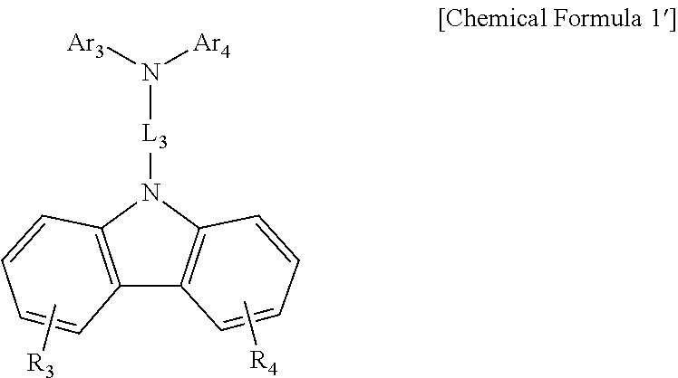
Alternatively, as the hole transport material and the 1-1 host, a compound represented by a following Chemical Formula 1′ may be used:
Figure US11223017-20220111-C00014
in Chemical Formula 1′,
R3 and R4 are each independently hydrogen; deuterium; halogen; nitrile; nitro; amino; a substituted or unsubstituted C1-60 alkyl; a substituted or unsubstituted C3-60 cycloalkyl; a substituted or unsubstituted C2-60 alkenyl; a substituted or unsubstituted C6-60 aryl; or a substituted or unsubstituted C2-60 heterocyclic group containing at least one of O, N, Si and S,
L3 is a bond, or a substituted or unsubstituted C6-60 arylene, and
Ar3 and Ar4 are each independently a substituted or unsubstituted C6-60 aryl; or a substituted or unsubstituted C2-60 heteroaryl containing at least one of O, N, Si and S.
Preferably, R3 and R4 are hydrogen.
Preferably, L3 is biphenylylene.
Preferably, Ar3 and Ar4 are biphenylyl.
Preferably, the compound represented by the Chemical Formula 1′ may be a following compound:
Figure US11223017-20220111-C00015
The preparation method of the compound will be described more specifically in the following Examples.
Also, in addition to the fact that the hole transport material and the 1-1 host included in the first light emitting layer are the same, the 1-2 host included in the first light emitting layer and the 2-1 host included in the second light emitting layer are the same. That is, the hole transport layer, the first light emitting layer and the second light emitting layer are sequentially laminated, and the 1-2 host included in the first light emitting layer and the 2-1 host included in the second light emitting layer use the same material.
As described above, since the first light emitting layer comprises the same material as the hole transport layer, the holes may be sufficiently supplied to the first light emitting layer. However, in order to improve the overall luminous efficiency of the organic light emitting device, the electrons should easily enter the first light emitting layer through the second light emitting layer. To this end, by including the material that the same as the host of the second light emitting layer and different from the hole transport layer of the first light emitting layer, the balance between the electrons and the holes in the first light emitting layer may be appropriately adjusted to increase the luminous efficiency. In addition, when the electrons are injected from the second light emitting layer to the first light emitting layer, the electrons move through the same material, so that the interface resistance between the first light emitting layer and the second light emitting layer is reduced and the driving voltage may be lowered.
As the 1-2 host, a compound represented by a following Chemical Formula 2 may be used:
Figure US11223017-20220111-C00016
in Chemical Formula 2,
Ar5 and Ar6 are each independently a substituted or unsubstituted C6-60 aryl.
Preferably, the compound represented by the Chemical Formula 2 may be any one selected from the group consisting of:
Figure US11223017-20220111-C00017
Figure US11223017-20220111-C00018
Figure US11223017-20220111-C00019
Figure US11223017-20220111-C00020
Figure US11223017-20220111-C00021
Figure US11223017-20220111-C00022
Figure US11223017-20220111-C00023
Figure US11223017-20220111-C00024
The compound represented by the Chemical Formula 2 may be prepared as in following Reaction Formula 2:
Figure US11223017-20220111-C00025
(In Reaction Formula 2, Ar3 and Ar4 are the same as defined in Chemical Formula 2)
Specifically, the compound represented by the Chemical Formula 2 may be prepared by a process including the step of reacting the compound represented by the Chemical Formula 2′ with the compound represented by the Chemical Formula 2″. The preparation method will be described more specifically in the following Examples.
As described above, the first light emitting layer comprises two kinds of hosts, and one of the hosts is the same as the material of the hole transport layer and the other is the same as the second light emitting layer.
Also, the second light emitting layer of the present disclosure may further comprise one kind of the host other than the 2-1 host, that is, the 2-2 host. As the 2-2 host, a compound represented by a following Chemical Formula 3 may be used.
Figure US11223017-20220111-C00026
in Chemical Formula 3,
L4 is a bond; a substituted or unsubstituted C6-60 arylene; or a substituted or unsubstituted C2-60 heteroarylene containing at least one of O, N, Si and S,
Ar7 and Ar8 are each independently a substituted or unsubstituted C6-60 aryl; or a substituted or unsubstituted C2-60 heteroaryl containing at least one of O, N, Si and S, and
Ar9 is a substituted or unsubstituted C2-60 heteroaryl containing at least one N.
Preferably, L4 is phenylene, or dibenzofurandiyl.
Preferably, Ar7 and Ar8 are phenyl.
Preferably, Ar9 is any one selected from the group consisting of:
Figure US11223017-20220111-C00027
Preferably, the compound represented by the Chemical Formula 3 may be any one selected from the group consisting of:
Figure US11223017-20220111-C00028
The preparation method of the compound will be described more specifically in the following Examples.
In the mean time, the first light emitting layer is preferably a red light emitting layer. For this, the first light emitting layer preferably comprises a red phosphorescent dopant. The red phosphorescent dopant is not particularly limited as long as it is a red phosphorescent dopant used in an organic light emitting device. For example, the first light emitting layer may further comprise a compound represented by a following formula 4:
Figure US11223017-20220111-C00029
in Chemical Formula 4,
n1 is 1 or 2,
R5 to R8 are each independently hydrogen; a substituted or unsubstituted C1-60 alkyl; or a substituted or unsubstituted C6-60 aryl; provided that one or more of R5 to R8 are a branched alkyl containing 4 or more carbons, and
X-Y is an auxiliary ligand.
Preferably, n1 is 2.
Preferably, R5 is isobutyl. Preferably, R6 is hydrogen. Preferably, R7 and R8 are methyl.
Preferably, X—Y is acetylacetonate.
Preferably, the compound represented by the Chemical Formula 4 may be a following compound.
Figure US11223017-20220111-C00030
Also, the second light emitting layer is preferably a yellowish green light emitting layer. For this, the second light emitting layer preferably comprises a yellowish green phosphorescent dopant. The yellowish green phosphorescent dopant is not particularly limited as long as it is a yellowish green phosphorescent dopant used in an organic light emitting device. For example,
the second light emitting layer may further comprise a compound represented by a following formula 5:
Figure US11223017-20220111-C00031
in Chemical Formula 5,
n2 is 1 or 2,
a is an integer of 0 to 4, and
Ar10 and Ar11 are each independently a substituted or unsubstituted C6-60 aryl; or a substituted or unsubstituted C2-60 heteroaryl containing at least one of O, N, Si and S.
Preferably, n2 is 2.
Preferably, a is 0.
Preferably, Ar10 and Ar11 are each independently phenyl.
Preferably, the compound represented by the Chemical Formula 5 may be a following compound.
Figure US11223017-20220111-C00032
The Third Light Emitting Layer
The organic light emitting device of the present disclosure may further comprise the third light emitting layer. Preferably, the organic light emitting device of the present disclosure may have a structure that the hole transport layer, the first light emitting layer, the second light emitting layer and the third light emitting layer are sequentially laminated.
Particularly, the third light emitting layer comprises the 3-1 host and the 3-2 host. Further, the same material is used for the 1-2 host, the 2-1 host and the 3-1 host.
The first light emitting layer should have a role of injecting holes and the third light emitting layer should have a role of injecting electrons around the second light emitting layer. As described above, the first light emitting layer contains the same material as the material included in the hole transport layer which is excellent in hole transport. In addition, since the first light emitting layer is farthest from the cathode, it is preferable that the third light emitting layer comprises the same material as the second light emitting layer in order to smoothly provide electrons. Since the second light emitting layer is located closer to the cathode than the first light emitting layer, it is necessary to transport electrons well, but the charge balance may be adjusted to improve efficiency by including a material having bipolar characteristic. Further, since the same material is included in two or more light emitting layers, there is also an effect of lowering the driving voltage by reducing the interfacial resistance between light emitting layers.
In addition, the third light emitting layer of the present disclosure may further comprise one kind of the host other than the 3-1 host, that is, the 3-2 host. As the 3-2 host, a compound represented by a following Chemical Formula 3 may be used.
The 3-2 host may use a compound represented by a following Chemical Formula 3.
Figure US11223017-20220111-C00033
in Chemical Formula 3,
L4 is a bond; a substituted or unsubstituted C6-60 arylene; or a substituted or unsubstituted C2-60 heteroarylene containing at least one of O, N, Si and S,
Ar7 and Ar8 are each independently a substituted or unsubstituted C6-60 aryl; or a substituted or unsubstituted C2-60 heteroaryl containing at least one of O, N, Si and S, and
Ar9 is a substituted or unsubstituted C2-60 heteroaryl containing at least one N.
Preferably, L4 is phenylene, or dibenzofurandiyl.
Preferably, Ar7 and Ar8 are phenyl.
Preferably, Ar9 is any one selected from the group consisting of:
Figure US11223017-20220111-C00034
Preferably, the compound represented by the Chemical Formula 3 may be any one selected from the group consisting of:
Figure US11223017-20220111-C00035
The preparation method of the compound will be described more specifically in the following Examples.
In the mean time, the third light emitting layer is preferably a green light emitting layer. For this, the third light emitting layer preferably comprises a green phosphorescent dopant. The green phosphorescent dopant is not particularly limited as long as it is a green phosphorescent dopant used in an organic light emitting device. For example, the third light emitting layer may further comprise a compound represented by a following Chemical Formula 6:
Figure US11223017-20220111-C00036
in Chemical Formula 6,
n3 is 1 or 2, and
R8 to R11 are each independently hydrogen; deuterium; halogen; nitrile; nitro; amino; a substituted or unsubstituted C1-60 alkyl; a substituted or unsubstituted C3-60 cycloalkyl; a substituted or unsubstituted C2-60 alkenyl; a substituted or unsubstituted C6-60 aryl; or a substituted or unsubstituted C2-60 heterocyclic group containing at least one of O, N, Si and S.
Preferably, n3 is 1.
Preferably, R8 to R11 are each independently hydrogen, or CD3.
Preferably, R8 is hydrogen, and R9 to R11 are CD3.
Preferably, the compound represented by the Chemical Formula 6 may be a following compound.
Figure US11223017-20220111-C00037
The Electron Transport Layer
The electron transport material of the present disclosure is a layer receiving the electrons from the electron injection layer which is formed in or on the cathode, and transporting the electrons to the light emitting layer. For the electron transport material, a material which can receive the electrons well from the cathode and transport the electrons to the light emitting layer, a material having large mobility to the electrons, is suitable.
Specific examples of the electron transport material include an 8-hydroxyquinoline Al complex; a complex including Alq3; an organic radical compound; a hydroxyflavone-metal complex, and the like, but are not limited thereto. The electron transport layer may be used together with a predetermined desired cathode material as used according to the prior art. Particularly, an example of an appropriate cathode material is a general material having the low work function and followed by an aluminum layer or a silver layer. Specific examples thereof include cesium, barium, calcium, ytterbium, and samarium, and each case is followed by the aluminum layer or the silver layer.
The Electron Injection Layer
The organic light emitting device of the present disclosure may further comprise the electron injection layer between the electron transport layer and the cathode. The electron injection layer is a layer injecting the electrons from the electrode, and a compound which has an ability of transporting the electrons, an electron injection effect from the cathode, and an excellent electron injection effect to the light emitting layer or the light emitting material, prevents movement of an exciton generated in the light emitting layer to the hole injection layer, and has an excellent thin film forming ability is preferable.
Specific examples of the material for the electron injection layer include fluorenone, anthraquinodimethane, diphenoquinone, thiopyran dioxide, oxazole, oxadiazole, triazole, imidazole, perylene tetracarboxylic acid, fluorenylidene methane, anthrone, and the like, and derivatives thereof, a metal complex compound, a nitrogen-containing 5-membered cycle derivative, and the like, but are not limited thereto.
Examples of the metal complex compound include 8-hydroxyquinolinato lithium, bis(8-hydroxyquinolinato)zinc, bis(8-hydroxyquinolinato)copper, bis(8-hydroxyquinolinato)manganese, tris(8-hydroxyquinolinato)aluminum, tris(2-methyl-8-hydroxyquinolinato)aluminum, tris(8-hydroxyquinolinato)gallium, bis(10-hydroxybenzo[h]quinolinato)beryllium, bis(10-hydroxybenzo[h]quinolinato)zinc, bis(2-methyl-8-quinolinato)chlorogallium, bis(2-methyl-8-quinolinato)(o-cresolato)gallium, bis(2-methyl-8-quinolinato)(1-naphtholato)aluminum, bis(2-methyl-8-quinolinato)(2-naphtholato)gallium, and the like, but are not limited thereto.
The Organic Light Emitting Device
The structure of the organic light emitting device according to the present disclosure is illustrated in FIG. 1. FIG. 1 illustrates an example of an organic light emitting device including a substrate (1), an anode (2), a hole transport layer (3), a first light emitting layer (4), a second light emitting layer (5), an electron transport layer (6), and a cathode (7).
Also, another structure of the organic light emitting device according to the present disclosure is illustrated in FIG. 2. FIG. 2 illustrates an example of an organic light emitting device including a substrate (1), an anode (2), a hole transport layer (3), a first light emitting layer (4), a second light emitting layer (5), a third light emitting layer (8), an electron transport layer (6) and a cathode (7).
The organic light emitting device according to the present disclosure may be manufactured by sequentially laminating the above mentioned components. In this case, the organic light emitting device may be manufactured by depositing a metal, metal oxides having conductivity, or an alloy thereof on the substrate by using a PVD (physical vapor deposition) method such as a sputtering method or an e-beam evaporation method to form the anode, forming the organic material layer including the hole injection layer, the hole transport layer, the light emitting layer, and the electron transport layer thereon, and then depositing a material which can be used as the cathode thereon. In addition to such a method, the organic light emitting device may be manufactured by sequentially depositing a cathode material, the organic material layer, and an anode material on the substrate. Further, the light emitting layer may be formed using the host and the dopant by a solution coating method as well as a vacuum deposition method. Herein, the solution coating method means spin coating, dip coating, doctor blading, inkjet printing, screen printing, a spray method, roll coating, or the like, but is not limited thereto.
In addition to such a method, the organic light emitting device may be manufactured by sequentially depositing a cathode material, an organic material layer, and an anode material on a substrate (International Publication WO 2003/012890). However, the manufacturing method is not limited thereto.
Meanwhile, the organic light emitting device according to the present disclosure may be a front side emission type, a back side emission type, or a double side emission type according to the used material.
Hereinafter, the preferred Examples are provided for better understanding. However, these Examples are for illustrative purposes only, and the present invention is not intended to be limited by these Examples.
Preparation Example 1
    • 1) Preparation of Compound 1-1
Figure US11223017-20220111-C00038
To the deaerated toluene (500 mL), Compound represented by A (144 mmol), Compound represented by B (111 mmol), tri-tert-butylphosphine (4.4 mmol), palladium acetate (1.1 mmol) and sodium tert-butoxide (166 mmol) were added, and the mixture was heated under reflux for 2 hours. The reaction mixture was cooled down to room temperature, increased with toluene and filtered through celite. The filtrate was evaporated under vacuum and the residue was crystallized from ethyl acetate/heptane. The crude product was extracted from a Soxhlet extractor (toluene) and purified by sublimation under vacuum.
MS: [M+H]+=676
Hereinafter, following compounds were prepared in the same manner as in the preparation of Compound 1-1, except that the Compound represented by A and the Compound represented by B were changed to correspond to the compound structure to be prepared.
2) Preparation of Compound 1-7
Figure US11223017-20220111-C00039
3) Preparation of Compound 1-8
Figure US11223017-20220111-C00040
4) Preparation of Compound 1-13
Figure US11223017-20220111-C00041
Compound represented by A′ (46.6 mmol), Compound represented by B′ (51.3 mmol), potassium carbonate (139.8 mmol) and tetrakis(triphenylphosphine)palladium(0) (0.9 mmol) were added to THF, and the mixture was refluxed for 18 hours. After the reaction was completed, the water layer was removed, the organic layer was dried with magnesium sulfate, and the filtrate was distilled under reduced pressure. The resulting solid was dissolved in chloroform (100 ml), and ethyl acetate (100 ml) was added thereto, followed by recrystallization and drying.
MS: [M+H]+=639
Preparation Example 2
1) Preparation of Compound 2-1
Figure US11223017-20220111-C00042
Compound represented by C (50 mmol), Compound represented by D (55 mmol), K2CO3 (100 mmol), and Pd(PPh3)4 were mixed with THF (200 mL) and H2O (100 mL), followed by stirring and refluxing for about 20 hours. After the reaction mixture was cooled down to room temperature, the water layer was removed and the organic layer was evaporated. The residue was dissolved in toluene and washed with water. After the water layer was removed, the organic layer was evaporated, and the residue was subjected to column chromatography using a silica gel.
MS: [M+H]+=561
Hereinafter, following compounds were prepared in the same manner as in the preparation of Compound 2-1, except that the Compound represented by C and the Compound represented by D were changed to correspond to the compound structure to be prepared.
2) Preparation of Compound 2-2
Figure US11223017-20220111-C00043
3) Preparation of Compound 2-3
Figure US11223017-20220111-C00044
4) Preparation of Compound 2-4
Figure US11223017-20220111-C00045
5) Preparation of Compound 2-5
Figure US11223017-20220111-C00046
6) Preparation of Compound 2-10
Figure US11223017-20220111-C00047
7) Preparation of Compound 2-11
Figure US11223017-20220111-C00048
8) Preparation of Compound 2-12
Figure US11223017-20220111-C00049
9) Preparation of Compound 2-13
Figure US11223017-20220111-C00050
10) Preparation of Compound 2-23
Figure US11223017-20220111-C00051
11) Preparation of the Compound 2-30
Figure US11223017-20220111-C00052
Preparation Example 3
1) Preparation of the Compound 3-1
Figure US11223017-20220111-C00053
Compound represented by E (156 mmol), Compound represented by F (172 mmol), sodium carbonate (340 mmol) were mixed with ethylene glycol diamine ether (1000 mL) and water (280 mL). Tetrakis(triphenylphosphine)palladium(0) (1.5 mmol) was added herein, and the mixture was heated under reflux for 16 hours. After the reaction mixture was cooled down to room temperature, the organic phase was separated, filtered through a silica gel, washed three times with 200 mL of water, and subsequently evaporated. The product was purified using a column chromatography on a silica gel with toluene/heptane (1:2) and sublimed under vacuum.
MS: [M+H]+=641
2) Preparation of Compound 3-2
Figure US11223017-20220111-C00054
Compound represented by G (67 mmol), Compound represented by H (74 mmol), and 19.3 g of NaOtBu were mixed with 1000 mL of p-xylene. And then Pd(OAc)2 (1.34 mmol) and 1 M tri-tert-butylphosphine solution (1 mL) were added to the suspension. The reaction mixture was heated under reflux for 16 hours. After the reaction mixture was cooled down to room temperature, dichloromethane was added thereto, the organic phase was separated, washed three times with 200 mL of water, and then evaporated. The residue was extracted with hot toluene, recrystallized from toluene and finally sublimed under vacuum.
MS: [M+H]+=591
Example 1
The glass substrate on which a thin film of ITO (indium tin oxide) was applied in a thickness of 150 nm was put into distilled water having the detergent dissolved therein and washed by the ultrasonic wave. The used detergent was a product commercially available from Fisher Co. and the distilled water was one which had been twice filtered by using a filter commercially available from Millipore Co. The ITO was washed for 30 minutes, and washing with ultrasonic waves was then repeated twice for 10 minutes by using distilled water. After the washing with distilled water was finished, washing with ultrasonic waves was performed using solvents of isopropyl alcohol, acetone, and methanol. And then the glass substrate was dried, and transported to a plasma scrubber. The substrate was washed using oxygen plasma for 5 minutes, and transported to a vacuum evaporator. And then a following HI-1 compound was thermally deposited under vacuum to a thickness of 50 nm on the ITO transparent electrode prepared above to form a hole injection layer.
And the Compound prepared in Preparation Example 1-1 was thermally deposited under vacuum to form a hole transport layer in a thickness of 100 nm. And then the Compounds prepared in Preparation Example 1-1 and 2-1 (a weight ratio of 7:3) as hosts and a following RD compound (2 wt % based on the host) as a dopant were simultaneously deposited under vacuum to form a first light emitting layer in a thickness of 150 nm. The Compounds prepared in Preparation Example 2-1 and 3-2 (a weight ratio of 3:7) as hosts and a following YGD compound (10 wt % based on the hosts) as a dopant were simultaneously deposited under vacuum to form a second light emitting layer in a thickness of 300 nm. And then the Compounds prepared in Preparation Example 2-1 and 3-2 (a weight ratio of 3:7) as hosts and a following GD compound (5 wt % based on the host) as a dopant were simultaneously deposited under vacuum to form a third light emitting layer in a thickness of 100 nm.
And a following ET2 compound was deposited under vacuum to form an electron transport layer in a thickness of 250 nm. And then a following ET1 compound (lithium doping amount of 2%) was deposited under vacuum to form an electron injection layer in a thickness of 100 nm. And aluminum was deposited to form a cathode, thereby preparing an organic light emitting device.
Figure US11223017-20220111-C00055
Figure US11223017-20220111-C00056
Examples 2 to 23 and Comparative Examples 1 to 8
An organic light emitting device was prepared in the same manner as in Example 1, except that Compounds described in Table 1 and Table 2 below were used as the hole transport layer, the first light emitting layer, the second light emitting layer, and the third light emitting layer. In Table 1 and Table 2, each material means the number of the Preparation Example and the value in parentheses means weight %.
Meanwhile, RH in Table 2 means that a following compound was used.
Figure US11223017-20220111-C00057
TABLE 1
HTL Red Host YG Host Green Host
Example 1 1-1  1-1 (70%) 2-1 (30%) 2-1 (30%) 3-2 (70%) 2-1 (30%) 3-2 (70%)
Example 2 1-7  1-7 (70%) 2-1 (30%) 2-1 (30%) 3-2 (70%) 2-1 (30%) 3-2 (70%)
Example 3 1-8  1-8 (70%) 2-1 (30%) 2-1 (30%) 3-2 (70%) 2-1 (30%) 3-2 (70%)
Example 4 1-13 1-13 (70%) 2-1 (30%) 2-1 (30%) 3-2 (70%) 2-1 (30%) 3-2 (70%)
Example 5 1-13 1-13 (50%) 2-1 (50%) 2-1 (30%) 3-2 (70%) 2-1 (30%) 3-2 (70%)
Example 6 1-13 1-13 (30%) 2-1 (70%) 2-1 (30%) 3-2 (70%) 2-1 (30%) 3-2 (70%)
Example 7 1-13 1-13 (70%) 2-1 (30%) 2-1 (50%) 3-2 (70%) 2-1 (30%) 3-2 (70%)
Example 8 1-13 1-13 (70%) 2-1 (30%) 2-1 (70%) 3-2 (70%) 2-1 (30%) 3-2 (70%)
Example 9 1-13 1-13 (70%) 2-1 (30%) 2-1 (30%) 3-2 (70%) 2-1 (50%) 3-2 (50%)
Example 10 1-13 1-13 (70%) 2-1 (30%) 2-1 (30%) 3-2 (70%) 2-1 (70%) 3-2 (30%)
Example 11 1-1  1-1 (70%) 2-2 (30%) 2-2 (30%) 3-2 (70%) 2-2 (30%) 3-2 (70%)
Example 12 1-7  1-7 (70%) 2-3 (30%) 2-3 (30%) 3-2 (70%) 2-3 (30%) 3-2 (70%)
Example 13 1-13 1-13 (70%) 2-4 (30%) 2-4 (30%) 3-2 (70%) 2-4 (30%) 3-2 (70%)
Example 14 1-1  1-1 (70%) 2-5 (30%) 2-5 (30%) 3-2 (70%) 2-5 (30%) 3-2 (70%)
Example 15 1-7  1-7 (70%) 2-10 (30%)  2-10 (30%)  3-2 (70%) 2-10 (30%)  3-2 (70%)
Example 16 1-13 1-13 (70%) 2-11 (30%)  2-11 (30%)  3-2 (70%) 2-11 (30%)  3-2 (70%)
Example 17 1-1  1-1 (70%) 2-12 (30%)  2-12 (30%)  3-2 (70%) 2-12 (30%)  3-2 (70%)
Example 18 1-7  1-7 (70%) 2-13 (30%)  2-13 (30%)  3-2 (70%) 2-13 (30%)  3-2 (70%)
Example 19 1-13 1-13 (70%) 2-23 (30%)  2-23 (30%)  3-2 (70%) 2-23 (30%)  3-2 (70%)
Example 20 1-1  1-1 (70%) 2-30 (30%)  2-30 (30%)  3-2 (70%) 2-30 (30%)  3-2 (70%)
Example 21 1-1  1-1 (70%) 2-1 (30%) 2-1 (30%) 3-1 (70%) 2-1 (30%) 3-1 (70%)
Example 22 1-7  1-7 (70%) 2-1 (30%) 2-1 (30%) 3-1 (70%) 2-1 (30%) 3-2 (70%)
Example 23 1-13 1-13 (70%) 2-1 (30%) 2-1 (30%) 3-2 (70%) 2-1 (30%) 3-1 (70%)
TABLE 2
HTL Red Host YG Host Green Host
Comparative 1-1 RH (100%) 3-1 (100%) 3-2 (100%)
Example 1
Comparative 1-7 RH (50%) 2-1 (50%) 2-1 (30%) 3-1 (70%) 2-1 (30%) 3-2 (70%)
Example 2
Comparative 1-8 RH (50%) 2-1 (50%) 2-1 (30%) 3-2 (70%) 2-1 (30%) 3-1 (70%)
Example 3
Comparative  1-13 RH (50%) 2-2 (50%) 2-4 (30%) 3-1 (70%) 2-4 (30%) 3-1 (70%)
Example 4
Comparative 1-1 1-1 (70%) 2-5 (30%) 2-30 (30%)  3-1 (70%) 2-30 (30%)  3-1 (70%)
Example 5
Comparative 1-7 1-7 (70%) 2-12 (30%)  2-5 (30%) 3-2 (70%) 2-5 (30%) 3-2 (70%)
Example 6
Comparative 1-8 1-8 (70%) 2-5 (30%) 2-10 (30%)  3-1 (70%) 2-10 (30%)  3-1 (70%)
Example 7
Comparative  1-13 1-13 (70%) 2-11 (30%)  2-23 (30%)  3-2 (70%) 2-23 (30%)  3-2 (70%)
Example 8
Experimental Example 1
Currents were applied to the organic light emitting devices prepared in Examples 1 to 23 and Comparative Examples 1 to 8 to obtain the results shown in Table 3 and Table 4 below.
TABLE 3
@10 mA/cm2 @100 mA/cm2
V Cd/A CIE_x CIE_y LT (95%) hours
Example 1 5.72 61.87 0.428 0.557 177
Example 2 5.21 60.02 0.447 0.540 163
Example 3 4.84 60.27 0.469 0.520 187
Example 4 5.01 56.12 0.481 0.509 152
Example 5 5.22 58.04 0.487 0.503 160
Example 6 4.94 55.32 0.491 0.503 147
Example 7 5.37 59.36 0.494 0.500 175
Example 8 5.52 60.18 0.469 0.497 179
Example 9 4.84 60.27 0.443 0.520 165
Example 10 4.44 66.98 0.467 0.543 166
Example 11 5.00 68.73 0.440 0.523 146
Example 12 4.60 72.81 0.487 0.546 170
Example 13 5.13 54.22 0.477 0.503 164
Example 14 5.15 61.62 0.482 0.514 148
Example 15 5.13 56.44 0.486 0.508 149
Example 16 4.89 56.46 0.476 0.504 152
Example 17 5.18 55.45 0.486 0.514 168
Example 18 5.05 59.82 0.481 0.505 172
Example 19 5.02 56.12 0.487 0.509 159
Example 20 5.21 52.54 0.478 0.503 157
Example 21 5.17 58.53 0.478 0.512 177
Example 22 4.89 56.48 0.478 0.512 143
Example 23 3.66 63.47 0.490 0.503 173
TABLE 4
@10 mA/cm2 @100 mA/cm2
V Cd/A CIE_x CIE_y LT (95%) hours
Comparative 5.72 38.59 0.513 0.479 121
Example 1
Comparative 5.72 37.89 0.517 0.475 109
Example 2
Comparative 5.92 36.57 0.521 0.475 87
Example 3
Comparative 5.88 35.78 0.524 0.469 93
Example 4
Comparative 5.79 36.45 0.520 0.472 108
Example 5
Comparative 6.12 35.51 0.524 0.468 127
Example 6
Comparative 6.03 37.28 0.519 0.473 114
Example 7
Comparative 5.87 37.70 0.514 0.478 76
Example 8
Example 24
The glass substrate on which a thin film of ITO (indium tin oxide) was applied in a thickness of 150 nm was put into distilled water having the detergent dissolved therein and washed by the ultrasonic wave. The used detergent was a product commercially available from Fisher Co. and the distilled water was one which had been twice filtered by using a filter commercially available from Millipore Co. The ITO was washed for 30 minutes, and washing with ultrasonic waves was then repeated twice for 10 minutes by using distilled water. After the washing with distilled water was finished, washing with ultrasonic waves was performed using solvents of isopropyl alcohol, acetone, and methanol. And then the glass substrate was dried, and transported to a plasma scrubber. The substrate was washed using oxygen plasma for 5 minutes, and then transported to a vacuum evaporator. The HI-1 compound was thermally deposited under vacuum to a thickness of 50 nm on the ITO transparent electrode prepared above to form a hole injection layer.
And the Compound prepared in Preparation Example 1-1 was thermally deposited under vacuum to form a hole transport layer in a thickness of 100 nm. And then the Compounds prepared in Preparation Example 1-1 and 2-1 (a weight ratio of 7:3) as hosts and the RD compound (2 wt % based on the host) as a dopant were simultaneously deposited under vacuum to form a first light emitting layer in a thickness of 100 nm. The Compounds prepared in Preparation Example 2-1 and 3-2 (a weight ratio of 3:7) as hosts and the YGD compound (10 wt % based on the hosts) as a dopant were simultaneously deposited under vacuum to form a second light emitting layer in a thickness of 400 nm.
And the ET2 compound was deposited under vacuum to form an electron transport layer in a thickness of 250 nm. And then the ET1 compound (lithium doping amount of 2%) was deposited under vacuum to form an electron injection layer in a thickness of 100 nm. And aluminum was deposited to form a cathode, thereby preparing an organic light emitting device.
Examples 25 to 43 and Comparative Examples 9 to 16
An organic light emitting device was prepared in the same manner as in Example 24, except that Compounds described in Table 5 and Table 6 below were used as the hole transport layer, the first light emitting layer, and the second light emitting layer. In Table 5 and Table 6, each material means the number of the Preparation Example and the value in parentheses means weight %.
TABLE 5
HTL Red Host YG Host
Example 1-1 1-1 (70%) 2-1 (30%) 2-1 (30%) 3-2 (70%)
24
Example 1-7 1-7 (70%) 2-1 (30%) 2-1 (30%) 3-2 (70%)
25
Example 1-8 1-8 (70%) 2-1 (30%) 2-1 (30%) 3-2 (70%)
26
Example 1-13 1-13 (70%)  2-1 (30%) 2-1 (30%) 3-2 (70%)
27
Example 1-13 1-13 (50%)  2-1 (50%) 2-1 (30%) 3-2 (70%)
28
Example 1-13 1-13 (30%)  2-1 (70%) 2-1 (30%) 3-2 (70%)
29
Example 1-13 1-13 (70%)  2-1 (30%) 2-1 (50%) 3-2 (50%)
30
Example 1-13 1-13 (70%)  2-1 (30%) 2-1 (70%) 3-2 (30%)
31
Example 1-1 1-1 (70%) 2-2 (30%) 2-2 (30%) 3-1 (70%)
32
Example 1-7 1-7 (70%) 2-3 (30%) 2-3 (30%) 3-1 (70%)
33
Example 1-13 1-13 (70%)  2-4 (30%) 2-4 (30%) 3-1 (70%)
34
Example 1-1 1-1 (70%) 2-5 (30%) 2-5 (30%) 3-1 (70%)
35
Example 1-7 1-7 (70%) 2-10 (30%)  2-10 (30%)  3-1 (70%)
36
Example 1-13 1-13 (70%)  2-11 (30%)  2-11 (30%)  3-1 (70%)
37
Example 1-1 1-1 (70%) 2-12 (30%)  2-12 (30%)  3-2 (70%)
38
Example 1-7 1-7 (70%) 2-13 (30%)  2-13 (30%)  3-1 (70%)
39
Example 1-13 1-13 (70%)  2-23 (30%)  2-23 (30%)  3-2 (70%)
40
Example 1-1 1-1 (70%) 2-30 (30%)  2-30 (30%)  3-1 (70%)
41
Example 1-7 1-7 (70%) 2-1 (30%) 2-1 (30%) 3-1 (70%)
42
Example 1-13 1-13 (70%)  2-1 (30%) 2-1 (30%) 3-1 (70%)
43
TABLE 6
HTL Red Host YG Host
Comparative 1-1 RH (100%) 3-1 (100%)
Example 9
Comparative 1-7 RH (50%) 2-30 (50%)  2-30 (30%) 3-1 (70%)
Example 10
Comparative 1-8 RH (50%) 2-23 (50%)  2-13 (30%) 3-2 (70%)
Example 11
Comparative 1-13 RH (50%) 2-11 (50%)  2-12 (30%) 3-1 (70%)
Example 12
Comparative 1-1 1-1 (70%) 2-5 (30%) 2-10 (30%) 3-1 (70%)
Example 13
Comparative 1-7 1-7 (70%) 2-4 (30%)  2-4 (30%) 3-2 (70%)
Example 14
Comparative 1-8 1-8 (70%) 2-1 (30%) 2-13 (30%) 3-1 (70%)
Example 15
Comparative 1-13 1-13 (70%)  2-2 (30%) 2-23 (30%) 3-2 (70%)
Example 16
Experimental Example 2
Currents were applied to the organic light emitting devices prepared in Examples 24 to 43 and Comparative Examples 9 to 16 to obtain the results shown in Table 7 and Table 8 below.
TABLE 7
@10 mA/cm2 @100 mA/cm2
V Cd/A CIE_x CIE_y LT (95%) hours
Example 24 3.92 56.28 0.497 0.496 125
Example 25 3.80 58.79 0.493 0.500 127
Example 26 3.94 59.70 0.499 0.494 132
Example 27 4.03 57.65 0.498 0.495 119
Example 28 3.90 60.56 0.495 0.499 121
Example 29 3.98 60.94 0.497 0.496 110
Example 30 3.92 65.37 0.495 0.498 134
Example 31 4.15 65.38 0.500 0.493 132
Example 32 4.04 66.11 0.496 0.497 147
Example 33 3.91 61.76 0.495 0.498 137
Example 34 3.93 61.03 0.498 0.496 132
Example 35 4.05 60.10 0.500 0.494 140
Example 36 4.05 57.41 0.501 0.492 119
Example 37 3.92 59.38 0.498 0.495 125
Example 38 3.98 56.63 0.500 0.493 138
Example 39 4.15 63.31 0.502 0.491 141
Example 40 4.09 64.69 0.500 0.493 123
Example 41 3.99 60.82 0.499 0.494 128
Example 42 3.99 59.15 0.498 0.495 132
Example 43 4.02 58.45 0.499 0.494 132
TABLE 8
@10 mA/cm2 @100 mA/cm2
V Cd/A CIE_x CIE_y LT (95%) hours
Comparative 4.02 40.56 0.493 0.499 72
Example 9
Comparative 4.02 38.19 0.493 0.499 77
Example 10
Comparative 4.03 36.97 0.494 0.499 53
Example 11
Comparative 4.03 35.83 0.496 0.496 65
Example 12
Comparative 4.05 37.99 0.526 0.468 21
Example 13
Comparative 4.01 39.17 0.507 0.486 76
Example 14
Comparative 4.03 45.89 0.513 0.481 80
Example 15
Comparative 4.04 45.49 0.521 0.472 55
Example 16
DESCRIPTION OF SYMBOLS
1: substrate 2: anode
3: hole transport layer 4: first light emitting layer
5: second light emitting layer 6: electron transport layer
7: cathode 8: anode

Claims (13)

The invention claimed is:
1. An organic light emitting device comprising:
a first electrode;
a hole transport layer;
a first light emitting layer;
a second light emitting layer;
a third light emitting layer;
an electron transport layer; and
a second electrode,
wherein the first light emitting layer comprises a 1-1 host and a 1-2 host,
the second light emitting layer comprises a 2-1 host and a 2-2 host,
the hole transport layer comprises the same material as the 1-1 host,
the 1-1 host and the 2-2 host are different materials from each other,
wherein the third light emitting layer is disposed between the second light emitting layer and the electron transport layer, and comprises a 3-1 host and a 3-2 host,
the 1-2 host, the 2-1 host and the 3-1 host are the same materials, and
wherein the 1-2 host is a compound represented by Chemical Formula 2:
Figure US11223017-20220111-C00058
in Chemical Formula 2,
Ar5 and Ar6 are each independently a substituted or unsubstituted C6-60 aryl.
2. The organic light emitting device of claim 1,
wherein the 1-1 host is a compound represented by Chemical Formula 1:
Figure US11223017-20220111-C00059
in Chemical Formula 1,
R1 and R2 are each independently hydrogen; deuterium; halogen; nitrile; nitro; amino; a substituted or unsubstituted C1-60 alkyl; a substituted or unsubstituted C3-60 cycloalkyl; a substituted or unsubstituted C2-60 alkenyl; a substituted or unsubstituted C6-60 aryl; or a substituted or unsubstituted C2-60 heterocyclic group containing at least one of 0, N, Si and S,
L1 and L2 are each independently a bond, or a substituted or unsubstituted C6-60 arylene, and
Ar1 and Ar2 are each independently a substituted or unsubstituted C6-60 aryl; or a substituted or unsubstituted C2-60 heteroaryl containing at least one of 0, N, Si and S.
3. The organic light emitting device of claim 2,
wherein the compound represented by the Chemical Formula 1 is any one selected from the group consisting of:
Figure US11223017-20220111-C00060
Figure US11223017-20220111-C00061
Figure US11223017-20220111-C00062
Figure US11223017-20220111-C00063
4. The organic light emitting device of claim 1,
wherein the 1-1 host is a compound represented by Chemical Formula 1′:
Figure US11223017-20220111-C00064
in Chemical Formula 1′,
R3 and R4 are each independently hydrogen; deuterium; halogen; nitrile; nitro; amino; a substituted or unsubstituted C1-60 alkyl; a substituted or unsubstituted C3-60 cycloalkyl; a substituted or unsubstituted C2-60 alkenyl; a substituted or unsubstituted C6-60 aryl; or a substituted or unsubstituted C2-60 heterocyclic group containing at least one of 0, N, Si and S,
L3 is a bond, or a substituted or unsubstituted C6-60 arylene, and
Ar3 and Ar4 are each independently a substituted or unsubstituted C6-60 aryl; or a substituted or unsubstituted C2-60 heteroaryl containing at least one of 0, N, Si and S.
5. The organic light emitting device of claim 4,
wherein the compound represented by the Chemical Formula 1′ is a following compound:
Figure US11223017-20220111-C00065
6. The organic light emitting device of claim 1,
wherein the compound represented by the Chemical Formula 2 is any one selected from the group consisting of:
Figure US11223017-20220111-C00066
Figure US11223017-20220111-C00067
Figure US11223017-20220111-C00068
Figure US11223017-20220111-C00069
Figure US11223017-20220111-C00070
Figure US11223017-20220111-C00071
Figure US11223017-20220111-C00072
Figure US11223017-20220111-C00073
7. The organic light emitting device of claim 1,
wherein the 2-2 host is a compound represented by Chemical Formula 3:
Figure US11223017-20220111-C00074
in Chemical Formula 3,
L4 is a bond; a substituted or unsubstituted C6-60 arylene; or a substituted or unsubstituted C2-60 heteroarylene containing at least one of 0, N, Si and S,
Ar7 and Ar8 are each independently a substituted or unsubstituted C6-60 aryl; or a substituted or unsubstituted C2-60 heteroaryl containing at least one of 0, N, Si and S, and
Ar9 is a substituted or unsubstituted C2-60 heteroaryl containing at least one N.
8. The organic light emitting device of claim 7,
wherein the compound represented by the Chemical Formula 3 is any one selected from the group consisting of:
Figure US11223017-20220111-C00075
9. The organic light emitting device of claim 2,
wherein the 3-2 host is a compound represented by Chemical Formula 3:
Figure US11223017-20220111-C00076
in Chemical Formula 3,
L4 is a bond; a substituted or unsubstituted C6-60 arylene; or a substituted or unsubstituted C2-60 heteroarylene containing at least one of O, N, Si and S,
Ar7 and Ar8 are each independently a substituted or unsubstituted C6-60 aryl; or a substituted or unsubstituted C2-60 heteroaryl containing at least one of O, N, Si and S, and
Ar9 is a substituted or unsubstituted C2-60 heteroaryl containing at least one N.
10. The organic light emitting device of claim 9,
wherein the compound represented by the Chemical Formula 3 is any one selected from the group consisting of:
Figure US11223017-20220111-C00077
11. The organic light emitting device of claim 1,
wherein the first light emitting layer further comprises a compound represented by Chemical Formula 4:
Figure US11223017-20220111-C00078
in Chemical Formula 4,
n1 is 1 or 2,
R5 to R8 are each independently hydrogen; a substituted or unsubstituted C1-60 alkyl; or a substituted or unsubstituted C6-60 aryl; provided that one or more of R5 to R8 are a branched alkyl containing 4 or more carbons, and
X—Y is an auxiliary ligand.
12. The organic light emitting device of claim 1,
wherein the second light emitting layer further comprises a compound represented by Chemical Formula 5:
Figure US11223017-20220111-C00079
in Chemical Formula 5,
n2 is 1 or 2,
a is an integer of 0 to 4, and
Ar10 and Ar11 are each independently a substituted or unsubstituted C6-60 aryl; or a substituted or unsubstituted C2-60 heteroaryl containing at least one of O, N, Si and S.
13. The organic light emitting device of claim 2,
wherein the third light emitting layer further comprises a compound represented by Chemical Formula 6:
Figure US11223017-20220111-C00080
in Chemical Formula 6,
n3 is 1 or 2, and
R8 to R11 are each independently hydrogen; deuterium; halogen; nitrile; nitro; amino; a substituted or unsubstituted C1-60 alkyl; a substituted or unsubstituted C3-60 cycloalkyl; a substituted or unsubstituted C2-60 alkenyl; a substituted or unsubstituted C6-60 aryl; or a substituted or unsubstituted C2-60 heterocyclic group containing at least one of O, N, Si and S.
US15/744,508 2016-09-06 2017-06-26 Organic light emitting device Active 2039-04-01 US11223017B2 (en)

Applications Claiming Priority (3)

Application Number Priority Date Filing Date Title
KR1020160114284A KR101744248B1 (en) 2016-09-06 2016-09-06 Organic light emitting device
KR10-2016-0114284 2016-09-06
PCT/KR2017/006722 WO2018048074A1 (en) 2016-09-06 2017-06-26 Organic light-emitting element

Publications (2)

Publication Number Publication Date
US20190006590A1 US20190006590A1 (en) 2019-01-03
US11223017B2 true US11223017B2 (en) 2022-01-11

Family

ID=59223310

Family Applications (1)

Application Number Title Priority Date Filing Date
US15/744,508 Active 2039-04-01 US11223017B2 (en) 2016-09-06 2017-06-26 Organic light emitting device

Country Status (7)

Country Link
US (1) US11223017B2 (en)
EP (1) EP3336159B1 (en)
JP (1) JP6598173B2 (en)
KR (1) KR101744248B1 (en)
CN (1) CN108064258B (en)
TW (1) TWI640115B (en)
WO (1) WO2018048074A1 (en)

Families Citing this family (34)

* Cited by examiner, † Cited by third party
Publication number Priority date Publication date Assignee Title
KR101744248B1 (en) 2016-09-06 2017-06-07 주식회사 엘지화학 Organic light emitting device
KR101885898B1 (en) * 2016-11-16 2018-08-06 주식회사 엘지화학 Organic light emitting device
KR102008897B1 (en) 2017-06-22 2019-10-23 삼성에스디아이 주식회사 Organic optoelectronic device and display device
KR101947747B1 (en) * 2018-05-04 2019-02-13 삼성에스디아이 주식회사 Compound for organic optoelectronic device, composition for organic optoelectronic device and organic optoelectronic device and display device
US20190198772A1 (en) 2017-06-22 2019-06-27 Samsung Sdi Co., Ltd. Compound for organic optoelectronic device, composition for organic optoelectronic device and organic optoelectronic device and display deivce
KR102717279B1 (en) * 2017-07-05 2024-10-15 메르크 파텐트 게엠베하 Composition for organic electronic devices
KR102075251B1 (en) * 2017-07-07 2020-02-07 주식회사 엘지화학 Novel compound and organic light emitting device comprising the same
KR102118629B1 (en) * 2017-07-14 2020-06-03 주식회사 엘지화학 Organic light emitting device
KR102107085B1 (en) * 2017-07-14 2020-05-06 주식회사 엘지화학 Organic light emitting device
KR101856728B1 (en) 2017-08-10 2018-05-10 주식회사 엘지화학 Organic light emitting device
KR101959821B1 (en) * 2017-09-15 2019-03-20 엘티소재주식회사 Organic light emitting device, manufacturing method of the same and composition for organic layer of organic light emitting device
TWI785142B (en) * 2017-11-14 2022-12-01 德商麥克專利有限公司 Composition for organic electronic devices
KR102134383B1 (en) * 2017-12-12 2020-07-15 주식회사 엘지화학 Organic light emitting device
CN111868050B (en) * 2017-12-21 2023-07-25 广州华睿光电材料有限公司 Composition for preparing organic electronic device, organic electronic device and application
WO2019120085A1 (en) * 2017-12-21 2019-06-27 广州华睿光电材料有限公司 Printing ink comprising thermally activated delayed fluorescent material and application thereof
WO2019120177A1 (en) * 2017-12-21 2019-06-27 广州华睿光电材料有限公司 Compound for manufacturing organic display device, organic display device and application thereof
JP7102211B2 (en) * 2018-04-26 2022-07-19 キヤノン株式会社 Organic EL element, display device having it, lighting device, moving body
KR102231624B1 (en) 2018-09-04 2021-03-24 주식회사 엘지화학 Organic light emitting device
CN110903321B (en) * 2018-09-15 2023-12-12 北京夏禾科技有限公司 Fluorine-substituted metal complexes
KR102702683B1 (en) 2018-12-28 2024-09-03 엘지디스플레이 주식회사 Organic light emitting diode and organic light emitting device including the same
US11542252B2 (en) 2018-12-28 2023-01-03 Samsung Electronics Co., Ltd. Heterocyclic compound, composition including the same, and organic light-emitting device including the heterocyclic compound
US11739081B2 (en) * 2019-03-11 2023-08-29 Universal Display Corporation Organic electroluminescent materials and devices
CN112640148B (en) * 2019-05-02 2024-02-06 株式会社Lg化学 organic light emitting devices
US12517088B2 (en) 2019-05-15 2026-01-06 Lg Chem, Ltd. Method for selecting material for organic light-emitting device
WO2021040278A1 (en) * 2019-08-26 2021-03-04 주식회사 엘지화학 Organic light-emitting device
US20230026162A1 (en) 2019-10-11 2023-01-26 Idemitsu Kosan Co.,Ltd. Compound, material for organic electroluminescent element, organic electroluminescent element, and electronic device
KR20210063747A (en) 2019-11-25 2021-06-02 삼성전자주식회사 Organometallic compound, organic light emitting device including the same and a composition for diagnosing including the same
KR102400109B1 (en) * 2019-12-10 2022-05-19 주식회사 엘지화학 Organic light emitting device
EP4118695B1 (en) 2020-03-11 2024-05-01 Merck Patent GmbH Organic electroluminescent apparatus
KR20220151193A (en) 2020-03-11 2022-11-14 메르크 파텐트 게엠베하 organic electroluminescent device
CN111554821B (en) 2020-05-14 2023-10-24 京东方科技集团股份有限公司 Organic electroluminescent device, display panel and display device
KR20220043755A (en) 2020-09-29 2022-04-05 삼성전자주식회사 Organometallic compound, organic light emitting device including the same and electronic apparatus including the organic light emitting device
EP4002509A1 (en) 2020-11-20 2022-05-25 Samsung Electronics Co., Ltd. Light-emitting device and electronic apparatus including the same
CN114628601B (en) * 2020-12-11 2024-10-15 北京夏禾科技有限公司 Organic electroluminescent device

Citations (34)

* Cited by examiner, † Cited by third party
Publication number Priority date Publication date Assignee Title
KR20000051826A (en) 1999-01-27 2000-08-16 성재갑 New organomattalic complex molecule for the fabrication of organic light emitting diodes
WO2003012890A2 (en) 2001-07-20 2003-02-13 Novaled Gmbh Light emitting component with organic layers
US20040183082A1 (en) 2003-03-17 2004-09-23 Hiroko Yamazaki Light emitting element and light emitting device
US20050233166A1 (en) 2004-04-14 2005-10-20 Eastman Kodak Company OLED device using reduced drive voltage
US20100301312A1 (en) * 2007-12-21 2010-12-02 Idemitsu Kosan Co., Ltd. Organic electroluminescence device
US20110057178A1 (en) 2009-09-04 2011-03-10 Semiconductor Energy Laboratory, Co., Ltd. Light-Emitting Element, Light-Emitting Device, and Method for Manufacturing the Same
US20110108810A1 (en) 2009-11-10 2011-05-12 Canon Kabushiki Kaisha Organic electroluminescence device
US20130026452A1 (en) * 2011-07-28 2013-01-31 Universal Display Corporation Heteroleptic iridium complexes as dopants
US20130126831A1 (en) * 2011-11-21 2013-05-23 Universal Display Corporation Organic light emitting materials
US20130146850A1 (en) 2011-12-08 2013-06-13 Lg Display Co., Ltd. Tandem White Organic Light Emitting Device
US20130207046A1 (en) * 2010-09-15 2013-08-15 Merck Patent Gmbh Materials for organic electroluminescent devices
US20130240933A1 (en) 2012-03-14 2013-09-19 Semiconductor Energy Laboratory Co., Ltd. Light-Emitting Element, Light-Emitting Device, Display Device, Electronic Device, and Lighting Device
TW201339123A (en) 2012-02-14 2013-10-01 Merck Patent Gmbh Material for organic electroluminescent device
US8604689B2 (en) 2010-11-11 2013-12-10 Nitto Denko Corporation Hybrid composite emissive construct and light-emitting devices using the same
US20140042469A1 (en) 2012-08-10 2014-02-13 Semiconductor Energy Laboratory Co., Ltd. Light-Emitting Element, Light-Emitting Device, Display Device, Electronic Device, and Lighting Device
CN103620808A (en) 2011-06-24 2014-03-05 出光兴产株式会社 Organic electroluminescent element
US20140145168A1 (en) 2012-11-29 2014-05-29 Semiconductor Energy Laboratory Co., Ltd. Light-Emitting Element, Light-Emitting Device, Electronic Device, and Lighting Device
US20140340888A1 (en) 2013-05-17 2014-11-20 Semiconductor Energy Laboratory Co., Ltd. Light-emitting element, lighting device, light-emitting device, and electronic device
US20150097161A1 (en) 2013-10-04 2015-04-09 Lg Display Co., Ltd. Organic light emitting device and organic light emitting display having the same
US20150155511A1 (en) 2013-12-02 2015-06-04 Semiconductor Energy Laboratory Co., Ltd. Light-emitting element, display module, lighting module, light-emitting device, display device, electronic appliance, and lighting device
US20150243905A1 (en) * 2012-06-14 2015-08-27 Idemitsu Kosan Co., Ltd. Biscarbazole derivative host materials and green emitter for oled emissive region
KR20150111014A (en) 2014-03-24 2015-10-05 엘지디스플레이 주식회사 White Organic Light Emitting Device
WO2015169412A1 (en) * 2014-05-05 2015-11-12 Merck Patent Gmbh Materials for organic light emitting devices
KR20150128590A (en) 2014-05-08 2015-11-18 롬엔드하스전자재료코리아유한회사 An electron transport material and an organic electroluminescence device comprising the same
KR20150138000A (en) 2014-05-30 2015-12-09 제일모직주식회사 Organic optoelectric device and display device
US20150364696A1 (en) 2014-06-13 2015-12-17 Samsung Display Co., Ltd. Organic light-emitting device and method of manufacturing the same
WO2016013875A1 (en) 2014-07-22 2016-01-28 Rohm And Haas Electronic Materials Korea Ltd. Organic electroluminescent device
KR20160011582A (en) 2014-07-22 2016-02-01 롬엔드하스전자재료코리아유한회사 Organic Electroluminescence Device
KR20160024625A (en) 2014-08-26 2016-03-07 삼성에스디아이 주식회사 Organic optoelectric device and display device
KR20160027940A (en) 2014-09-02 2016-03-10 주식회사 엘지화학 Organic light emitting device
US20160111644A1 (en) 2014-10-17 2016-04-21 Samsung Display Co., Ltd. Organic light-emitting device
KR20160078317A (en) 2013-09-30 2016-07-04 주식회사 엘지화학 Heterocyclic compound and organic light emitting device comprising the same
KR20160095319A (en) 2015-02-03 2016-08-11 덕산네오룩스 주식회사 Organic electronic element, and an electronic device comprising the same
KR101744248B1 (en) 2016-09-06 2017-06-07 주식회사 엘지화학 Organic light emitting device

Family Cites Families (1)

* Cited by examiner, † Cited by third party
Publication number Priority date Publication date Assignee Title
TWI685128B (en) * 2013-10-16 2020-02-11 日商半導體能源研究所股份有限公司 Light-emitting element, light-emitting device, electronic device, and lighting device

Patent Citations (53)

* Cited by examiner, † Cited by third party
Publication number Priority date Publication date Assignee Title
KR20000051826A (en) 1999-01-27 2000-08-16 성재갑 New organomattalic complex molecule for the fabrication of organic light emitting diodes
WO2003012890A2 (en) 2001-07-20 2003-02-13 Novaled Gmbh Light emitting component with organic layers
US7274141B2 (en) 2001-07-20 2007-09-25 Novaled Gmbh Inverted organic light emitting diode with doped layers
US20040183082A1 (en) 2003-03-17 2004-09-23 Hiroko Yamazaki Light emitting element and light emitting device
CN102738410A (en) 2003-03-17 2012-10-17 株式会社半导体能源研究所 Light emitting element and light emitting device
US20050233166A1 (en) 2004-04-14 2005-10-20 Eastman Kodak Company OLED device using reduced drive voltage
CN1943057A (en) 2004-04-14 2007-04-04 伊斯曼柯达公司 Oled device using reduced drive voltage
US20100301312A1 (en) * 2007-12-21 2010-12-02 Idemitsu Kosan Co., Ltd. Organic electroluminescence device
US20110057178A1 (en) 2009-09-04 2011-03-10 Semiconductor Energy Laboratory, Co., Ltd. Light-Emitting Element, Light-Emitting Device, and Method for Manufacturing the Same
CN102484923A (en) 2009-09-04 2012-05-30 株式会社半导体能源研究所 Light-emitting element, light-emitting device, and method for manufacturing the same
US20110108810A1 (en) 2009-11-10 2011-05-12 Canon Kabushiki Kaisha Organic electroluminescence device
CN102082234A (en) 2009-11-10 2011-06-01 佳能株式会社 Organic electroluminescence device
US20130207046A1 (en) * 2010-09-15 2013-08-15 Merck Patent Gmbh Materials for organic electroluminescent devices
JP5972894B2 (en) 2010-11-11 2016-08-17 日東電工株式会社 Hybrid composite light-emitting structure and light-emitting device using the same
US8604689B2 (en) 2010-11-11 2013-12-10 Nitto Denko Corporation Hybrid composite emissive construct and light-emitting devices using the same
CN103620808A (en) 2011-06-24 2014-03-05 出光兴产株式会社 Organic electroluminescent element
US20140217378A1 (en) 2011-06-24 2014-08-07 Idemitsu Kosan Co., Ltd. Organic electroluminescent element
US20130026452A1 (en) * 2011-07-28 2013-01-31 Universal Display Corporation Heteroleptic iridium complexes as dopants
US20130126831A1 (en) * 2011-11-21 2013-05-23 Universal Display Corporation Organic light emitting materials
US20130146850A1 (en) 2011-12-08 2013-06-13 Lg Display Co., Ltd. Tandem White Organic Light Emitting Device
CN103165817A (en) 2011-12-08 2013-06-19 乐金显示有限公司 Tandem white organic light emitting device
KR20140133572A (en) 2012-02-14 2014-11-19 메르크 파텐트 게엠베하 Spirobifluorene compounds for organic electroluminescent devices
US20150065730A1 (en) * 2012-02-14 2015-03-05 Merck Patent Gmbh Spirobifluorene compounds for organic electroluminescent devices
TW201339123A (en) 2012-02-14 2013-10-01 Merck Patent Gmbh Material for organic electroluminescent device
TW201401602A (en) 2012-03-14 2014-01-01 Semiconductor Energy Lab Light-emitting element, light-emitting device, display device, electronic device, and lighting device
US20130240933A1 (en) 2012-03-14 2013-09-19 Semiconductor Energy Laboratory Co., Ltd. Light-Emitting Element, Light-Emitting Device, Display Device, Electronic Device, and Lighting Device
US20150243905A1 (en) * 2012-06-14 2015-08-27 Idemitsu Kosan Co., Ltd. Biscarbazole derivative host materials and green emitter for oled emissive region
JP2014056814A (en) 2012-08-10 2014-03-27 Semiconductor Energy Lab Co Ltd Light-emitting element, light-emitting device, display device, electronic apparatus and light device
US20140042469A1 (en) 2012-08-10 2014-02-13 Semiconductor Energy Laboratory Co., Ltd. Light-Emitting Element, Light-Emitting Device, Display Device, Electronic Device, and Lighting Device
US20140145168A1 (en) 2012-11-29 2014-05-29 Semiconductor Energy Laboratory Co., Ltd. Light-Emitting Element, Light-Emitting Device, Electronic Device, and Lighting Device
US20140340888A1 (en) 2013-05-17 2014-11-20 Semiconductor Energy Laboratory Co., Ltd. Light-emitting element, lighting device, light-emitting device, and electronic device
CN104167494A (en) 2013-05-17 2014-11-26 株式会社半导体能源研究所 Light-emitting element, lighting device, light-emitting device, and electronic device
KR20160078317A (en) 2013-09-30 2016-07-04 주식회사 엘지화학 Heterocyclic compound and organic light emitting device comprising the same
US20150097161A1 (en) 2013-10-04 2015-04-09 Lg Display Co., Ltd. Organic light emitting device and organic light emitting display having the same
KR20150040118A (en) 2013-10-04 2015-04-14 엘지디스플레이 주식회사 Organic emitting device and organic emitting display device comprising the same
US20150155511A1 (en) 2013-12-02 2015-06-04 Semiconductor Energy Laboratory Co., Ltd. Light-emitting element, display module, lighting module, light-emitting device, display device, electronic appliance, and lighting device
KR20150111014A (en) 2014-03-24 2015-10-05 엘지디스플레이 주식회사 White Organic Light Emitting Device
WO2015169412A1 (en) * 2014-05-05 2015-11-12 Merck Patent Gmbh Materials for organic light emitting devices
US20170186965A1 (en) * 2014-05-05 2017-06-29 Merck Patent Gmbh Materials for organic light emitting devices
KR20150128590A (en) 2014-05-08 2015-11-18 롬엔드하스전자재료코리아유한회사 An electron transport material and an organic electroluminescence device comprising the same
US20170077415A1 (en) 2014-05-08 2017-03-16 Rohm And Haas Electronic Materials Korea Ltd. An electron transport material and an organic electroluminescence device comprising the same
KR20150138000A (en) 2014-05-30 2015-12-09 제일모직주식회사 Organic optoelectric device and display device
KR20150143963A (en) 2014-06-13 2015-12-24 삼성디스플레이 주식회사 Organic light-emitting devices and method for manufacturing the same
US20150364696A1 (en) 2014-06-13 2015-12-17 Samsung Display Co., Ltd. Organic light-emitting device and method of manufacturing the same
WO2016013875A1 (en) 2014-07-22 2016-01-28 Rohm And Haas Electronic Materials Korea Ltd. Organic electroluminescent device
KR20160011582A (en) 2014-07-22 2016-02-01 롬엔드하스전자재료코리아유한회사 Organic Electroluminescence Device
US20170207396A1 (en) 2014-07-22 2017-07-20 Rohm And Haas Electronic Materials Korea Ltd. Organic electroluminescent device
KR20160024625A (en) 2014-08-26 2016-03-07 삼성에스디아이 주식회사 Organic optoelectric device and display device
KR20160027940A (en) 2014-09-02 2016-03-10 주식회사 엘지화학 Organic light emitting device
US20160111644A1 (en) 2014-10-17 2016-04-21 Samsung Display Co., Ltd. Organic light-emitting device
KR20160046075A (en) 2014-10-17 2016-04-28 삼성디스플레이 주식회사 Organic light-emitting devices
KR20160095319A (en) 2015-02-03 2016-08-11 덕산네오룩스 주식회사 Organic electronic element, and an electronic device comprising the same
KR101744248B1 (en) 2016-09-06 2017-06-07 주식회사 엘지화학 Organic light emitting device

Non-Patent Citations (4)

* Cited by examiner, † Cited by third party
Title
LEE SUNGHUN; LIMBACH DANIEL; KIM KWON-HYEON; YOO SEUNG-JUN; PARK YOUNG-SEO; KIM JANG-JOO: "High efficiency and non-color-changing orange organic light emitting diodes with red and green emitting layers", ORGANIC ELECTRONICS, ELSEVIER, AMSTERDAM, NL, vol. 14, no. 7, 25 April 2013 (2013-04-25), AMSTERDAM, NL, pages 1856 - 1860, XP028554618, ISSN: 1566-1199, DOI: 10.1016/j.orgel.2013.04.020
Lee, et al.: "High efficiency and non-color-changing orange organic light emitting diodes with red and green emitting layers", XP28554618, Organic Electronics, Elsevier, vol. 14, No. 7, Apr. 25, 2013, pp. 1856-1860.
Zhao et al.: "A hybrid white organic light-emitting diode with stable color and reduced efficiency roll-off by using a bipolar charge carrier switch", XP28856897, Organic Electronics, Elsevier, vol. 13, No. 6, Mar. 10, 2012, pp. 11049-1055.
ZHAO FANGCHAO; ZHANG ZHIQIANG; LIU YIPENG; DAI YANFENG; CHEN JIANGSHAN; MA DONGGE: "A hybrid white organic light-emitting diode with stable color and reduced efficiency roll-off by using a bipolar charge carrier switch", ORGANIC ELECTRONICS, ELSEVIER, AMSTERDAM, NL, vol. 13, no. 6, 10 March 2012 (2012-03-10), AMSTERDAM, NL, pages 1049 - 1055, XP028856897, ISSN: 1566-1199, DOI: 10.1016/j.orgel.2012.03.005

Also Published As

Publication number Publication date
EP3336159A1 (en) 2018-06-20
TW201813155A (en) 2018-04-01
WO2018048074A1 (en) 2018-03-15
CN108064258A (en) 2018-05-22
KR101744248B1 (en) 2017-06-07
US20190006590A1 (en) 2019-01-03
JP2018531480A (en) 2018-10-25
JP6598173B2 (en) 2019-10-30
TWI640115B (en) 2018-11-01
EP3336159A4 (en) 2018-10-10
EP3336159B1 (en) 2019-08-28
CN108064258B (en) 2020-04-14

Similar Documents

Publication Publication Date Title
US11223017B2 (en) Organic light emitting device
CN107840835B (en) New Heterocyclic Compounds and Organic Light-Emitting Elements Using The Same
US10454056B1 (en) Organic light emitting device
US20210391544A1 (en) Cyclic compound and organic light emitting device comprising same
US11700768B2 (en) Compound and organic light emitting device comprising the same
JP6801162B2 (en) New heterocyclic compounds and organic light emitting devices using them
US11515478B2 (en) Compound and organic light emitting device using the same
EP3546453B1 (en) Novel heterocyclic compound and organic light emitting element using same
US20190058131A1 (en) Organic light emitting device
KR102069310B1 (en) Novel hetero-cyclic compound and organic light emitting device comprising the same
US12010912B2 (en) Heterocyclic compound and organic light emitting device comprising the same
KR102280260B1 (en) Novel hetero-cyclic compound and organic light emitting device comprising the same
US10833278B2 (en) Compound and organic light emitting device comprising the same
US11795161B2 (en) Compound and organic light emitting device comprising same
KR102576227B1 (en) Novel compound and organic light emitting device comprising the same
US9960357B2 (en) Spiro-type compound and organic light emitting element comprising same
KR102538111B1 (en) Novel compound and organic light emitting device comprising the same
KR102258617B1 (en) Novel hetero-cyclic compound and organic light emitting device comprising the same
EP3747873B1 (en) Novel compound and organic light emitting diode using same
US20240292744A1 (en) Compound and organic light emitting device comprising the same
US12202838B2 (en) Heterocyclic compound and organic light emitting device comprising same
KR20210074048A (en) Novel amine-based compound and organic light emitting device comprising the same
KR20210049477A (en) Novel amine-based compound and organic light emitting device comprising the same
US12391678B2 (en) Compound and organic light emitting device comprising same
US20250120310A1 (en) Compound and organic light emitting device comprising the same

Legal Events

Date Code Title Description
AS Assignment

Owner name: LG CHEM, LTD., KOREA, REPUBLIC OF

Free format text: ASSIGNMENT OF ASSIGNORS INTEREST;ASSIGNORS:PARK, TAE YOON;JEON, SANG YOUNG;CHUN, MIN SEUNG;AND OTHERS;REEL/FRAME:044610/0900

Effective date: 20171102

FEPP Fee payment procedure

Free format text: ENTITY STATUS SET TO UNDISCOUNTED (ORIGINAL EVENT CODE: BIG.); ENTITY STATUS OF PATENT OWNER: LARGE ENTITY

STPP Information on status: patent application and granting procedure in general

Free format text: DOCKETED NEW CASE - READY FOR EXAMINATION

STPP Information on status: patent application and granting procedure in general

Free format text: NON FINAL ACTION MAILED

STPP Information on status: patent application and granting procedure in general

Free format text: FINAL REJECTION MAILED

STPP Information on status: patent application and granting procedure in general

Free format text: DOCKETED NEW CASE - READY FOR EXAMINATION

STPP Information on status: patent application and granting procedure in general

Free format text: NON FINAL ACTION COUNTED, NOT YET MAILED

STPP Information on status: patent application and granting procedure in general

Free format text: NON FINAL ACTION MAILED

STPP Information on status: patent application and granting procedure in general

Free format text: RESPONSE TO NON-FINAL OFFICE ACTION ENTERED AND FORWARDED TO EXAMINER

STPP Information on status: patent application and granting procedure in general

Free format text: AWAITING TC RESP., ISSUE FEE NOT PAID

STPP Information on status: patent application and granting procedure in general

Free format text: NOTICE OF ALLOWANCE MAILED -- APPLICATION RECEIVED IN OFFICE OF PUBLICATIONS

STPP Information on status: patent application and granting procedure in general

Free format text: PUBLICATIONS -- ISSUE FEE PAYMENT VERIFIED

STCF Information on status: patent grant

Free format text: PATENTED CASE

MAFP Maintenance fee payment

Free format text: PAYMENT OF MAINTENANCE FEE, 4TH YEAR, LARGE ENTITY (ORIGINAL EVENT CODE: M1551); ENTITY STATUS OF PATENT OWNER: LARGE ENTITY

Year of fee payment: 4