US11222983B2 - Display substrate, manufacturing method thereof, and display device - Google Patents
Display substrate, manufacturing method thereof, and display device Download PDFInfo
- Publication number
- US11222983B2 US11222983B2 US16/825,999 US202016825999A US11222983B2 US 11222983 B2 US11222983 B2 US 11222983B2 US 202016825999 A US202016825999 A US 202016825999A US 11222983 B2 US11222983 B2 US 11222983B2
- Authority
- US
- United States
- Prior art keywords
- doped region
- ohmic contact
- lightly doped
- base substrate
- orthographic projection
- Prior art date
- Legal status (The legal status is an assumption and is not a legal conclusion. Google has not performed a legal analysis and makes no representation as to the accuracy of the status listed.)
- Active
Links
Images


Classifications
-
- H—ELECTRICITY
- H10—SEMICONDUCTOR DEVICES; ELECTRIC SOLID-STATE DEVICES NOT OTHERWISE PROVIDED FOR
- H10D—INORGANIC ELECTRIC SEMICONDUCTOR DEVICES
- H10D30/00—Field-effect transistors [FET]
- H10D30/60—Insulated-gate field-effect transistors [IGFET]
- H10D30/67—Thin-film transistors [TFT]
- H10D30/6729—Thin-film transistors [TFT] characterised by the electrodes
- H10D30/6737—Thin-film transistors [TFT] characterised by the electrodes characterised by the electrode materials
-
- G—PHYSICS
- G02—OPTICS
- G02F—OPTICAL DEVICES OR ARRANGEMENTS FOR THE CONTROL OF LIGHT BY MODIFICATION OF THE OPTICAL PROPERTIES OF THE MEDIA OF THE ELEMENTS INVOLVED THEREIN; NON-LINEAR OPTICS; FREQUENCY-CHANGING OF LIGHT; OPTICAL LOGIC ELEMENTS; OPTICAL ANALOGUE/DIGITAL CONVERTERS
- G02F1/00—Devices or arrangements for the control of the intensity, colour, phase, polarisation or direction of light arriving from an independent light source, e.g. switching, gating or modulating; Non-linear optics
- G02F1/01—Devices or arrangements for the control of the intensity, colour, phase, polarisation or direction of light arriving from an independent light source, e.g. switching, gating or modulating; Non-linear optics for the control of the intensity, phase, polarisation or colour
- G02F1/13—Devices or arrangements for the control of the intensity, colour, phase, polarisation or direction of light arriving from an independent light source, e.g. switching, gating or modulating; Non-linear optics for the control of the intensity, phase, polarisation or colour based on liquid crystals, e.g. single liquid crystal display cells
- G02F1/133—Constructional arrangements; Operation of liquid crystal cells; Circuit arrangements
- G02F1/1333—Constructional arrangements; Manufacturing methods
- G02F1/1343—Electrodes
- G02F1/134309—Electrodes characterised by their geometrical arrangement
-
- H01L29/78618—
-
- H—ELECTRICITY
- H10—SEMICONDUCTOR DEVICES; ELECTRIC SOLID-STATE DEVICES NOT OTHERWISE PROVIDED FOR
- H10D—INORGANIC ELECTRIC SEMICONDUCTOR DEVICES
- H10D30/00—Field-effect transistors [FET]
- H10D30/60—Insulated-gate field-effect transistors [IGFET]
- H10D30/67—Thin-film transistors [TFT]
- H10D30/6704—Thin-film transistors [TFT] having supplementary regions or layers in the thin films or in the insulated bulk substrates for controlling properties of the device
- H10D30/6713—Thin-film transistors [TFT] having supplementary regions or layers in the thin films or in the insulated bulk substrates for controlling properties of the device characterised by the properties of the source or drain regions, e.g. compositions or sectional shapes
-
- G—PHYSICS
- G02—OPTICS
- G02F—OPTICAL DEVICES OR ARRANGEMENTS FOR THE CONTROL OF LIGHT BY MODIFICATION OF THE OPTICAL PROPERTIES OF THE MEDIA OF THE ELEMENTS INVOLVED THEREIN; NON-LINEAR OPTICS; FREQUENCY-CHANGING OF LIGHT; OPTICAL LOGIC ELEMENTS; OPTICAL ANALOGUE/DIGITAL CONVERTERS
- G02F1/00—Devices or arrangements for the control of the intensity, colour, phase, polarisation or direction of light arriving from an independent light source, e.g. switching, gating or modulating; Non-linear optics
- G02F1/01—Devices or arrangements for the control of the intensity, colour, phase, polarisation or direction of light arriving from an independent light source, e.g. switching, gating or modulating; Non-linear optics for the control of the intensity, phase, polarisation or colour
- G02F1/13—Devices or arrangements for the control of the intensity, colour, phase, polarisation or direction of light arriving from an independent light source, e.g. switching, gating or modulating; Non-linear optics for the control of the intensity, phase, polarisation or colour based on liquid crystals, e.g. single liquid crystal display cells
- G02F1/133—Constructional arrangements; Operation of liquid crystal cells; Circuit arrangements
- G02F1/136—Liquid crystal cells structurally associated with a semi-conducting layer or substrate, e.g. cells forming part of an integrated circuit
- G02F1/1362—Active matrix addressed cells
- G02F1/1368—Active matrix addressed cells in which the switching element is a three-electrode device
-
- H01L27/1222—
-
- H01L27/127—
-
- H—ELECTRICITY
- H10—SEMICONDUCTOR DEVICES; ELECTRIC SOLID-STATE DEVICES NOT OTHERWISE PROVIDED FOR
- H10D—INORGANIC ELECTRIC SEMICONDUCTOR DEVICES
- H10D30/00—Field-effect transistors [FET]
- H10D30/01—Manufacture or treatment
- H10D30/021—Manufacture or treatment of FETs having insulated gates [IGFET]
- H10D30/031—Manufacture or treatment of FETs having insulated gates [IGFET] of thin-film transistors [TFT]
- H10D30/0312—Manufacture or treatment of FETs having insulated gates [IGFET] of thin-film transistors [TFT] characterised by the gate electrodes
- H10D30/0316—Manufacture or treatment of FETs having insulated gates [IGFET] of thin-film transistors [TFT] characterised by the gate electrodes of lateral bottom-gate TFTs comprising only a single gate
-
- H—ELECTRICITY
- H10—SEMICONDUCTOR DEVICES; ELECTRIC SOLID-STATE DEVICES NOT OTHERWISE PROVIDED FOR
- H10D—INORGANIC ELECTRIC SEMICONDUCTOR DEVICES
- H10D30/00—Field-effect transistors [FET]
- H10D30/01—Manufacture or treatment
- H10D30/021—Manufacture or treatment of FETs having insulated gates [IGFET]
- H10D30/031—Manufacture or treatment of FETs having insulated gates [IGFET] of thin-film transistors [TFT]
- H10D30/0321—Manufacture or treatment of FETs having insulated gates [IGFET] of thin-film transistors [TFT] comprising silicon, e.g. amorphous silicon or polysilicon
-
- H—ELECTRICITY
- H10—SEMICONDUCTOR DEVICES; ELECTRIC SOLID-STATE DEVICES NOT OTHERWISE PROVIDED FOR
- H10D—INORGANIC ELECTRIC SEMICONDUCTOR DEVICES
- H10D30/00—Field-effect transistors [FET]
- H10D30/60—Insulated-gate field-effect transistors [IGFET]
- H10D30/67—Thin-film transistors [TFT]
- H10D30/6729—Thin-film transistors [TFT] characterised by the electrodes
- H10D30/673—Thin-film transistors [TFT] characterised by the electrodes characterised by the shapes, relative sizes or dispositions of the gate electrodes
- H10D30/6732—Bottom-gate only TFTs
-
- H—ELECTRICITY
- H10—SEMICONDUCTOR DEVICES; ELECTRIC SOLID-STATE DEVICES NOT OTHERWISE PROVIDED FOR
- H10D—INORGANIC ELECTRIC SEMICONDUCTOR DEVICES
- H10D30/00—Field-effect transistors [FET]
- H10D30/60—Insulated-gate field-effect transistors [IGFET]
- H10D30/67—Thin-film transistors [TFT]
- H10D30/674—Thin-film transistors [TFT] characterised by the active materials
- H10D30/6741—Group IV materials, e.g. germanium or silicon carbide
- H10D30/6743—Silicon
- H10D30/6745—Polycrystalline or microcrystalline silicon
-
- H—ELECTRICITY
- H10—SEMICONDUCTOR DEVICES; ELECTRIC SOLID-STATE DEVICES NOT OTHERWISE PROVIDED FOR
- H10D—INORGANIC ELECTRIC SEMICONDUCTOR DEVICES
- H10D62/00—Semiconductor bodies, or regions thereof, of devices having potential barriers
- H10D62/10—Shapes, relative sizes or dispositions of the regions of the semiconductor bodies; Shapes of the semiconductor bodies
- H10D62/13—Semiconductor regions connected to electrodes carrying current to be rectified, amplified or switched, e.g. source or drain regions
- H10D62/149—Source or drain regions of field-effect devices
- H10D62/151—Source or drain regions of field-effect devices of IGFETs
-
- H—ELECTRICITY
- H10—SEMICONDUCTOR DEVICES; ELECTRIC SOLID-STATE DEVICES NOT OTHERWISE PROVIDED FOR
- H10D—INORGANIC ELECTRIC SEMICONDUCTOR DEVICES
- H10D86/00—Integrated devices formed in or on insulating or conducting substrates, e.g. formed in silicon-on-insulator [SOI] substrates or on stainless steel or glass substrates
- H10D86/01—Manufacture or treatment
- H10D86/021—Manufacture or treatment of multiple TFTs
- H10D86/0221—Manufacture or treatment of multiple TFTs comprising manufacture, treatment or patterning of TFT semiconductor bodies
-
- H—ELECTRICITY
- H10—SEMICONDUCTOR DEVICES; ELECTRIC SOLID-STATE DEVICES NOT OTHERWISE PROVIDED FOR
- H10D—INORGANIC ELECTRIC SEMICONDUCTOR DEVICES
- H10D86/00—Integrated devices formed in or on insulating or conducting substrates, e.g. formed in silicon-on-insulator [SOI] substrates or on stainless steel or glass substrates
- H10D86/40—Integrated devices formed in or on insulating or conducting substrates, e.g. formed in silicon-on-insulator [SOI] substrates or on stainless steel or glass substrates characterised by multiple TFTs
- H10D86/421—Integrated devices formed in or on insulating or conducting substrates, e.g. formed in silicon-on-insulator [SOI] substrates or on stainless steel or glass substrates characterised by multiple TFTs having a particular composition, shape or crystalline structure of the active layer
-
- H—ELECTRICITY
- H10—SEMICONDUCTOR DEVICES; ELECTRIC SOLID-STATE DEVICES NOT OTHERWISE PROVIDED FOR
- H10D—INORGANIC ELECTRIC SEMICONDUCTOR DEVICES
- H10D86/00—Integrated devices formed in or on insulating or conducting substrates, e.g. formed in silicon-on-insulator [SOI] substrates or on stainless steel or glass substrates
- H10D86/40—Integrated devices formed in or on insulating or conducting substrates, e.g. formed in silicon-on-insulator [SOI] substrates or on stainless steel or glass substrates characterised by multiple TFTs
- H10D86/60—Integrated devices formed in or on insulating or conducting substrates, e.g. formed in silicon-on-insulator [SOI] substrates or on stainless steel or glass substrates characterised by multiple TFTs wherein the TFTs are in active matrices
-
- H—ELECTRICITY
- H10—SEMICONDUCTOR DEVICES; ELECTRIC SOLID-STATE DEVICES NOT OTHERWISE PROVIDED FOR
- H10K—ORGANIC ELECTRIC SOLID-STATE DEVICES
- H10K59/00—Integrated devices, or assemblies of multiple devices, comprising at least one organic light-emitting element covered by group H10K50/00
- H10K59/10—OLED displays
- H10K59/12—Active-matrix OLED [AMOLED] displays
Definitions
- the present disclosure relates to the field of display technology, and more particularly to a display substrate, a manufacturing method, thereof, and a display device.
- TFT thin-film transistor
- Embodiments of the present disclosure provide a display substrate, a manufacturing method thereof, and a display device.
- an embodiment of the present disclosure provides a display substrate, comprising a base substrate and thin-film transistors disposed on the base substrate, where
- the thin-film transistors each comprises a gate, an active layer insulated from the gate, and two ohmic contact parts in direct contact with the active layer, leaving a gap region between the two ohmic contact parts;
- each of the ohmic contact parts comprises a lightly doped region and a heavily doped region, and an orthographic projection of the lightly doped region on the base substrate and an orthographic projection of the heavily doped region on the base substrate do not overlap each other.
- an orthographic projection of the gate on the base substrate and the orthographic projection of the heavily doped region on the base substrate have an overlapping region.
- the lightly doped region comprises a first lightly doped region, which is located at a side of the heavily doped region away from the center of the active layer.
- an orthographic projection of the first lightly doped region on the base substrate and the orthographic projection of the gate on the base substrate do not overlap each other.
- an orthographic projection of the first lightly doped region on the base substrate and the orthographic projection of the gate on the base substrate have an overlapping region.
- the lightly doped region further comprises a second lightly doped region, which is located at a side of the heavily doped region close to the center of the active layer.
- a doping concentration of the first lightly doped region is same as that of the second lightly doped region.
- the thin-film transistor further includes a source and a drain
- an orthographic projection of the source on the base substrate covers an orthographic projection of one of the ohmic contact parts on the base substrate, and the source is in direct contact with the one of the ohmic contact parts;
- an orthographic projection of the drain on the base substrate covers an orthographic projection of the other of the ohmic contact parts on the base substrate, and the drain is in direct contact with the other one of the ohmic contact parts.
- the two ohmic contact parts in the thin-film transistor are symmetrically disposed with respect to the center of the active layer.
- the ohmic contact parts are made of an N-type semiconductor material.
- an embodiment of the present disclosure provides a manufacturing method of the aforementioned display substrate, including:
- ohmic contact layer on the pattern of the active layer, and performing doping on the ohmic contact layer to form a lightly doped region and a heavily doped region, where an orthographic projection of the lightly doped region on the base substrate and an orthographic projection of the heavily doped region on the base substrate do not overlap each other; and patterning the ohmic contact layer.
- the method further includes:
- performing doping on the ohmic contact parts includes:
- performing doping on the ohmic contact layer includes:
- the method further includes:
- patterning the ohmic contact layer comprises:
- etching the ohmic contact layer by using patterns of the source and drain as a shield, and etching a portion of the active layer.
- an embodiment of the present disclosure provides a display device.
- the display device includes the aforementioned display substrate.
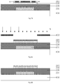
- FIG. 1 is a schematic structural diagram of a display substrate according to an embodiment of the present disclosure
- FIG. 2 is another schematic structural diagram of a display substrate according to an embodiment of the present disclosure
- FIG. 3 is yet another schematic structural diagram of a display substrate according to an embodiment of the present disclosure.
- FIG. 4 is a schematic flow diagram of a manufacturing method of a display substrate according to an embodiment of the present disclosure
- FIG. 5 is a schematic structural diagram of a display substrate with a gate formed according to an implementation of the present disclosure
- FIG. 6 is a schematic structural diagram of a display substrate with an active layer formed according to an embodiment of the present disclosure
- FIGS. 7A to 7D are respective schematic structural diagrams corresponding to respective steps in a doping method according to an embodiment of the present disclosure.
- FIGS. 8A to 8C are respective schematic structural diagrams corresponding to respective steps in another doping method according to an embodiment of the present disclosure.
- FIG. 9 is a schematic structural diagram of a display substrate with a source and a drain formed according to an embodiment of the present disclosure.
- FIG. 10 is a schematic structural diagram after patterning of ohmic contact parts according to an embodiment of the present disclosure.
- embodiments of the present disclosure provide a display substrate, a manufacturing method thereof, and a display device.
- an embodiment of the present disclosure provides a display substrate, as shown in FIG. 1 , including a base substrate 101 and thin-film transistors 102 disposed on the base substrate 101 , where:
- the thin-film transistors 102 each includes a gate 201 , an active layer 202 insulated from the gate, and two ohmic contact parts 203 in direct contact with the active layer 202 , leaving a gap region between the two ohmic contact parts 203 ;
- each of the ohmic contact parts 203 includes a lightly doped region A 1 and a heavily doped region A 2 , and an orthographic projection of the lightly doped region A 1 on the base substrate 101 and an orthographic projection of the heavily doped region A 2 on the base substrate 101 do not overlap each other.
- the entire ohmic contact part is heavily doped, such that the leakage current of the thin-film transistor is increased, which, if serious, can affect the display quality.
- the ohmic contact part is divided into a lightly doped region and a heavily doped region, where a doping concentration of the lightly doped region is less than that of the heavily doped region. Due to the presence of the lightly doped region, a carrier concentration of the thin-film transistor can be reduced, thereby reducing the leakage current and improving the display quality.
- the heavily doped region is provided in the ohmic contact part to allow a good contact between the active layer and a source (or drain).
- providing the lightly doped region in the ohmic contact part is approximate to increasing the channel length which also reduces the leakage current to some extent, so that an input image can be maintained to the arrival of the next signal, and good display of the display substrate is ensured.
- the aforementioned display substrate provided in the embodiment of the present disclosure may be applied to a liquid crystal display device, and the aforementioned thin-film transistor may be a driving transistor; and the display substrate may also be applied to an organic electroluminescent display device, and the aforementioned thin-film transistor may also be a switching transistor.
- the type of the thin-film transistor is not limited here.
- a display substrate may have a plurality of thin-film transistors, and the number of thin-film transistor(s) is not limited here.
- an orthographic projection of the gate 201 on the base substrate 101 and the orthographic projection of the heavily doped region A 2 on the base substrate 101 have an overlapping region.
- the orthographic projection of the heavily doped region A 2 of the ohmic contact part 203 on the base substrate 101 and the orthographic projection of the gate 201 on the base substrate 101 have an overlapping region, and the gate 201 can shield light emitted from a side of the base substrate 101 toward the interior of the display substrate, such as light a and light b in the figure, so the heavily doped region A 2 of the ohmic contact part 203 is not irradiated by the light incident from the side of the base substrate 101 to produce photo-generated carriers.
- the photo-generated carriers generated due to irradiation of the lightly doped region A 1 by the light emitted from the side of the base substrate 101 toward the interior of the display substrate can be reduced, thereby reducing the leakage current.
- the active layer 202 can be fabricated by using MLA (Micro Lens Array) technology.
- MLA Micro Lens Array
- the MLA technology refers to superposition of a plurality of sets of micro lenses to achieve the laser emergence with a high energy density.
- the active layer is formed on a gate insulating layer 206 by using amorphous silicon (a-Si), and the active layer is crystallized by using a mask formed by superposition of a plurality of sets of micro lenses, to cause melting and recrystallization at places irradiated by a laser beam, so that a channel region of the thin-film transistor is selectively converted from amorphous silicon to polysilicon (p-Si) to improve the mobility of the active layer.
- a-Si amorphous silicon
- the lightly doped region A 1 includes a first lightly doped region B 1 , here the first lightly doped region B 1 is located at a side of the heavily doped region A 2 away from the center of the active layer 202 .
- the first lightly doped region B 1 is located at the side of the heavily doped region A 2 away from the center of the active layer 202 , for example, the first lightly doped region B 1 is disposed on the left side of the left-side ohmic contact part 203 or on the right side of the right-side ohmic contact part 203 in the figure, it can be seen obviously from FIG. 1 that the ohmic contact part 203 has a larger contact area with the source 204 (or the drain 205 ) at the outer side as compared with the lightly doped region A 1 of the ohmic contact part 203 provided in other region.
- providing the first lightly doped region B 1 on the side of the ohmic contact part 203 away from the center of the active layer 202 can increase the area ratio of the first lightly doped region in the ohmic contact part, and correspondingly reduce the area ratio of the heavily doped region in the ohmic contact part, so that the leakage current can be further reduced.
- an orthographic projection of the first lightly doped region B 1 on the base substrate 101 and the orthographic projection of the gate 201 on the base substrate 101 do not overlap each other.
- an overlapped area of the orthographic projection of the heavily doped region A 2 on the base substrate 101 and the orthographic projection of the gate 201 on the base substrate 101 can be increased, and the light irradiated from the side of the base substrate 101 to the heavily doped region A 2 can be reduced, thereby reducing the leakage current.
- the orthographic projection of the first lightly doped region B 1 on the base substrate 101 and the orthographic projection of the gate 201 on the base substrate 101 have an overlapping region.
- the orthographic projection of the gate 201 on the base substrate 101 can cover the orthographic projection of the heavily doped region A 2 on the base substrate 101 . Due to the shielding by the gate 201 , the light from the side of the base substrate 101 is not irradiated on the heavily doped region A 2 , so as to reduce the leakage current.
- this arrangement can increase the area ratio of the lightly doped region A 1 in the ohmic contact part 203 , correspondingly reduce the area ratio of the heavily doped region A 2 in the ohmic contact part 203 , and further reduce the leakage current of the thin-film transistor.
- the lightly doped region A 1 further includes a second lightly doped region B 2 , and the second lightly doped region B 2 is located at a side of the heavily doped region A 2 close to the center of the active layer.
- the area ratio of the lightly doped region in the ohmic contact part can be further increased, thereby reducing the leakage current. Furthermore, by providing the second lightly doped region in the ohmic contact part, the channel length is further increased, and the leakage current is further reduced, so that the input image can be maintained to the arrival of the next signal, and good display of the display substrate is ensured.
- the second lightly doped region B 2 can be disposed on a side of the heavily doped region A 2 close to the center of the active layer 202 ; that is, in the lightly doped region consisting of the first lightly doped region B 1 and the second lightly doped region B 2 , a portion can be shielded by the gate 201 , and the other portion is not shielded by the gate 201 , so that the area of the first lightly doped region not shielded by the gate can be maximized, and the leakage current is effectively reduced.
- the first lightly doped region and the second lightly doped region may be formed by the same process; that is, a doping concentration of the first lightly doped region is same as that of the second lightly doped region.
- the first lightly doped region and the second lightly doped region may also be formed by different processes, so that the doping concentration of the first lightly doped region is different from that of the second lightly doped region. This can be selected according to actual needs, and is not specifically limited here.
- the thin-film transistor 102 further includes a source 204 and a drain 205 .
- the orthographic projection of the source 204 on the base substrate 101 covers an orthographic projection of one of the ohmic contact parts 203 on the base substrate 101 , and the source is in direct contact with the ohmic contact part 203 ;
- the orthographic projection of the drain 205 on the base substrate 101 covers an orthographic projection of the other of the ohmic contact parts 203 on the base substrate 101 , and the drain is in direct contact with the ohmic contact part 203 .
- the two ohmic contact parts can be symmetrically disposed with respect to the center of the active layer.
- positions of the first lightly doped regions in the two ohmic contact parts can be set symmetrically, and positions of the second lightly doped regions in the two ohmic contact parts can be set symmetrically.
- the carrier concentration distribution in the two ohmic contact parts can be substantially same, so that the thin-film transistor has better performance.
- ohmic contact part 203 also includes a heavily doped region other than the first lightly doped region B 1 and the second lightly doped region B 2 to ensure a good contact between the active layer and the source (or drain).
- the aforementioned ohmic contact part is an N-type semiconductor material.
- the type of the ohmic contact part can be determined according to actual needs.
- the ohmic contact part may also be a P-type semiconductor material, which is not limited herein.
- an embodiment of the present disclosure provides a manufacturing method of the aforementioned display substrate.
- the problem-solving principle of the manufacturing method is similar to that of the aforementioned display substrate, and thus for the implementation of the manufacturing method, reference can be made to the implementation of the aforementioned display substrate, and repeated description is omitted.
- An embodiment of the present disclosure provides a manufacturing method of the aforementioned display substrate, as shown in FIG. 4 , including:
- doping is performed on the ohmic contact parts to form a lightly doped region in addition to a heavily doped region in each ohmic contact part. Therefore, the number of photo-generated carriers generated under the action of light irradiation or an electric field is smaller, so that the carriers emitted to the drain are reduced, and the leakage current can be effectively reduced. Furthermore, this also increases the channel length, and also reduces the leakage current to some extent, so that the input image can be maintained to the arrival of the next signal, and good display of the display substrate is ensured.
- the method before the above step S 301 , the method further includes: as shown in FIG. 5 , forming a pattern of a gate 201 on the base substrate 101 , and as shown in FIG. 6 , forming a gate insulation layer 206 on a layer where the gate 201 is located.
- the active layer is formed on the gate insulating layer 206 by using amorphous silicon (a-Si), and the active layer is crystallized by using a mask formed by superposition of a plurality of sets of micro lenses, to cause melting and recrystallization at places irradiated by a laser beam, so that a channel region of the thin-film transistor is selectively converted from amorphous silicon to polysilicon (p-Si) to improve the mobility of the active layer.
- a-Si amorphous silicon
- p-Si polysilicon
- the method in the aforementioned manufacturing method provided in the embodiment of the present disclosure, in the above step S 302 , while performing doping on the ohmic contact parts to form a lightly doped region, the method can further includes:
- the first lightly doped region and the second lightly doped region are formed at the same time, so that one doping process can be omitted, and the manufacturing cost is saved.
- the ohmic contact layer 203 can be made of amorphous silicon material, and the pattern of the ohmic contact layer 203 formed on the pattern of the active layer 202 is consistent with the pattern of the active layer 202 , to prevent the subsequent doping process from affecting the active layer 202 .
- performing doping on the ohmic contact parts can include:
- the ohmic contact layer 203 is shielded by a mask 103 , and lightly doped to obtain a structure shown in FIG. 7B , that is, forming a first lightly doped region B 1 and a second lightly doped region B 2 ;
- the ohmic contact layer 203 is shielded by a mask 103 and doped to obtain a structure shown in FIG. 7D , and form a heavily doped region in the regions of the ohmic contact layer 203 except for the first lightly doped region B 1 and the second lightly doped region B 2 .
- the ohmic contact layer may also be doped by the following steps, including:
- regions except for the ohmic contact layer 203 are shielded by a mask 103 to perform light doping on the ohmic contact layer 203 , to obtain a structure shown in FIG. 8B ; and shielding the first lightly doped region B 1 and the second lightly doped region B 2 of the ohmic contact layer 203 , and performing heavy doping on the ohmic contact layer 203 , as shown in FIG. 8C , the ohmic contact part is shielded by a mask 103 and heavily doped to obtain a structure shown in FIG. 7D .
- the method can further include:
- the above step S 303 can include:
- the ohmic contact part is etched by using the source and the drain as a shield, without using a mask, thus reducing the manufacturing cost. Furthermore, during the etching process, a portion of the active layer is etched, so that the source and drain can be prevented from being electrically connected and the performance of the thin-film transistor is improved.
- the method can further include: forming a pattern of a passivation layer 207 on a film layer where the source 204 is located to obtain a structure shown in FIG. 3 .
- the structure shown in FIG. 3 is used as an example for illustration in FIGS. 7A to 7D , FIGS. 8A to 8C , FIG. 9 and FIG. 10 .
- the pattern of the mask can be adjusted according to the shape of the actual patterns of the first lightly doped region and the second lightly doped region, and specific manufacturing steps can be performed according to the above steps.
- an embodiment of the present disclosure provides a display device including the aforementioned display substrate.
- the display device can be applied to a mobile phone, a tablet computer, a television, a display, a notebook computer, a digital photo frame, a navigator, or any other product or component with a display function.
- the problem solving principle of the display device is similar to that of the aforementioned display substrate, and thus for the implementation of the display device, reference can be made to the implementation of the aforementioned display substrate, and repeated description is omitted.
- the ohmic contact part is divided into a lightly doped region and a heavily doped region, where a doping concentration of the lightly doped region is less than that of the heavily doped region. Due to the presence of the lightly doped region, the number of photo-generated carriers generated under the action of light irradiation or an electric field is smaller, so that the carriers emitted to the drain are reduced, and the leakage current can be effectively reduced. In addition, providing the lightly doped region in the ohmic contact part is equivalent to increasing the channel length and also reduces the leakage current to some extent.
Landscapes
- Physics & Mathematics (AREA)
- Nonlinear Science (AREA)
- Chemical & Material Sciences (AREA)
- Crystallography & Structural Chemistry (AREA)
- Mathematical Physics (AREA)
- General Physics & Mathematics (AREA)
- Optics & Photonics (AREA)
- Engineering & Computer Science (AREA)
- Microelectronics & Electronic Packaging (AREA)
- Geometry (AREA)
- Thin Film Transistor (AREA)
- Liquid Crystal (AREA)
Abstract
Description
Claims (9)
Applications Claiming Priority (2)
| Application Number | Priority Date | Filing Date | Title |
|---|---|---|---|
| CN201910695857.2 | 2019-07-30 | ||
| CN201910695857.2A CN110416286B (en) | 2019-07-30 | 2019-07-30 | A display panel, its manufacturing method and display device |
Publications (2)
| Publication Number | Publication Date |
|---|---|
| US20210036161A1 US20210036161A1 (en) | 2021-02-04 |
| US11222983B2 true US11222983B2 (en) | 2022-01-11 |
Family
ID=68364319
Family Applications (1)
| Application Number | Title | Priority Date | Filing Date |
|---|---|---|---|
| US16/825,999 Active US11222983B2 (en) | 2019-07-30 | 2020-03-20 | Display substrate, manufacturing method thereof, and display device |
Country Status (2)
| Country | Link |
|---|---|
| US (1) | US11222983B2 (en) |
| CN (1) | CN110416286B (en) |
Families Citing this family (2)
| Publication number | Priority date | Publication date | Assignee | Title |
|---|---|---|---|---|
| CN111129032A (en) * | 2019-12-19 | 2020-05-08 | 武汉华星光电技术有限公司 | Array substrate and manufacturing method thereof |
| CN114784018A (en) * | 2022-04-08 | 2022-07-22 | 武汉华星光电技术有限公司 | Display panel and preparation method thereof |
Citations (3)
| Publication number | Priority date | Publication date | Assignee | Title |
|---|---|---|---|---|
| US20170222059A1 (en) * | 2016-01-29 | 2017-08-03 | Wuhan China Star Optoelectronics Technology Co., Ltd. | Array substrate and the manufacturing methods thereof |
| US20170243896A1 (en) * | 2016-02-18 | 2017-08-24 | Wuhan China Star Optoelectronics Technology Co., Ltd. | Array substrate and liquid crystal display device |
| US20190088788A1 (en) * | 2017-09-20 | 2019-03-21 | Boe Technology Group Co., Ltd. | Thin Film Transistor and Method of Fabricating the Same, Array Substrate and Display Device |
Family Cites Families (11)
| Publication number | Priority date | Publication date | Assignee | Title |
|---|---|---|---|---|
| GB2459667A (en) * | 2008-04-29 | 2009-11-04 | Sharp Kk | Thin film transistor and active matrix display |
| CN104716271B (en) * | 2013-12-12 | 2018-05-25 | 昆山国显光电有限公司 | A kind of semiconductor devices and preparation method thereof |
| CN105446000B (en) * | 2016-01-21 | 2018-07-10 | 武汉华星光电技术有限公司 | The production method of eyeshield type liquid crystal display device |
| CN105914237A (en) * | 2016-06-01 | 2016-08-31 | 京东方科技集团股份有限公司 | Thin-film transistor, manufacturing method thereof, array substrate and display device |
| CN105977307B (en) * | 2016-06-30 | 2020-06-02 | 上海中航光电子有限公司 | Thin film transistor, display panel and display device |
| CN106981520B (en) * | 2017-04-12 | 2020-07-07 | 京东方科技集团股份有限公司 | Thin film transistor, preparation method thereof, array substrate and display device |
| CN106941121B (en) * | 2017-05-16 | 2019-11-26 | 厦门天马微电子有限公司 | A kind of thin film transistor (TFT) and preparation method thereof, array substrate and display device |
| CN107154346B (en) * | 2017-05-19 | 2021-03-16 | 京东方科技集团股份有限公司 | A method for doping a film, a thin film transistor and a method for making the same |
| CN107204376B (en) * | 2017-05-26 | 2019-12-27 | 厦门天马微电子有限公司 | Thin film transistor, manufacturing method thereof, array substrate and display device |
| CN108962757B (en) * | 2018-07-12 | 2019-12-10 | 京东方科技集团股份有限公司 | Thin film transistor, manufacturing method thereof, display substrate and display device |
| CN109742088B (en) * | 2018-12-29 | 2021-03-16 | 武汉华星光电技术有限公司 | TFT array substrate |
-
2019
- 2019-07-30 CN CN201910695857.2A patent/CN110416286B/en active Active
-
2020
- 2020-03-20 US US16/825,999 patent/US11222983B2/en active Active
Patent Citations (3)
| Publication number | Priority date | Publication date | Assignee | Title |
|---|---|---|---|---|
| US20170222059A1 (en) * | 2016-01-29 | 2017-08-03 | Wuhan China Star Optoelectronics Technology Co., Ltd. | Array substrate and the manufacturing methods thereof |
| US20170243896A1 (en) * | 2016-02-18 | 2017-08-24 | Wuhan China Star Optoelectronics Technology Co., Ltd. | Array substrate and liquid crystal display device |
| US20190088788A1 (en) * | 2017-09-20 | 2019-03-21 | Boe Technology Group Co., Ltd. | Thin Film Transistor and Method of Fabricating the Same, Array Substrate and Display Device |
Also Published As
| Publication number | Publication date |
|---|---|
| CN110416286B (en) | 2023-07-18 |
| CN110416286A (en) | 2019-11-05 |
| US20210036161A1 (en) | 2021-02-04 |
Similar Documents
| Publication | Publication Date | Title |
|---|---|---|
| US9735182B2 (en) | Array substrate, display device, and method for manufacturing the array substrate | |
| US10818797B2 (en) | Thin film transistor and method of fabricating the same, array substrate and display device | |
| KR101621635B1 (en) | Array substrate and manufacturing method thereof and display device | |
| US20160276376A1 (en) | Array substrate, method for fabricating the same, and display device | |
| EP3723130B1 (en) | Array substrate and manufacturing method therefor, and display apparatus | |
| US10700107B2 (en) | Low-temperature polysilicon thin film transistor, method of manufacturing the same, and display substrate | |
| US10224416B2 (en) | Method for manufacturing low-temperature poly-silicon thin film transistor, low-temperature poly-silicon thin film transistor and display device | |
| EP2953165B1 (en) | Oxide thin film transistor array substrate, manufacturing method thereof, and display panel | |
| WO2018176829A1 (en) | Thin film transistor and display substrate, fabrication method thereof, and display device | |
| US10978495B2 (en) | Array substrate and method of manufacturing the same, and display device | |
| US20220320269A1 (en) | Display device, array substrate, thin film transistor and fabrication method thereof | |
| KR100928490B1 (en) | LCD panel and manufacturing method thereof | |
| US9972643B2 (en) | Array substrate and fabrication method thereof, and display device | |
| US11222983B2 (en) | Display substrate, manufacturing method thereof, and display device | |
| CN101853883B (en) | Thin film transistor, its manufacturing method, and liquid crystal display panel and electronic device using same | |
| US11101387B2 (en) | Low temperature polysilicon layer, thin film transistor, and method for manufacturing same | |
| US9651839B2 (en) | Array substrate and manufacturing method thereof, display panel and display device | |
| US20200312892A1 (en) | Display substrate, manufacturing method thereof, and display device | |
| US11374131B2 (en) | Thin film transistor and method for manufacturing the same, array substrate and display device | |
| US10290655B2 (en) | Low temperature polysilicon array substrate and method for manufacturing the same | |
| US20210193694A9 (en) | Array substrate and display panel comprising barrier as doping mask overlapping gate electrode | |
| WO2026040071A1 (en) | Thin-film transistor and preparation method therefor, and display panel | |
| US20220115413A1 (en) | Thin film transistor and method for manufacturing the same, array substrate, and display device | |
| JP3293568B2 (en) | Thin film transistor | |
| JPH07254710A (en) | Thin film semiconductor device |
Legal Events
| Date | Code | Title | Description |
|---|---|---|---|
| FEPP | Fee payment procedure |
Free format text: ENTITY STATUS SET TO UNDISCOUNTED (ORIGINAL EVENT CODE: BIG.); ENTITY STATUS OF PATENT OWNER: LARGE ENTITY |
|
| AS | Assignment |
Owner name: HEFEI XINSHENG OPTOELECTRONICS TECHNOLOGY CO., LTD., CHINA Free format text: ASSIGNMENT OF ASSIGNORS INTEREST;ASSIGNORS:MA, TAO;WANG, YUNLONG;YANG, CHENGSHAO;AND OTHERS;REEL/FRAME:052979/0814 Effective date: 20200213 Owner name: BOE TECHNOLOGY GROUP CO., LTD., CHINA Free format text: ASSIGNMENT OF ASSIGNORS INTEREST;ASSIGNORS:MA, TAO;WANG, YUNLONG;YANG, CHENGSHAO;AND OTHERS;REEL/FRAME:052979/0814 Effective date: 20200213 |
|
| STPP | Information on status: patent application and granting procedure in general |
Free format text: NON FINAL ACTION MAILED |
|
| STPP | Information on status: patent application and granting procedure in general |
Free format text: RESPONSE TO NON-FINAL OFFICE ACTION ENTERED AND FORWARDED TO EXAMINER |
|
| STPP | Information on status: patent application and granting procedure in general |
Free format text: NOTICE OF ALLOWANCE MAILED -- APPLICATION RECEIVED IN OFFICE OF PUBLICATIONS |
|
| STPP | Information on status: patent application and granting procedure in general |
Free format text: PUBLICATIONS -- ISSUE FEE PAYMENT VERIFIED |
|
| STCF | Information on status: patent grant |
Free format text: PATENTED CASE |
|
| MAFP | Maintenance fee payment |
Free format text: PAYMENT OF MAINTENANCE FEE, 4TH YEAR, LARGE ENTITY (ORIGINAL EVENT CODE: M1551); ENTITY STATUS OF PATENT OWNER: LARGE ENTITY Year of fee payment: 4 |