US11222930B2 - Array substrate and display panel - Google Patents

Array substrate and display panel Download PDF

Info

Publication number
US11222930B2
US11222930B2 US16/620,572 US201916620572A US11222930B2 US 11222930 B2 US11222930 B2 US 11222930B2 US 201916620572 A US201916620572 A US 201916620572A US 11222930 B2 US11222930 B2 US 11222930B2
Authority
US
United States
Prior art keywords
component
organic electroluminescence
photoelectric conversion
layer
array substrate
Prior art date
Legal status (The legal status is an assumption and is not a legal conclusion. Google has not performed a legal analysis and makes no representation as to the accuracy of the status listed.)
Active
Application number
US16/620,572
Other versions
US20210057495A1 (en
Inventor
Guangcai YUAN
Kang GUO
Xin Gu
Haixu Li
Current Assignee (The listed assignees may be inaccurate. Google has not performed a legal analysis and makes no representation or warranty as to the accuracy of the list.)
BOE Technology Group Co Ltd
Original Assignee
BOE Technology Group Co Ltd
Priority date (The priority date is an assumption and is not a legal conclusion. Google has not performed a legal analysis and makes no representation as to the accuracy of the date listed.)
Filing date
Publication date
Application filed by BOE Technology Group Co Ltd filed Critical BOE Technology Group Co Ltd
Assigned to BOE TECHNOLOGY GROUP CO., LTD. reassignment BOE TECHNOLOGY GROUP CO., LTD. ASSIGNMENT OF ASSIGNORS INTEREST (SEE DOCUMENT FOR DETAILS). Assignors: GU, XIN, GUO, Kang, LI, HAIXU, YUAN, GUANGCAI
Publication of US20210057495A1 publication Critical patent/US20210057495A1/en
Application granted granted Critical
Publication of US11222930B2 publication Critical patent/US11222930B2/en
Active legal-status Critical Current
Anticipated expiration legal-status Critical

Links

Images

Classifications

    • HELECTRICITY
    • H10SEMICONDUCTOR DEVICES; ELECTRIC SOLID-STATE DEVICES NOT OTHERWISE PROVIDED FOR
    • H10KORGANIC ELECTRIC SOLID-STATE DEVICES
    • H10K59/00Integrated devices, or assemblies of multiple devices, comprising at least one organic light-emitting element covered by group H10K50/00
    • H10K59/60OLEDs integrated with inorganic light-sensitive elements, e.g. with inorganic solar cells or inorganic photodiodes
    • H01L27/3227
    • HELECTRICITY
    • H10SEMICONDUCTOR DEVICES; ELECTRIC SOLID-STATE DEVICES NOT OTHERWISE PROVIDED FOR
    • H10KORGANIC ELECTRIC SOLID-STATE DEVICES
    • H10K39/00Integrated devices, or assemblies of multiple devices, comprising at least one organic radiation-sensitive element covered by group H10K30/00
    • H10K39/30Devices controlled by radiation
    • H01L27/288
    • H01L27/3246
    • HELECTRICITY
    • H10SEMICONDUCTOR DEVICES; ELECTRIC SOLID-STATE DEVICES NOT OTHERWISE PROVIDED FOR
    • H10KORGANIC ELECTRIC SOLID-STATE DEVICES
    • H10K19/00Integrated devices, or assemblies of multiple devices, comprising at least one organic element specially adapted for rectifying, amplifying, oscillating or switching, covered by group H10K10/00
    • H10K19/20Integrated devices, or assemblies of multiple devices, comprising at least one organic element specially adapted for rectifying, amplifying, oscillating or switching, covered by group H10K10/00 comprising components having an active region that includes an inorganic semiconductor
    • HELECTRICITY
    • H10SEMICONDUCTOR DEVICES; ELECTRIC SOLID-STATE DEVICES NOT OTHERWISE PROVIDED FOR
    • H10KORGANIC ELECTRIC SOLID-STATE DEVICES
    • H10K59/00Integrated devices, or assemblies of multiple devices, comprising at least one organic light-emitting element covered by group H10K50/00
    • H10K59/10OLED displays
    • H10K59/12Active-matrix OLED [AMOLED] displays
    • H10K59/122Pixel-defining structures or layers, e.g. banks
    • HELECTRICITY
    • H10SEMICONDUCTOR DEVICES; ELECTRIC SOLID-STATE DEVICES NOT OTHERWISE PROVIDED FOR
    • H10KORGANIC ELECTRIC SOLID-STATE DEVICES
    • H10K59/00Integrated devices, or assemblies of multiple devices, comprising at least one organic light-emitting element covered by group H10K50/00
    • H10K59/30Devices specially adapted for multicolour light emission
    • H10K59/35Devices specially adapted for multicolour light emission comprising red-green-blue [RGB] subpixels
    • H10K59/352Devices specially adapted for multicolour light emission comprising red-green-blue [RGB] subpixels the areas of the RGB subpixels being different
    • HELECTRICITY
    • H10SEMICONDUCTOR DEVICES; ELECTRIC SOLID-STATE DEVICES NOT OTHERWISE PROVIDED FOR
    • H10KORGANIC ELECTRIC SOLID-STATE DEVICES
    • H10K59/00Integrated devices, or assemblies of multiple devices, comprising at least one organic light-emitting element covered by group H10K50/00
    • H10K59/30Devices specially adapted for multicolour light emission
    • H10K59/35Devices specially adapted for multicolour light emission comprising red-green-blue [RGB] subpixels
    • H10K59/353Devices specially adapted for multicolour light emission comprising red-green-blue [RGB] subpixels characterised by the geometrical arrangement of the RGB subpixels
    • HELECTRICITY
    • H10SEMICONDUCTOR DEVICES; ELECTRIC SOLID-STATE DEVICES NOT OTHERWISE PROVIDED FOR
    • H10KORGANIC ELECTRIC SOLID-STATE DEVICES
    • H10K59/00Integrated devices, or assemblies of multiple devices, comprising at least one organic light-emitting element covered by group H10K50/00
    • H10K59/60OLEDs integrated with inorganic light-sensitive elements, e.g. with inorganic solar cells or inorganic photodiodes
    • H10K59/65OLEDs integrated with inorganic image sensors
    • HELECTRICITY
    • H10SEMICONDUCTOR DEVICES; ELECTRIC SOLID-STATE DEVICES NOT OTHERWISE PROVIDED FOR
    • H10KORGANIC ELECTRIC SOLID-STATE DEVICES
    • H10K65/00Integrated devices, or assemblies of multiple devices, comprising at least one organic light-emitting element and at least one organic radiation-sensitive element, e.g. organic opto-couplers
    • H01L27/323
    • H01L51/0036
    • H01L51/42
    • HELECTRICITY
    • H10SEMICONDUCTOR DEVICES; ELECTRIC SOLID-STATE DEVICES NOT OTHERWISE PROVIDED FOR
    • H10KORGANIC ELECTRIC SOLID-STATE DEVICES
    • H10K30/00Organic devices sensitive to infrared radiation, light, electromagnetic radiation of shorter wavelength or corpuscular radiation
    • HELECTRICITY
    • H10SEMICONDUCTOR DEVICES; ELECTRIC SOLID-STATE DEVICES NOT OTHERWISE PROVIDED FOR
    • H10KORGANIC ELECTRIC SOLID-STATE DEVICES
    • H10K59/00Integrated devices, or assemblies of multiple devices, comprising at least one organic light-emitting element covered by group H10K50/00
    • H10K59/10OLED displays
    • H10K59/12Active-matrix OLED [AMOLED] displays
    • H10K59/131Interconnections, e.g. wiring lines or terminals
    • HELECTRICITY
    • H10SEMICONDUCTOR DEVICES; ELECTRIC SOLID-STATE DEVICES NOT OTHERWISE PROVIDED FOR
    • H10KORGANIC ELECTRIC SOLID-STATE DEVICES
    • H10K59/00Integrated devices, or assemblies of multiple devices, comprising at least one organic light-emitting element covered by group H10K50/00
    • H10K59/40OLEDs integrated with touch screens
    • HELECTRICITY
    • H10SEMICONDUCTOR DEVICES; ELECTRIC SOLID-STATE DEVICES NOT OTHERWISE PROVIDED FOR
    • H10KORGANIC ELECTRIC SOLID-STATE DEVICES
    • H10K85/00Organic materials used in the body or electrodes of devices covered by this subclass
    • H10K85/10Organic polymers or oligomers
    • H10K85/111Organic polymers or oligomers comprising aromatic, heteroaromatic, or aryl chains, e.g. polyaniline, polyphenylene or polyphenylene vinylene
    • H10K85/113Heteroaromatic compounds comprising sulfur or selene, e.g. polythiophene

Definitions

  • the present disclosure relates to the technical field of display, in particular to an array substrate and a display panel.
  • red light a set of red sub-pixel, green sub-pixel and blue sub-pixel that may emit red light, green light and blue light constitute a minimum display element. Any color on the display panel may be recorded and expressed by a set of RGB values, thus the red light, green light and blue light are also called three primary color lights.
  • OLED Organic Electroluminescence Display
  • LCD Liquid Crystal Display
  • the OLED has a broader color gamut and a wider viewing angle.
  • the wide color gamut of the OLED comes from luminescent characteristics of the material thereof.
  • Organic luminaries of different materials may emit three primary color spectrum of red light, green light and blue light with pure hue; the wide viewing angle of the OLED benefits from the characteristics of the area source composed of light-emitting devices in the sub-pixel and irradiating light around.
  • the self-illumination utilization ratio of the OLED is low.
  • Embodiments of the present disclosure provide an array substrate and a display panel to convert a light of the second waveband independent of brightness and tone purity in self-illumination of a display panel into electric energy, so as to improve the self-illumination utilization rate and display effect of the OLED.
  • the electric energy obtained from the conversion may be used for self-charging to save energy consumption.
  • the embodiment of the present disclosure provides an array substrate, including: a base substrate; a plurality of organic electroluminescence components arranged on the base substrate in an array, where a luminescent spectrum of each organic electroluminescence component includes a first waveband and a second waveband, the first waveband is determined by an emission peak of the luminescent spectrum and is used to determine brightness and tone purity of light emitted by the organic electroluminescence component; at least one photoelectric conversion component corresponding to the organic electroluminescence component and at least used to convert the light of the second waveband emitted by the corresponding organic electroluminescence component into electric energy.
  • the photoelectric conversion component is located at an edge of an area where the corresponding organic electroluminescence component is located, or located at a gap between two adjacent organic electroluminescence components.
  • the photoelectric conversion component is located on a side of the organic electroluminescence component away from the base substrate.
  • the array substrate further includes a thermoelectric/piezoelectric conversion component located between the photoelectric conversion component and the organic electroluminescence component.
  • the thermoelectric/piezoelectric conversion component is used to convert thermal energy emitted by the photoelectric conversion component and pressure of the thermoelectric/piezoelectric conversion component into electric energy.
  • the thermoelectric/piezoelectric conversion component and the organic electroluminescence component are insulated with each other.
  • thermoelectric/piezoelectric conversion component on the base substrate coincides with positive projection of the photoelectric conversion component on the base substrate.
  • the thermoelectric/piezoelectric conversion component includes a first transparent electrode, a thermoelectric/piezoelectric material layer and a second transparent electrode arranged successively in a stackup manner.
  • the second transparent electrode is located on a side of the thermoelectric/piezoelectric material layer facing toward the photoelectric conversion component.
  • the photoelectric conversion component includes a poly-3-hexylthiophene layer, a zinc oxide layer and a third transparent electrode successively located on a side of the second transparent electrode away from the thermoelectric/piezoelectric material layer.
  • the photoelectric conversion component is located between the base substrate and a layer where the organic electroluminescence component is located.
  • the photoelectric conversion component is used to convert light of the first waveband and the second waveband emitted by the organic electroluminescence component and irradiating in a direction of the base substrate.
  • the array substrate further includes: a pixel defining layer for defining an area where each organic electroluminescence component is located.
  • the pixel defining layer has a groove at a position corresponding to the photoelectric conversion component on a face away from the base substrate, and a side of the groove includes a light guiding layer.
  • the groove is used for guiding the light from the organic electroluminescence component irradiating the light guiding layer and light from outside irradiating the bottom of the groove to the photoelectric conversion component.
  • the photoelectric conversion component is further used to convert the light guided out through the groove and the received light from the outside into electric energy.
  • a cross section of the groove perpendicular to a direction of the base substrate is a trapezoid structure with a wide top and a narrow bottom.
  • an included angle between a side of the groove and a surface of the pixel defining layer away from the base substrate is 10 to 80 degrees.
  • depth of the groove is two-thirds of thickness of the pixel defining layer.
  • a material of the light guiding layer is a metal with a reflective property.
  • positive projection of the groove on the base substrate coincides with positive projection of the photoelectric conversion component on the base substrate.
  • the array substrate further includes a transistor layer located between the base substrate and a layer where the organic electroluminescence component is located.
  • the photoelectric conversion component is located between the base substrate and the transistor layer.
  • the photoelectric conversion component is located on a side of the organic electroluminescence component away from the base substrate.
  • the photoelectric conversion component is used to convert the light of the second waveband emitted by the organic electroluminescence component and irradiating a display side into electric energy.
  • the photoelectric conversion component includes a fourth transparent electrode, a P-type semiconductor layer, an intrinsic semiconductor layer, an N-type semiconductor layer and a fifth transparent electrode arranged in the stackup manner.
  • a material of the intrinsic semiconductor layer corresponding to the organic electroluminescence component emitting red light is amorphous silicon.
  • a material of the intrinsic semiconductor layer corresponding to the organic electroluminescence component emitting green light is amorphous silicon doped with 5*10 14 carbon particles.
  • a material of the intrinsic semiconductor layer corresponding to the organic electroluminescence component emitting blue light is amorphous silicon doped with 9*10 13 carbon particles.
  • the array substrate further includes a first insulating layer and wiring located on a side of the fifth transparent electrode away from the N-type semiconductor layer; the first insulating layer covers side surfaces of the fourth transparent electrode, the P-type semiconductor layer, the intrinsic semiconductor layer, the N-type semiconductor layer and the fifth transparent electrode that are respectively perpendicular to the base substrate.
  • the wiring is connected to the fifth transparent electrode through a via hole penetrating through the first insulating layer.
  • the array substrate further includes a packaging layer arranged between the organic electroluminescence component and the photoelectric conversion component.
  • the array substrate further includes a touch component located at a gap of each organic electroluminescence component.
  • the touch component includes a first touch electrode, a second insulating layer and a second touch electrode arranged in the stackup manner.
  • the touch component is located on a side of the organic electroluminescence component away from the base substrate.
  • the first touch electrode and the fourth transparent electrode are arranged in the same layer, the first insulating layer is reused as the second insulating layer, and the second touch electrode and the wiring are arranged in the same layer.
  • the embodiment of the present disclosure further provides a display panel, including an array substrate and a protection cover plate which are oppositely arranged, where the array substrate is the array substrate of the embodiments of the present disclosure.
  • the embodiments of the present disclosure include at least the following advantageous effects.
  • the embodiment of the present disclosure provides an array substrate and a display panel.
  • the array substrate includes: a base substrate, organic electroluminescence components arranged in an array on the base substrate, and at least one photoelectric conversion component corresponding to each of the organic electroluminescence components, where a luminescent spectrum of the organic electroluminescence component includes a first waveband and a second waveband; the first waveband is determined by an emission peak of the luminescent spectrum and is used to determine brightness and tone purity of light emitted by the organic electroluminescence component; and the photoelectric conversion component is at least used to convert light of the second waveband emitted by the corresponding organic electroluminescence component into electric energy.
  • the present disclosure additionally arranges the photoelectric conversion component corresponding to the organic electroluminescence component on the array substrate, the light of the second waveband emitted by the organic electroluminescent component and independent of the brightness and tone purity may be converted into electric energy through the corresponding photoelectric conversion component, and the electric energy may be used for self-charging. Therefore, the self-illumination utilization ratio of the display panel is improved.
  • a display effect of the display panel can be improved. Meanwhile, energy consumption is saved.
  • FIG. 1 is a structural diagram showing an array substrate according to embodiments of the present disclosure.
  • FIG. 2 is a diagram showing a luminescent spectrum of a red light emitting component.
  • FIG. 3 is a diagram showing a luminescent spectrum of a green light emitting component.
  • FIG. 4 is a diagram showing a luminescent spectrum of a blue light emitting component.
  • FIG. 5 is a structural diagram showing an array substrate according to a first embodiment of the present disclosure.
  • FIG. 6 is a structural diagram showing an array substrate according to a second embodiment of the present disclosure.
  • FIG. 7 is a wiring diagram showing wiring according to the second embodiment of the present disclosure.
  • FIG. 8 is another wiring diagram showing wiring according to the second embodiment of the present disclosure.
  • FIG. 9 is a structural diagram showing an array substrate according to a third embodiment of the present disclosure.
  • FIG. 10 is a structural diagram showing an array substrate according to a fourth embodiment of the present disclosure.
  • FIG. 11 is a structural diagram showing an array substrate according to a fifth embodiment of the present disclosure.
  • the embodiment of the present disclosure provides an array substrate.
  • the array substrate includes a base substrate 101 , a plurality of organic electroluminescence components 102 , and at least one photoelectric conversion component 103 .
  • the plurality of organic electroluminescence components 102 are arranged in an array on the base substrate 101 .
  • the at least one photoelectric conversion component 103 corresponds to the organic electroluminescence components 102 and at least used to convert light of the second waveband emitted by the corresponding organic electroluminescence component 102 into electric energy.
  • each organic electroluminescence component 102 may correspond to at least one photoelectric conversion component 103 .
  • a luminescent spectrum of the organic electroluminescence component 102 includes a first waveband and a second waveband.
  • the first waveband is determined by an emission peak of the luminescent spectrum and is used to determine brightness and tone purity of the light emitted by the organic electromechanical component.
  • the organic electroluminescence component 102 may be a red light emitting component R, a green light emitting component G or a blue light emitting component B.
  • the organic electroluminescence component 102 may also be a yellow light emitting component, which is not limited here.
  • the organic electroluminescence component 102 is a red light emitting component R
  • the corresponding luminescent spectrum is shown in FIG. 2 . It can be seen from FIG. 2 that an emission peak EL peak of the red light emitting component R is 618 nm, and a half peak width FWHM is 40 nm.
  • the emission peak EL peak of the luminescent spectrum determines luminescent brightness and tone purity of the organic electroluminescence component 102 .
  • the first waveband of the red light emitting component R may be a waveband near the emission peak EL peak, for example, 580 nm-638 nm, and the corresponding second waveband may be 639 nm-730 nm.
  • the photoelectric conversion component 103 corresponding to the red light emitting component R converts light of the second waveband ranging in 639 nm-730 nm into electric energy.
  • the self-illumination utilization ratio of the red light emitting component R is improved, the self-illumination brightness and tone purity of the red light emitting component R are further ensured simultaneously, and a display effect can be improved.
  • the electric energy obtained from the conversion can also be used for self-charging, such that energy consumption is saved.
  • the organic electroluminescence component 102 is a green light emitting component G
  • the corresponding luminescent spectrum is shown in FIG. 3 .
  • an emission peak EL peak of the green light emitting component G is 532 nm
  • a half peak width FWHM is 40 nm.
  • the first waveband of the green light emitting component G may be a waveband near the emission peak EL peak, for example, 480 nm-552 nm
  • the corresponding second waveband may be 553 nm-630 nm.
  • the photoelectric conversion component 103 corresponding to the green light emitting component G converts light of the second waveband light ranging within 553 nm-630 nm into electric energy.
  • the self-illumination utilization ratio of the green light emitting component G is improved, the self-illumination brightness and tone purity of the green light emitting component G are further ensured simultaneously, and a display effect is improved.
  • the electric energy obtained from the conversion can also be used for self-charging, such that energy consumption is saved.
  • the organic electroluminescence component 102 is a blue light emitting component B
  • the corresponding luminescent spectrum is shown in FIG. 4 .
  • an emission peak EL peak of the blue light emitting component B is 460 nm
  • a half peak width FWHM is 20 nm.
  • the first waveband of the blue light emitting component B may be a waveband near the emission peak EL peak, for example, 430 nm-470 nm
  • the corresponding second waveband may be 471 nm-530 nm.
  • the photoelectric conversion component 103 corresponding to the blue light emitting component B converts light of the second waveband ranging within 471 nm-530 nm into electric energy.
  • the self-illumination utilization ratio of the blue light emitting component B is improved, and the self-illumination brightness and tone purity of the blue light emitting component B are further ensured simultaneously, and a display effect is improved.
  • the electric energy obtained from the conversion can also be used for self-charging, such that energy consumption is saved.
  • ranges of the first waveband and the second waveband of the red light emitting component R, the green light emitting component G and the blue light emitting component B may be flexibly set as required, which are not limited to the above exemplary ranges.
  • the photoelectric conversion component 103 converts the light of the second waveband in light emitted from the corresponding organic electroluminescence component 102 to a display side into electric energy.
  • the organic electroluminescence component 102 includes an anode 1021 , a light-emitting layer 1022 and a cathode 1023 .
  • the light-emitting layer 1022 includes a hole injection layer, a hole transport layer, a luminescent material layer, an electron transport layer and an electron injection layer.
  • the organic electroluminescence component 102 may be a top-emitting-structured organic electroluminescence component 102 or a bottom-emitting-structured organic electroluminescence component 102 .
  • the top-emitting-structured organic electroluminescence component 102 is adopted, in which the anode 1021 is an opaque total reflection electrode and the cathode 1023 located above the anode 1021 is a transparent or semi-transparent electrode.
  • a top transparent or semitransparent electrode i.e. the cathode 1023
  • a part of the light will be reflected to the base substrate 101 by the cathode 1023 , resulting in light leakage at the bottom.
  • a part of the light emitted by the organic electroluminescence component 102 further irradiates a pixel defining layer for defining an area where the organic electroluminescence component 102 is located, resulting in light leakage on a side of the display panel. Therefore, the part of the light may further be guided to a direction of the base substrate 101 .
  • the photoelectric conversion component 103 may further be provided on the base substrate 101 , and the photoelectric conversion component 103 may be used to convert the light emitted by the organic electroluminescence component 102 and reflected by the cathode 1023 and the light irradiating the pixel defining layer and guided to the base substrate 101 (i.e. including light of the first waveband light and the second waveband) into electric energy, thus improving the self-illumination utilization ratio of the organic electroluminescence component 102 while avoiding light leakage at the bottom and the side, and enhancing stability of the display panel without affecting the display performance.
  • the photoelectric conversion component 103 corresponding to the organic electroluminescence component 102 in the array substrate, the light of the second waveband emitted by the organic electroluminescence component 102 and independent of the brightness and tone purity may be converted into electric energy through the corresponding photoelectric conversion component 103 . Therefore, the self-illumination utilization ratio of the display panel is improved without affecting its display performance. Moreover, the electric energy obtained from the conversion by the photoelectric conversion component 103 can charge a battery at any time, such that energy consumption can be saved.
  • the embodiment of the present disclosure provides an array substrate, as shown in FIG. 5 , including a base substrate 101 , organic electroluminescence components 102 located on the base substrate 101 , and at least one photoelectric conversion component 103 corresponding to each of the organic electroluminescence components 102 .
  • a luminescent spectrum of the organic electroluminescence component 102 includes a first waveband and a second waveband. The first waveband is determined by an emission peak of the luminescent spectrum and is used to determine brightness and tone purity of light emitted by the organic electroluminescence component.
  • the photoelectric conversion component 103 is used to convert the light of the second waveband emitted by the corresponding organic electroluminescence component 102 and irradiating a display side (that is, one side of the organic electroluminescence component 102 away from the base substrate 101 ) into electric energy.
  • the photoelectric conversion component 103 is located at an edge of an area where the corresponding organic electroluminescence component 102 (as shown in FIG. 1 ) is located, or located at a gap between adjacent two organic electroluminescence components 102 .
  • the array substrate provided by the embodiment of the present disclosure further includes a packaging layer 104 located on one side of the organic electroluminescence component 102 away from the base substrate 101 .
  • the photoelectric conversion component 103 is located on one side of the packaging layer 104 away from the organic electroluminescence component 102 , that is, on an upper surface of the packaging layer 104 in FIG. 2 .
  • the array substrate provided by the embodiment of the present disclosure further includes a polyimide layer 105 , a first buffer layer 106 , a transistor layer 107 and a first flat layer 108 , and a pixel defining layer 109 for defining an area where the organic electroluminescence component 103 is located.
  • the transistor layer 107 includes an active layer 1071 , a first gate insulating layer 1072 , a first gate 1073 , a second gate insulating layer 1074 , a second gate 1075 , an interlayer dielectric layer 1076 , and a source drain electrode 1077 .
  • the photoelectric conversion component 103 includes a fourth transparent electrode 1031 , a P-type semiconductor layer 1032 , an intrinsic semiconductor layer 1033 , an N-type semiconductor layer 1034 , and a fifth transparent electrode 1035 arranged in the stackup manner.
  • the array substrate may be further provided with a first insulating layer 1036 and a wiring 1037 on one side of the fifth transparent electrode 1035 away from the N-type semiconductor layer 1034 , and the wiring 1037 is connected to the fifth transparent electrode 1035 through a via hole penetrating through the first insulating layer 1036 .
  • the first insulating layer 1036 covers side surfaces of the fourth transparent electrode 1031 , the P-type semiconductor layer 1032 , the intrinsic semiconductor layer 1033 , the N-type semiconductor layer 1034 , and the fifth transparent electrode 1035 , that are respectively perpendicular to the base substrate 101 , and a side surface of the packaging layer 104 away from the organic electroluminescence component 102 .
  • the P-type semiconductor layer 1032 , the intrinsic semiconductor layer 1033 and the N-type semiconductor layer 1034 may be semiconductor layers based on materials such as gallium nitride, copper indium gallium selenium or silicon-based materials, which are not specifically defined herein.
  • materials of the fourth transparent electrode 1031 , the fifth transparent electrode 1036 and the wiring 1037 may be ITO, IZO, etc.
  • the absorption rate of red light by the intrinsic semiconductor layer 1033 such as the silicon-based amorphous silicon ( ⁇ -Si) semiconductor layer itself is low (less than 5%), thus when the organic electroluminescence component 102 is a red light emitting component R, it is unnecessary to dope the intrinsic semiconductor layer 1033 .
  • the organic electroluminescence component 102 is a green light emitting component G or a blue light emitting component B, in order to enable the corresponding photoelectric conversion component 103 to absorb the light of the second waveband, a preset number of carbon particles need to be doped into the intrinsic semiconductor layer 1033 .
  • the organic electroluminescence component 102 when the organic electroluminescence component 102 is a green light emitting component G, 5*10 14 carbon particles may be doped into the ⁇ -Si semiconductor layer to increase band gap of ⁇ -Si and realize absorption and conversion of the light of the second waveband by the blue light emitting component B.
  • the organic electroluminescence component 102 is a blue light emitting component B
  • 9*10 13 carbon particles may be doped into the ⁇ -Si semiconductor layer to increase the band gap of ⁇ -Si and realize the absorption and conversion of the light of the second waveband light by the blue light emitting component B.
  • the fifth transparent electrode 1031 of each photoelectric conversion component 103 may be connected with each other, and the wiring 1037 of each photoelectric conversion component 103 may be connected with each other.
  • the wiring 1037 of each photoelectric conversion component 103 may be interconnected in a manner as shown in FIG. 6 and FIG. 7 .
  • the embodiment of the present disclosure provides an array substrate, as shown in FIG. 8 . Since the array substrate provided by the embodiment of the present disclosure is only integrated with a touch function in the array substrate provided by the embodiment of the present disclosure as compared with an array substrate provided by the corresponding embodiment of FIG. 5 . Therefore, the content of the array substrate realizing the touch function provided by the embodiment of the present disclosure will be introduced, and the repetition of the embodiment corresponding to FIG. 5 will be omitted herein.
  • the array substrate provided by the embodiment of the present disclosure further includes: a touch component 110 located at a gap of each organic electroluminescence component 102 .
  • the touch component 110 includes a first touch electrode 1101 , a second insulating layer 1102 and a second touch electrode 1103 successively located on one side of the packaging layer 104 away from the organic electroluminescence component 102 .
  • the first touch electrode 1101 may be provided in the same layer with the fourth transparent electrode 1031 in the photoelectric conversion component 103
  • the second insulating layer 1102 may be multiplexed with the first insulating layer 1036 in the photoelectric conversion component 103
  • the second touch electrode 1103 may be provided in the same layer with the wiring 1037 .
  • the embodiment of the present disclosure provides an array substrate as shown in FIG. 9 .
  • the difference thereof lies in that the structures of the photoelectric conversion component 103 in the two array substrates are different, and the function of thermoelectric and piezoelectric conversion may be realized by the array substrate provided by the embodiment of the present disclosure. Therefore, only the differences between the embodiments of the present disclosure and the corresponding embodiment of FIG. 5 will be described below, and the repetition will be omitted herein.
  • the array substrate provided by the embodiment of the present disclosure further includes a thermoelectric/piezoelectric conversion component 111 located between the packaging layer 104 and the photoelectric conversion component 103 .
  • the thermoelectric/piezoelectric conversion component 111 is used to convert thermal energy emitted by the photoelectric conversion component 103 and pressure of the thermoelectric/piezoelectric conversion component 111 into electric energy.
  • thermoelectric/piezoelectric conversion component 111 on the base substrate 101 coincides with positive projection of the photoelectric conversion component 103 on the base substrate 101 .
  • the thermoelectric/piezoelectric conversion component 111 includes a first transparent electrode 1111 , a thermoelectric/piezoelectric material layer 1112 and a second transparent electrode 1113 successively located on one side of the packaging layer 104 facing toward the photoelectric conversion component 103 .
  • the material of the thermoelectric/piezoelectric material layer 1112 may be materials with thermoelectric and piezoelectric properties, such as PZT, PVDF or ZnO.
  • the photoelectric conversion component 103 includes a poly-3-hexylthiophene layer 1031 ′, a zinc oxide layer 1032 ′ and a third transparent electrode 1033 ′ successively located on one side of the second transparent electrode 1113 away from the thermoelectric/piezoelectric material layer 1112 .
  • the display panel may be powered at any time and place by integrating the thermoelectric/piezoelectric function and the photoelectric conversion function.
  • the thermoelectric/piezoelectric conversion component 111 is made of the same material. The component 111 has the advantages of low manufacturing cost and small overall size.
  • the embodiment of the present disclosure provides an array substrate shown in FIG. 10 .
  • the difference thereof mainly lies in a specific setting position and different functions of the photoelectric conversion component 103 . Therefore, the differences between the embodiment of the present disclosure and the corresponding embodiment of FIG. 5 will be described below, and the repetition will be omitted herein.
  • the photoelectric conversion component 103 is arranged between the base substrate 101 and a layer where the organic electroluminescence component 102 is located.
  • the photoelectric conversion component 103 is used to convert light of the first and second waveband emitted by the organic electroluminescence component 102 , reflected by the cathode 1023 of the top-emitting-structured organic electroluminescence component 102 and irradiating in a direction of the base substrate 101 into electric energy, so as to increase the self-illumination utilization ratio of the display panel, save energy consumption, avoid light leakage at the bottom, and improve the stability of the display panel.
  • the photoelectric conversion components 103 may be evenly distributed on the base substrate 101 .
  • the array substrate provided by the embodiment of the present disclosure may further include a transistor layer 107 located between the base substrate 101 and a layer where the organic electroluminescence component 102 is located.
  • the photoelectric conversion component 103 may be arranged between the base substrate 101 and the transistor layer 107 . In this way, after the photoelectric conversion component 103 is manufactured on the base substrate 101 , other film layers in the array substrate are formed by the existing manufacturing process, resulting in less change on the process and reduction of the production cost as much as possible.
  • the photoelectric conversion component 103 includes a fourth metal electrode 1031 ′′, a P-type semiconductor layer 1032 , an intrinsic semiconductor layer 1033 , an N-type semiconductor layer 1034 , a fifth transparent electrode 1035 , a first insulating layer 1036 , and a wiring 1037 that are arranged in the stackup manner.
  • the wiring 1037 is connected to the fifth transparent electrode 1035 through a via hole penetrating through the first insulating layer 1036 .
  • the fourth metal electrode 1031 ′′ is in contact with the base substrate 101 .
  • the first insulating layer 1036 also covers surfaces of the fourth metal electrode 1031 ′′, the P-type semiconductor layer 1032 , the intrinsic semiconductor layer 1033 , the N-type semiconductor layer 1034 , and the fifth transparent electrode 1035 , that are respectively perpendicular to the base substrate 101 , and a surface of the base substrate 101 facing toward one side of the organic electroluminescence component 102 .
  • the fourth metal electrode 1031 ′′ is in contact with the first buffer layer 106
  • the first insulating layer 1036 covers surface of the first buffer layer 106 facing toward one side of the organic electroluminescence component 102 .
  • the array substrate provided in the embodiment of the present disclosure may further include a flat layer 112 and a buffer layer 113 successively arranged on one side of a layer where the wiring 1037 is located and faces toward the transistor layer 107 .
  • the embodiment of the present disclosure provides an array substrate shown in FIG. 11 .
  • embodiment 5 of the present disclosure is provided with a groove at a position corresponding to the photoelectric conversion component 103 on one face of the pixel defining layer 109 away from the base substrate 101 (i.e. an upper surface of the pixel defining layer 109 in FIG. 11 ), and a side of the groove is provided with a light guiding layer 114 .
  • the groove is used to guide light from the organic electroluminescence component 102 irradiating the light guiding layer 114 and light from the outside irradiating the bottom of the groove to the photoelectric conversion component 103 .
  • the photoelectric conversion component 103 is not only used to convert the light of the first waveband and the second waveband emitted by the organic electroluminescence component 102 , reflected by the cathode 1023 , guided by the light guiding layer 114 and irradiating the base substrate 101 into electric energy, but also used to convert the light guided out through the groove and the received light from the outside into electric energy.
  • the cross section of the groove perpendicular to the direction of the base substrate 101 may be a trapezoid structure with a wide top and a narrow bottom.
  • the cross section of the groove perpendicular to the direction of the base substrate 101 may further be other structures as long as the light from the organic electroluminescence component 102 irradiating the light guiding layer 114 in the pixel defining layer 109 may be guided to the photoelectric conversion component 103 , which is not specifically limited here.
  • the included angle ⁇ between the side of the groove and the surface of the pixel defining layer 109 away from the base substrate 101 is 10 to 80 degrees.
  • the depth d 1 of the groove is two-thirds of the thickness d 2 of the pixel defining layer 109 .
  • the material of the light guiding layer 114 may be a metal with a reflective property.
  • the positive projection of the groove on the base substrate 101 coincides with the positive projection of the photoelectric conversion component 103 on the base substrate 101 .
  • touch component 110 in the array substrate provided by the embodiment corresponding to FIG. 8 of the present disclosure may also be applied to the array substrate provided by the embodiments corresponding to FIG. 9 , FIG. 10 and FIG. 11 of the present disclosure.
  • each film layer of the touch component 110 does not relate to the problem of multiplexing the film layer or on the same layer of the photoelectric conversion component 103 .
  • the embodiment of the present disclosure further provides a display panel, including an array substrate and a protection cover plate which are oppositely arranged.
  • the array substrate is the array substrate provided by the embodiments of the present disclosure.
  • the display panel may be a mobile phone, a tablet computer, a TV, a display, a laptop, a digital camera, a navigator, a smart watch, a fitness wrist strap, a personal digital assistant, a self-service deposit/withdrawal machine and any other product or part with a display function.
  • the display panel please refer to the embodiment of the array substrate above, as the repetition will be omitted.

Abstract

An embodiment of the present disclosure provides an array substrate and a display panel. The array substrate includes a base substrate, organic electroluminescence components arranged on the base substrate in an array, and a photoelectric conversion component corresponding to each of the organic electroluminescence components. A luminescent spectrum of each organic electroluminescence component comprises a first waveband and a second waveband. The first waveband is determined by an emission peak of the luminescent spectrum, and is used to determine brightness and tone purity of light emitted by the organic electroluminescence component. The photoelectric conversion component is at least used to convert light of the second waveband emitted by a corresponding organic electroluminescence component into electric energy.

Description

CROSS-REFERENCE TO RELATED APPLICATION
The application is a US National Stage of International Application No. PCT/CN2019/090928, filed Jun. 12, 2019, which claims priority to Chinese Patent Application No. 201811086394.1, filed with the Chinese Patent Office on Sep. 18, 2018, and entitled “ARRAY SUBSTRATE AND DISPLAY PANEL”, the content of which is hereby incorporated by reference in its entirety.
FIELD
The present disclosure relates to the technical field of display, in particular to an array substrate and a display panel.
BACKGROUND
At present, all colors of light in various display panels are mixed by R (red) light, G (green) light and B (blue) light in different proportions. A set of red sub-pixel, green sub-pixel and blue sub-pixel that may emit red light, green light and blue light constitute a minimum display element. Any color on the display panel may be recorded and expressed by a set of RGB values, thus the red light, green light and blue light are also called three primary color lights.
OLED (Organic Electroluminescence Display) has a unique self-illumination characteristic of an area source. Compared with LCD (Liquid Crystal Display) requiring backlight, the OLED has a broader color gamut and a wider viewing angle. Specifically, the wide color gamut of the OLED comes from luminescent characteristics of the material thereof. Organic luminaries of different materials may emit three primary color spectrum of red light, green light and blue light with pure hue; the wide viewing angle of the OLED benefits from the characteristics of the area source composed of light-emitting devices in the sub-pixel and irradiating light around. However, the self-illumination utilization ratio of the OLED is low.
SUMMARY
Embodiments of the present disclosure provide an array substrate and a display panel to convert a light of the second waveband independent of brightness and tone purity in self-illumination of a display panel into electric energy, so as to improve the self-illumination utilization rate and display effect of the OLED. The electric energy obtained from the conversion may be used for self-charging to save energy consumption.
The embodiment of the present disclosure provides an array substrate, including: a base substrate; a plurality of organic electroluminescence components arranged on the base substrate in an array, where a luminescent spectrum of each organic electroluminescence component includes a first waveband and a second waveband, the first waveband is determined by an emission peak of the luminescent spectrum and is used to determine brightness and tone purity of light emitted by the organic electroluminescence component; at least one photoelectric conversion component corresponding to the organic electroluminescence component and at least used to convert the light of the second waveband emitted by the corresponding organic electroluminescence component into electric energy.
In some embodiments, the photoelectric conversion component is located at an edge of an area where the corresponding organic electroluminescence component is located, or located at a gap between two adjacent organic electroluminescence components.
In some embodiments, the photoelectric conversion component is located on a side of the organic electroluminescence component away from the base substrate. The array substrate further includes a thermoelectric/piezoelectric conversion component located between the photoelectric conversion component and the organic electroluminescence component. The thermoelectric/piezoelectric conversion component is used to convert thermal energy emitted by the photoelectric conversion component and pressure of the thermoelectric/piezoelectric conversion component into electric energy. The thermoelectric/piezoelectric conversion component and the organic electroluminescence component are insulated with each other.
In some embodiments, positive projection of the thermoelectric/piezoelectric conversion component on the base substrate coincides with positive projection of the photoelectric conversion component on the base substrate.
In some embodiments, the thermoelectric/piezoelectric conversion component includes a first transparent electrode, a thermoelectric/piezoelectric material layer and a second transparent electrode arranged successively in a stackup manner. The second transparent electrode is located on a side of the thermoelectric/piezoelectric material layer facing toward the photoelectric conversion component.
In some embodiments, the photoelectric conversion component includes a poly-3-hexylthiophene layer, a zinc oxide layer and a third transparent electrode successively located on a side of the second transparent electrode away from the thermoelectric/piezoelectric material layer.
In some embodiments, the photoelectric conversion component is located between the base substrate and a layer where the organic electroluminescence component is located. The photoelectric conversion component is used to convert light of the first waveband and the second waveband emitted by the organic electroluminescence component and irradiating in a direction of the base substrate.
In some embodiments, the array substrate further includes: a pixel defining layer for defining an area where each organic electroluminescence component is located. The pixel defining layer has a groove at a position corresponding to the photoelectric conversion component on a face away from the base substrate, and a side of the groove includes a light guiding layer. The groove is used for guiding the light from the organic electroluminescence component irradiating the light guiding layer and light from outside irradiating the bottom of the groove to the photoelectric conversion component. The photoelectric conversion component is further used to convert the light guided out through the groove and the received light from the outside into electric energy.
In some embodiments, a cross section of the groove perpendicular to a direction of the base substrate is a trapezoid structure with a wide top and a narrow bottom.
In some embodiments, an included angle between a side of the groove and a surface of the pixel defining layer away from the base substrate is 10 to 80 degrees.
In some embodiments, depth of the groove is two-thirds of thickness of the pixel defining layer.
In some embodiments, a material of the light guiding layer is a metal with a reflective property.
In some embodiments, positive projection of the groove on the base substrate coincides with positive projection of the photoelectric conversion component on the base substrate.
In some embodiments, the array substrate further includes a transistor layer located between the base substrate and a layer where the organic electroluminescence component is located. The photoelectric conversion component is located between the base substrate and the transistor layer.
In some embodiments, the photoelectric conversion component is located on a side of the organic electroluminescence component away from the base substrate. The photoelectric conversion component is used to convert the light of the second waveband emitted by the organic electroluminescence component and irradiating a display side into electric energy.
In some embodiments, the photoelectric conversion component includes a fourth transparent electrode, a P-type semiconductor layer, an intrinsic semiconductor layer, an N-type semiconductor layer and a fifth transparent electrode arranged in the stackup manner.
In some embodiments, a material of the intrinsic semiconductor layer corresponding to the organic electroluminescence component emitting red light is amorphous silicon. A material of the intrinsic semiconductor layer corresponding to the organic electroluminescence component emitting green light is amorphous silicon doped with 5*1014 carbon particles. A material of the intrinsic semiconductor layer corresponding to the organic electroluminescence component emitting blue light is amorphous silicon doped with 9*1013 carbon particles.
In some embodiments, the array substrate further includes a first insulating layer and wiring located on a side of the fifth transparent electrode away from the N-type semiconductor layer; the first insulating layer covers side surfaces of the fourth transparent electrode, the P-type semiconductor layer, the intrinsic semiconductor layer, the N-type semiconductor layer and the fifth transparent electrode that are respectively perpendicular to the base substrate. The wiring is connected to the fifth transparent electrode through a via hole penetrating through the first insulating layer.
In some embodiments, the array substrate further includes a packaging layer arranged between the organic electroluminescence component and the photoelectric conversion component.
In some embodiments, the array substrate further includes a touch component located at a gap of each organic electroluminescence component.
In some embodiments, the touch component includes a first touch electrode, a second insulating layer and a second touch electrode arranged in the stackup manner.
In some embodiments, the touch component is located on a side of the organic electroluminescence component away from the base substrate. When the photoelectric conversion component is located on the side of the organic electroluminescence component away from the base substrate, the first touch electrode and the fourth transparent electrode are arranged in the same layer, the first insulating layer is reused as the second insulating layer, and the second touch electrode and the wiring are arranged in the same layer.
Based on the same inventive concept, the embodiment of the present disclosure further provides a display panel, including an array substrate and a protection cover plate which are oppositely arranged, where the array substrate is the array substrate of the embodiments of the present disclosure.
The embodiments of the present disclosure include at least the following advantageous effects.
The embodiment of the present disclosure provides an array substrate and a display panel. The array substrate includes: a base substrate, organic electroluminescence components arranged in an array on the base substrate, and at least one photoelectric conversion component corresponding to each of the organic electroluminescence components, where a luminescent spectrum of the organic electroluminescence component includes a first waveband and a second waveband; the first waveband is determined by an emission peak of the luminescent spectrum and is used to determine brightness and tone purity of light emitted by the organic electroluminescence component; and the photoelectric conversion component is at least used to convert light of the second waveband emitted by the corresponding organic electroluminescence component into electric energy.
Since the present disclosure additionally arranges the photoelectric conversion component corresponding to the organic electroluminescence component on the array substrate, the light of the second waveband emitted by the organic electroluminescent component and independent of the brightness and tone purity may be converted into electric energy through the corresponding photoelectric conversion component, and the electric energy may be used for self-charging. Therefore, the self-illumination utilization ratio of the display panel is improved.
Furthermore, a display effect of the display panel can be improved. Meanwhile, energy consumption is saved.
BRIEF DESCRIPTION OF THE DRAWINGS
FIG. 1 is a structural diagram showing an array substrate according to embodiments of the present disclosure.
FIG. 2 is a diagram showing a luminescent spectrum of a red light emitting component.
FIG. 3 is a diagram showing a luminescent spectrum of a green light emitting component.
FIG. 4 is a diagram showing a luminescent spectrum of a blue light emitting component.
FIG. 5 is a structural diagram showing an array substrate according to a first embodiment of the present disclosure.
FIG. 6 is a structural diagram showing an array substrate according to a second embodiment of the present disclosure.
FIG. 7 is a wiring diagram showing wiring according to the second embodiment of the present disclosure.
FIG. 8 is another wiring diagram showing wiring according to the second embodiment of the present disclosure.
FIG. 9 is a structural diagram showing an array substrate according to a third embodiment of the present disclosure.
FIG. 10 is a structural diagram showing an array substrate according to a fourth embodiment of the present disclosure.
FIG. 11 is a structural diagram showing an array substrate according to a fifth embodiment of the present disclosure.
DETAILED DESCRIPTION OF THE EMBODIMENTS
The embodiments of the array substrate and the display panel provided in the present disclosure will be described in detail in combination with the attached drawings. It shall be noted that the embodiments described herein are only part of the embodiments of the present disclosure, rather than all of them. In the case of no conflict, the embodiments in the application and the features in the embodiments can be combined with each other. In addition, based on the embodiments in the present disclosure, all other embodiments obtained by those skilled in the art without creative work belong to the protection scope of the present disclosure.
As shown in FIG. 1, the embodiment of the present disclosure provides an array substrate. The array substrate includes a base substrate 101, a plurality of organic electroluminescence components 102, and at least one photoelectric conversion component 103.
The plurality of organic electroluminescence components 102 are arranged in an array on the base substrate 101.
The at least one photoelectric conversion component 103 corresponds to the organic electroluminescence components 102 and at least used to convert light of the second waveband emitted by the corresponding organic electroluminescence component 102 into electric energy.
In some embodiments, each organic electroluminescence component 102 may correspond to at least one photoelectric conversion component 103. A luminescent spectrum of the organic electroluminescence component 102 includes a first waveband and a second waveband. The first waveband is determined by an emission peak of the luminescent spectrum and is used to determine brightness and tone purity of the light emitted by the organic electromechanical component.
In some embodiments, as shown in FIG. 1, the organic electroluminescence component 102 may be a red light emitting component R, a green light emitting component G or a blue light emitting component B. Of course, in specific embodiment, the organic electroluminescence component 102 may also be a yellow light emitting component, which is not limited here.
Moreover, when the organic electroluminescence component 102 is a red light emitting component R, the corresponding luminescent spectrum is shown in FIG. 2. It can be seen from FIG. 2 that an emission peak EL peak of the red light emitting component R is 618 nm, and a half peak width FWHM is 40 nm.
It is well known that the emission peak EL peak of the luminescent spectrum determines luminescent brightness and tone purity of the organic electroluminescence component 102. In the present disclosure, the first waveband of the red light emitting component R may be a waveband near the emission peak EL peak, for example, 580 nm-638 nm, and the corresponding second waveband may be 639 nm-730 nm. The photoelectric conversion component 103 corresponding to the red light emitting component R converts light of the second waveband ranging in 639 nm-730 nm into electric energy.
In this way, the self-illumination utilization ratio of the red light emitting component R is improved, the self-illumination brightness and tone purity of the red light emitting component R are further ensured simultaneously, and a display effect can be improved. Moreover, the electric energy obtained from the conversion can also be used for self-charging, such that energy consumption is saved.
When the organic electroluminescence component 102 is a green light emitting component G, the corresponding luminescent spectrum is shown in FIG. 3. It can be seen from FIG. 3 that an emission peak EL peak of the green light emitting component G is 532 nm, and a half peak width FWHM is 40 nm. Based on the similar principle with the red light emitting component R, the first waveband of the green light emitting component G may be a waveband near the emission peak EL peak, for example, 480 nm-552 nm, and the corresponding second waveband may be 553 nm-630 nm. The photoelectric conversion component 103 corresponding to the green light emitting component G converts light of the second waveband light ranging within 553 nm-630 nm into electric energy.
In this way, the self-illumination utilization ratio of the green light emitting component G is improved, the self-illumination brightness and tone purity of the green light emitting component G are further ensured simultaneously, and a display effect is improved. Moreover, the electric energy obtained from the conversion can also be used for self-charging, such that energy consumption is saved.
When the organic electroluminescence component 102 is a blue light emitting component B, the corresponding luminescent spectrum is shown in FIG. 4. It can be seen form FIG. 4 that an emission peak EL peak of the blue light emitting component B is 460 nm, and a half peak width FWHM is 20 nm. Based on the similar principle with the red light emitting component R, the first waveband of the blue light emitting component B may be a waveband near the emission peak EL peak, for example, 430 nm-470 nm, and the corresponding second waveband may be 471 nm-530 nm. The photoelectric conversion component 103 corresponding to the blue light emitting component B converts light of the second waveband ranging within 471 nm-530 nm into electric energy.
In this way, the self-illumination utilization ratio of the blue light emitting component B is improved, and the self-illumination brightness and tone purity of the blue light emitting component B are further ensured simultaneously, and a display effect is improved. Moreover, the electric energy obtained from the conversion can also be used for self-charging, such that energy consumption is saved.
It shall be noted that in a practical application, ranges of the first waveband and the second waveband of the red light emitting component R, the green light emitting component G and the blue light emitting component B may be flexibly set as required, which are not limited to the above exemplary ranges.
The above are some implementations to illustrate that the photoelectric conversion component 103 converts the light of the second waveband in light emitted from the corresponding organic electroluminescence component 102 to a display side into electric energy.
As shown in FIG. 5, the organic electroluminescence component 102 includes an anode 1021, a light-emitting layer 1022 and a cathode 1023. The light-emitting layer 1022 includes a hole injection layer, a hole transport layer, a luminescent material layer, an electron transport layer and an electron injection layer.
Specifically, the organic electroluminescence component 102 may be a top-emitting-structured organic electroluminescence component 102 or a bottom-emitting-structured organic electroluminescence component 102. In addition, in order to ensure an opening ratio, in the embodiments according to the present disclosure, the top-emitting-structured organic electroluminescence component 102 is adopted, in which the anode 1021 is an opaque total reflection electrode and the cathode 1023 located above the anode 1021 is a transparent or semi-transparent electrode.
When applying voltage to the top-emitting-structured organic electroluminescence component 102, light is emitted from a top transparent or semitransparent electrode (i.e. the cathode 1023). However, due to limited light transmittance of the cathode 1023, a part of the light will be reflected to the base substrate 101 by the cathode 1023, resulting in light leakage at the bottom. Furthermore, a part of the light emitted by the organic electroluminescence component 102 further irradiates a pixel defining layer for defining an area where the organic electroluminescence component 102 is located, resulting in light leakage on a side of the display panel. Therefore, the part of the light may further be guided to a direction of the base substrate 101.
Therefore, in a specific application, the photoelectric conversion component 103 may further be provided on the base substrate 101, and the photoelectric conversion component 103 may be used to convert the light emitted by the organic electroluminescence component 102 and reflected by the cathode 1023 and the light irradiating the pixel defining layer and guided to the base substrate 101 (i.e. including light of the first waveband light and the second waveband) into electric energy, thus improving the self-illumination utilization ratio of the organic electroluminescence component 102 while avoiding light leakage at the bottom and the side, and enhancing stability of the display panel without affecting the display performance.
It can be known from the above description that in the array substrate according to the embodiments of the present disclosure, by additionally arranging the photoelectric conversion component 103 corresponding to the organic electroluminescence component 102 in the array substrate, the light of the second waveband emitted by the organic electroluminescence component 102 and independent of the brightness and tone purity may be converted into electric energy through the corresponding photoelectric conversion component 103. Therefore, the self-illumination utilization ratio of the display panel is improved without affecting its display performance. Moreover, the electric energy obtained from the conversion by the photoelectric conversion component 103 can charge a battery at any time, such that energy consumption can be saved.
In order to better understand the technical solutions of the present disclosure, five embodiments are described below for description.
In a specific embodiment.
The embodiment of the present disclosure provides an array substrate, as shown in FIG. 5, including a base substrate 101, organic electroluminescence components 102 located on the base substrate 101, and at least one photoelectric conversion component 103 corresponding to each of the organic electroluminescence components 102. A luminescent spectrum of the organic electroluminescence component 102 includes a first waveband and a second waveband. The first waveband is determined by an emission peak of the luminescent spectrum and is used to determine brightness and tone purity of light emitted by the organic electroluminescence component.
The photoelectric conversion component 103 is used to convert the light of the second waveband emitted by the corresponding organic electroluminescence component 102 and irradiating a display side (that is, one side of the organic electroluminescence component 102 away from the base substrate 101) into electric energy.
It can be seen from the above analysis that when the photoelectric conversion component 103 converts the light of the second waveband emitted by the corresponding organic electroluminescence component 102 and irradiating the display side into electric energy, not only can the self-illumination utilization ratio of the display panel be improved, and energy consumption can be saved, but also luminescent brightness and tone purity can be improved, to thereby improve the display effect.
In a specific implementation, in the array substrate provided by the embodiment of the present disclosure, in order to ensure the opening ratio, the photoelectric conversion component 103 is located at an edge of an area where the corresponding organic electroluminescence component 102 (as shown in FIG. 1) is located, or located at a gap between adjacent two organic electroluminescence components 102.
Further, the array substrate provided by the embodiment of the present disclosure, as shown in FIG. 5, further includes a packaging layer 104 located on one side of the organic electroluminescence component 102 away from the base substrate 101. The photoelectric conversion component 103 is located on one side of the packaging layer 104 away from the organic electroluminescence component 102, that is, on an upper surface of the packaging layer 104 in FIG. 2.
In this way, by additionally arranging a photoelectric conversion component 103 above an existing array substrate, on the one hand, it can ensure that the photoelectric conversion component 103 converts the light of the second waveband emitted upward by the corresponding organic electroluminescence component 102 and irradiating the photoelectric conversion component 103 into electric energy; on the other hand, it can maintain a preparation process of the existing array substrate, thereby increasing the preparation process of the photoelectric conversion component 103. Therefore, the preparation method is relatively simple.
It can be understood that the array substrate provided by the embodiment of the present disclosure, as shown in FIG. 5, further includes a polyimide layer 105, a first buffer layer 106, a transistor layer 107 and a first flat layer 108, and a pixel defining layer 109 for defining an area where the organic electroluminescence component 103 is located. Further, the transistor layer 107 includes an active layer 1071, a first gate insulating layer 1072, a first gate 1073, a second gate insulating layer 1074, a second gate 1075, an interlayer dielectric layer 1076, and a source drain electrode 1077.
In addition, in the array substrate provided by the embodiment of the present disclosure, as shown in FIG. 5, the photoelectric conversion component 103 includes a fourth transparent electrode 1031, a P-type semiconductor layer 1032, an intrinsic semiconductor layer 1033, an N-type semiconductor layer 1034, and a fifth transparent electrode 1035 arranged in the stackup manner.
The array substrate may be further provided with a first insulating layer 1036 and a wiring 1037 on one side of the fifth transparent electrode 1035 away from the N-type semiconductor layer 1034, and the wiring 1037 is connected to the fifth transparent electrode 1035 through a via hole penetrating through the first insulating layer 1036.
Moreover, the first insulating layer 1036 covers side surfaces of the fourth transparent electrode 1031, the P-type semiconductor layer 1032, the intrinsic semiconductor layer 1033, the N-type semiconductor layer 1034, and the fifth transparent electrode 1035, that are respectively perpendicular to the base substrate 101, and a side surface of the packaging layer 104 away from the organic electroluminescence component 102.
In a practical application, the P-type semiconductor layer 1032, the intrinsic semiconductor layer 1033 and the N-type semiconductor layer 1034 may be semiconductor layers based on materials such as gallium nitride, copper indium gallium selenium or silicon-based materials, which are not specifically defined herein.
Furthermore, materials of the fourth transparent electrode 1031, the fifth transparent electrode 1036 and the wiring 1037 may be ITO, IZO, etc.
Further, in the array substrate provided by the embodiment of the present disclosure, since the absorption rate of red light by the intrinsic semiconductor layer 1033, such as the silicon-based amorphous silicon (α-Si) semiconductor layer itself is low (less than 5%), thus when the organic electroluminescence component 102 is a red light emitting component R, it is unnecessary to dope the intrinsic semiconductor layer 1033. When the organic electroluminescence component 102 is a green light emitting component G or a blue light emitting component B, in order to enable the corresponding photoelectric conversion component 103 to absorb the light of the second waveband, a preset number of carbon particles need to be doped into the intrinsic semiconductor layer 1033.
Taking the intrinsic semiconductor layer 1033 being an α-Si semiconductor layer as the example, when the organic electroluminescence component 102 is a green light emitting component G, 5*1014 carbon particles may be doped into the α-Si semiconductor layer to increase band gap of α-Si and realize absorption and conversion of the light of the second waveband by the blue light emitting component B. When the organic electroluminescence component 102 is a blue light emitting component B, 9*1013 carbon particles may be doped into the α-Si semiconductor layer to increase the band gap of α-Si and realize the absorption and conversion of the light of the second waveband light by the blue light emitting component B.
In addition, in the array substrate provided by the embodiment of the present disclosure, in order to make use of the electric energy converted by each photoelectric conversion component 103, the fifth transparent electrode 1031 of each photoelectric conversion component 103 may be connected with each other, and the wiring 1037 of each photoelectric conversion component 103 may be connected with each other. Specifically, the wiring 1037 of each photoelectric conversion component 103 may be interconnected in a manner as shown in FIG. 6 and FIG. 7.
In a specific embodiment.
The embodiment of the present disclosure provides an array substrate, as shown in FIG. 8. Since the array substrate provided by the embodiment of the present disclosure is only integrated with a touch function in the array substrate provided by the embodiment of the present disclosure as compared with an array substrate provided by the corresponding embodiment of FIG. 5. Therefore, the content of the array substrate realizing the touch function provided by the embodiment of the present disclosure will be introduced, and the repetition of the embodiment corresponding to FIG. 5 will be omitted herein.
Specifically, the array substrate provided by the embodiment of the present disclosure, as shown in FIG. 8, further includes: a touch component 110 located at a gap of each organic electroluminescence component 102.
The touch component 110 includes a first touch electrode 1101, a second insulating layer 1102 and a second touch electrode 1103 successively located on one side of the packaging layer 104 away from the organic electroluminescence component 102.
In order to simplify the manufacturing process and save the manufacturing cost, the first touch electrode 1101 may be provided in the same layer with the fourth transparent electrode 1031 in the photoelectric conversion component 103, the second insulating layer 1102 may be multiplexed with the first insulating layer 1036 in the photoelectric conversion component 103, and the second touch electrode 1103 may be provided in the same layer with the wiring 1037.
In a specific embodiment.
The embodiment of the present disclosure provides an array substrate as shown in FIG. 9. Compared with the array substrate provided by the corresponding embodiment of FIG. 5, the difference thereof lies in that the structures of the photoelectric conversion component 103 in the two array substrates are different, and the function of thermoelectric and piezoelectric conversion may be realized by the array substrate provided by the embodiment of the present disclosure. Therefore, only the differences between the embodiments of the present disclosure and the corresponding embodiment of FIG. 5 will be described below, and the repetition will be omitted herein.
Specifically, the array substrate provided by the embodiment of the present disclosure, as shown in FIG. 9, further includes a thermoelectric/piezoelectric conversion component 111 located between the packaging layer 104 and the photoelectric conversion component 103. The thermoelectric/piezoelectric conversion component 111 is used to convert thermal energy emitted by the photoelectric conversion component 103 and pressure of the thermoelectric/piezoelectric conversion component 111 into electric energy.
Further, positive projection of the thermoelectric/piezoelectric conversion component 111 on the base substrate 101 coincides with positive projection of the photoelectric conversion component 103 on the base substrate 101.
Further, in the array substrate provided by the embodiment of the present disclosure, as shown in FIG. 9, the thermoelectric/piezoelectric conversion component 111 includes a first transparent electrode 1111, a thermoelectric/piezoelectric material layer 1112 and a second transparent electrode 1113 successively located on one side of the packaging layer 104 facing toward the photoelectric conversion component 103. In a practical application, the material of the thermoelectric/piezoelectric material layer 1112 may be materials with thermoelectric and piezoelectric properties, such as PZT, PVDF or ZnO.
In a specific implementation, in the array substrate provided by the embodiment of the present disclosure, the photoelectric conversion component 103 includes a poly-3-hexylthiophene layer 1031′, a zinc oxide layer 1032′ and a third transparent electrode 1033′ successively located on one side of the second transparent electrode 1113 away from the thermoelectric/piezoelectric material layer 1112.
In the array substrate provided by the embodiment of the present disclosure, the display panel may be powered at any time and place by integrating the thermoelectric/piezoelectric function and the photoelectric conversion function. Moreover, the thermoelectric/piezoelectric conversion component 111 is made of the same material. The component 111 has the advantages of low manufacturing cost and small overall size.
In a specific embodiment.
The embodiment of the present disclosure provides an array substrate shown in FIG. 10. Compared with the array substrate provided by the embodiment corresponding to FIG. 5 of the present disclosure, the difference thereof mainly lies in a specific setting position and different functions of the photoelectric conversion component 103. Therefore, the differences between the embodiment of the present disclosure and the corresponding embodiment of FIG. 5 will be described below, and the repetition will be omitted herein.
Specifically, in the array substrate provided by the embodiment of the present disclosure, the photoelectric conversion component 103 is arranged between the base substrate 101 and a layer where the organic electroluminescence component 102 is located. The photoelectric conversion component 103 is used to convert light of the first and second waveband emitted by the organic electroluminescence component 102, reflected by the cathode 1023 of the top-emitting-structured organic electroluminescence component 102 and irradiating in a direction of the base substrate 101 into electric energy, so as to increase the self-illumination utilization ratio of the display panel, save energy consumption, avoid light leakage at the bottom, and improve the stability of the display panel.
Specifically, in order to better receive the light reflected by the cathode 1023 and irradiating the base substrate 101, the photoelectric conversion components 103 may be evenly distributed on the base substrate 101.
Specifically, the array substrate provided by the embodiment of the present disclosure, as shown in FIG. 10, may further include a transistor layer 107 located between the base substrate 101 and a layer where the organic electroluminescence component 102 is located. In order to maintain the manufacturing process of the existing array substrate, the photoelectric conversion component 103 may be arranged between the base substrate 101 and the transistor layer 107. In this way, after the photoelectric conversion component 103 is manufactured on the base substrate 101, other film layers in the array substrate are formed by the existing manufacturing process, resulting in less change on the process and reduction of the production cost as much as possible.
Specifically, as shown in FIG. 10, the photoelectric conversion component 103 includes a fourth metal electrode 1031″, a P-type semiconductor layer 1032, an intrinsic semiconductor layer 1033, an N-type semiconductor layer 1034, a fifth transparent electrode 1035, a first insulating layer 1036, and a wiring 1037 that are arranged in the stackup manner. The wiring 1037 is connected to the fifth transparent electrode 1035 through a via hole penetrating through the first insulating layer 1036. The fourth metal electrode 1031″ is in contact with the base substrate 101. The first insulating layer 1036 also covers surfaces of the fourth metal electrode 1031″, the P-type semiconductor layer 1032, the intrinsic semiconductor layer 1033, the N-type semiconductor layer 1034, and the fifth transparent electrode 1035, that are respectively perpendicular to the base substrate 101, and a surface of the base substrate 101 facing toward one side of the organic electroluminescence component 102.
It can be understood that when the polyimide layer 105 and the first buffer layer 106 are further successively arranged on the base substrate 101, the fourth metal electrode 1031″ is in contact with the first buffer layer 106, and the first insulating layer 1036 covers surface of the first buffer layer 106 facing toward one side of the organic electroluminescence component 102.
In a specific implementation, in order to ensure the flatness of a bearing surface required for manufacturing a subsequent transistor layer 107, the array substrate provided in the embodiment of the present disclosure, as shown in FIG. 10, may further include a flat layer 112 and a buffer layer 113 successively arranged on one side of a layer where the wiring 1037 is located and faces toward the transistor layer 107.
In a specific embodiment.
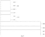
The embodiment of the present disclosure provides an array substrate shown in FIG. 11. Compared with the array substrate provided by the embodiment corresponding to FIG. 10 of the present disclosure, in order to convert more invalid light (in particular, the light emitted by the organic electroluminescence component 102 and irradiating the pixel defining layer 109, and the light incident from the outside to the interior of the display panel) into electric energy and further save energy consumption, as shown in FIG. 11, embodiment 5 of the present disclosure is provided with a groove at a position corresponding to the photoelectric conversion component 103 on one face of the pixel defining layer 109 away from the base substrate 101 (i.e. an upper surface of the pixel defining layer 109 in FIG. 11), and a side of the groove is provided with a light guiding layer 114.
The groove is used to guide light from the organic electroluminescence component 102 irradiating the light guiding layer 114 and light from the outside irradiating the bottom of the groove to the photoelectric conversion component 103.
The photoelectric conversion component 103 is not only used to convert the light of the first waveband and the second waveband emitted by the organic electroluminescence component 102, reflected by the cathode 1023, guided by the light guiding layer 114 and irradiating the base substrate 101 into electric energy, but also used to convert the light guided out through the groove and the received light from the outside into electric energy.
In the array substrate provided by the embodiment of the present disclosure, in order to better guide the light from the organic electroluminescence component 102 irradiating the light guiding layer 114 in the pixel defining layer 109 to the photoelectric conversion component 103, as shown in FIG. 11, the cross section of the groove perpendicular to the direction of the base substrate 101 may be a trapezoid structure with a wide top and a narrow bottom.
The cross section of the groove perpendicular to the direction of the base substrate 101 may further be other structures as long as the light from the organic electroluminescence component 102 irradiating the light guiding layer 114 in the pixel defining layer 109 may be guided to the photoelectric conversion component 103, which is not specifically limited here.
In the array substrate provided by the embodiment of the present disclosure, in order to achieve better reflection, the included angle α between the side of the groove and the surface of the pixel defining layer 109 away from the base substrate 101 is 10 to 80 degrees.
The depth d1 of the groove is two-thirds of the thickness d2 of the pixel defining layer 109.
The material of the light guiding layer 114 may be a metal with a reflective property.
In order to make the light reflected by the light guiding layer 114 incident on the photoelectric conversion component 103 to a large extent, as shown in FIG. 11, the positive projection of the groove on the base substrate 101 coincides with the positive projection of the photoelectric conversion component 103 on the base substrate 101.
It shall be noted that the above description only introduces the difference between the array substrate provided by the embodiment of the present disclosure and the array substrate provided by the embodiment 4 of the present disclosure. For the repetition, please refer to the above description of the embodiment 4, as no more statement is made herein.
It can be understood that the touch component 110 in the array substrate provided by the embodiment corresponding to FIG. 8 of the present disclosure may also be applied to the array substrate provided by the embodiments corresponding to FIG. 9, FIG. 10 and FIG. 11 of the present disclosure.
Moreover, according to the specific structure of the array substrate provided by the embodiments corresponding to FIG. 9, FIG. 10 and FIG. 11 of the present disclosure, it can be known that when the touch component 110 is applied to the array substrate provided by the embodiments corresponding to FIG. 9, FIG. 10 and FIG. 11 of the present disclosure, the touch component 110 is specifically located at a gap of each organic electroluminescence component 102, including a first touch electrode 1101, a second insulating layer 1102 and a second touch electrode 1103 successively located on one side of the packaging layer 104 away from the organic electroluminescence component 102. Furthermore, each film layer of the touch component 110 does not relate to the problem of multiplexing the film layer or on the same layer of the photoelectric conversion component 103.
In a specific embodiment.
Based on the same inventive concept, the embodiment of the present disclosure further provides a display panel, including an array substrate and a protection cover plate which are oppositely arranged. The array substrate is the array substrate provided by the embodiments of the present disclosure.
The display panel may be a mobile phone, a tablet computer, a TV, a display, a laptop, a digital camera, a navigator, a smart watch, a fitness wrist strap, a personal digital assistant, a self-service deposit/withdrawal machine and any other product or part with a display function.
Other essential components of the display panel that should be listed here as understood by those skilled in the art, for example, a circular polarizer arranged between the array substrate and the protection cover plate, will neither be described here, nor be regarded as a limitation to the present disclosure.
For an implementation of the display panel, please refer to the embodiment of the array substrate above, as the repetition will be omitted.
It shall be noted that in this description, relational terms such as first and second are only used to distinguish one entity or operation from another, but not necessarily to require or imply any such actual relationship or order between these entities or operations.
Obviously, those skilled in the art can make various changes and modifications to the present disclosure without departing from the spirit and scope of the present disclosure. In this way, if these changes and modifications of the present disclosure belong to the scope of the claims of the present disclosure and its equivalent technology, the present disclosure also intends to include these changes and modifications.

Claims (18)

The invention claimed is:
1. An array substrate, comprising:
a base substrate;
a plurality of organic electroluminescence components, arranged on the base substrate in an array, wherein a luminescent spectrum of each organic electroluminescence component comprises a first waveband and a second waveband, the first waveband is determined by an emission peak of the luminescent spectrum, and is configured to determine brightness and tone purity of light emitted by the organic electroluminescence component; and
at least one photoelectric conversion component, corresponding to the organic electroluminescence component, and at least configured to convert light of the second waveband emitted by the corresponding organic electroluminescence component into electric energy;
wherein the photoelectric conversion component comprises a fourth transparent electrode, a P-type semiconductor layer, an intrinsic semiconductor layer, an N-type semiconductor layer and a fifth transparent electrode arranged in a stackup manner;
wherein a material of the intrinsic semiconductor layer corresponding to the organic electroluminescence component emitting red light is amorphous silicon; a material of the intrinsic semiconductor layer corresponding to the organic electroluminescence component emitting green light is amorphous silicon doped with 5*1014 carbon particles; and a material of the intrinsic semiconductor layer corresponding to the organic electroluminescence component emitting blue light is amorphous silicon doped with 9*1013 carbon particles.
2. The array substrate according to claim 1, wherein the photoelectric conversion component is located at an edge of an area where the corresponding organic electroluminescence component is located, or located at a gap between two adjacent organic electroluminescence components.
3. The array substrate according to claim 2, wherein the photoelectric conversion component is located on a side of the organic electroluminescence component away from the base substrate; and
the array substrate further comprises:
a thermoelectric/piezoelectric conversion component, located between the photoelectric conversion component and the organic electroluminescence component, wherein the thermoelectric/piezoelectric conversion component is configured to convert thermal energy emitted by the photoelectric conversion component and pressure of the thermoelectric/piezoelectric conversion component into electric energy, and the thermoelectric/piezoelectric conversion component and the organic electroluminescence component are insulated with each other.
4. The array substrate according to claim 3, wherein positive projection of the thermoelectric/piezoelectric conversion component on the base substrate coincides with positive projection of the photoelectric conversion component on the base substrate.
5. The array substrate according to claim 4, wherein the thermoelectric/piezoelectric conversion component comprises a first transparent electrode, a thermoelectric/piezoelectric material layer and a second transparent electrode arranged successively in a stackup manner, wherein the second transparent electrode is located on a side of the thermoelectric/piezoelectric material layer facing toward the photoelectric conversion component.
6. The array substrate according to claim 5, wherein the photoelectric conversion component comprises a poly-3-hexylthiophene layer, a zinc oxide layer and a third transparent electrode successively located on a side of the second transparent electrode away from the thermoelectric/piezoelectric material layer.
7. The array substrate according to claim 1, wherein the photoelectric conversion component is located between the base substrate and a layer where the organic electroluminescence component is located, and the photoelectric conversion component is configured to convert light of the first waveband and the second waveband emitted by the organic electroluminescence component and irradiating in a direction of the base substrate.
8. The array substrate according to claim 7, further comprising:
a pixel defining layer for defining an area where each organic electroluminescence component is located;
wherein the pixel defining layer has a groove at a position corresponding to the photoelectric conversion component on a face away from the base substrate, a side of the groove comprises a light guiding layer, and the groove is configured for guiding light from the organic electroluminescence component irradiating the light guiding layer and light from outside irradiating a bottom of the groove to the photoelectric conversion component; and the photoelectric conversion component is further configured to convert the light guided out through the groove and the received light from outside into electric energy.
9. The array substrate according to claim 8, wherein a cross section of the groove perpendicular to a direction of the base substrate is a trapezoid structure with a wide top and a narrow bottom.
10. The array substrate according to claim 9, wherein an included angle between a side of the groove and a surface of the pixel defining layer away from the base substrate is 10 to 80 degrees.
11. The array substrate according to claim 8, wherein
depth of the groove is two-thirds of thickness of the pixel defining layer;
a material of the light guiding layer is a metal with a reflective property; and
positive projection of the groove on the base substrate coincides with positive projection of the photoelectric conversion component on the base substrate.
12. The array substrate according to claim 7, further comprising:
a transistor layer located between the base substrate and a layer where the organic electroluminescence component is located, wherein the photoelectric conversion component is located between the base substrate and the transistor layer.
13. The array substrate according to claim 2, wherein the photoelectric conversion component is located on a side of the organic electroluminescence component away from the base substrate, and the photoelectric conversion component is configured to convert the light of the second waveband emitted by the organic electroluminescence component and irradiating a display side into electric energy.
14. The array substrate according to claim 1, further comprising:
a first insulating layer and wiring located on a side of the fifth transparent electrode away from the N-type semiconductor layer;
wherein the first insulating layer covers side surfaces of the fourth transparent electrode, the P-type semiconductor layer, the intrinsic semiconductor layer, the N-type semiconductor layer and the fifth transparent electrode that are respectively perpendicular to the base substrate; and
the wiring is connected to the fifth transparent electrode through a via hole penetrating through the first insulating layer.
15. The array substrate according to claim 13, further comprising:
a packaging layer, arranged between the organic electroluminescence component and the photoelectric conversion component.
16. The array substrate according to claim 1, wherein the array substrate further comprises:
a touch component located at a gap of each organic electroluminescence component; and
the touch component comprises a first touch electrode, a second insulating layer and a second touch electrode arranged in a stackup manner.
17. The array substrate according to claim 16, wherein, the touch component is located on a side of the organic electroluminescence component away from the base substrate; when the photoelectric conversion component is located on the side of the organic electroluminescence component away from the base substrate, the first touch electrode and the fourth transparent electrode are arranged in a same layer, the first insulating layer is reused as the second insulating layer, and the second touch electrode and the wiring are arranged in a same layer.
18. A display panel, comprising an array substrate and a protection cover plate, wherein the array substrate comprises:
a base substrate;
a plurality of organic electroluminescence components, arranged on the base substrate in an array, wherein a luminescent spectrum of each organic electroluminescence component comprises a first waveband and a second waveband, the first waveband is determined by an emission peak of the luminescent spectrum, and is configured to determine brightness and tone purity of light emitted by the organic electroluminescence component; and
at least one photoelectric conversion component, corresponding to the organic electroluminescence component, and at least configured to convert light of the second waveband emitted by the corresponding organic electroluminescence component into electric energy;
wherein the photoelectric conversion component comprises a fourth transparent electrode, a P-type semiconductor layer, an intrinsic semiconductor layer, an N-type semiconductor layer and a fifth transparent electrode arranged in a stackup manner;
wherein a material of the intrinsic semiconductor layer corresponding to the organic electroluminescence component emitting red light is amorphous silicon; a material of the intrinsic semiconductor layer corresponding to the organic electroluminescence component emitting green light is amorphous silicon doped with 5*1014 carbon particles; and a material of the intrinsic semiconductor layer corresponding to the organic electroluminescence component emitting blue light is amorphous silicon doped with 9*1013 carbon particles.
US16/620,572 2018-09-18 2019-06-12 Array substrate and display panel Active US11222930B2 (en)

Applications Claiming Priority (3)

Application Number Priority Date Filing Date Title
CN201811086394.1 2018-09-18
CN201811086394.1A CN109346498B (en) 2018-09-18 2018-09-18 Array substrate and display panel
PCT/CN2019/090928 WO2020057185A1 (en) 2018-09-18 2019-06-12 Array substrate and display panel

Publications (2)

Publication Number Publication Date
US20210057495A1 US20210057495A1 (en) 2021-02-25
US11222930B2 true US11222930B2 (en) 2022-01-11

Family

ID=65305396

Family Applications (1)

Application Number Title Priority Date Filing Date
US16/620,572 Active US11222930B2 (en) 2018-09-18 2019-06-12 Array substrate and display panel

Country Status (3)

Country Link
US (1) US11222930B2 (en)
CN (1) CN109346498B (en)
WO (1) WO2020057185A1 (en)

Cited By (1)

* Cited by examiner, † Cited by third party
Publication number Priority date Publication date Assignee Title
US11502138B2 (en) * 2019-06-27 2022-11-15 Chengdu Boe Optoelectronics Technology Co., Ltd. Electronic substrate, manufacturing method thereof, and display panel

Families Citing this family (3)

* Cited by examiner, † Cited by third party
Publication number Priority date Publication date Assignee Title
CN109346498B (en) * 2018-09-18 2020-06-16 京东方科技集团股份有限公司 Array substrate and display panel
CN110767726B (en) * 2019-10-29 2022-07-15 昆山国显光电有限公司 Method for improving color cast, display panel and display device
CN111524937B (en) * 2020-04-23 2021-08-24 深圳市华星光电半导体显示技术有限公司 OLED display panel and display device

Citations (16)

* Cited by examiner, † Cited by third party
Publication number Priority date Publication date Assignee Title
US20130285046A1 (en) * 2012-04-25 2013-10-31 Semiconductor Energy Laboratory Co., Ltd. Semiconductor device and method of manufacturing the same
CN104201187A (en) 2014-08-18 2014-12-10 京东方科技集团股份有限公司 Organic light emitting diode (OLED) display device
CN104752462A (en) 2013-12-27 2015-07-01 昆山国显光电有限公司 Organic light emitting diode (OLED) display with touch panel
US20150279884A1 (en) * 2014-03-28 2015-10-01 Semiconductor Energy Laboratory Co., Ltd. Imaging device
US20150364527A1 (en) * 2014-06-11 2015-12-17 Samsung Display Co., Ltd. Organic light emitting diode display including sensors
US20160155782A1 (en) * 2014-12-01 2016-06-02 Japan Display Inc. Display device
US20170357641A1 (en) * 2016-06-10 2017-12-14 Semiconductor Energy Laboratory Co., Ltd. Information terminal
CN107506728A (en) * 2017-08-23 2017-12-22 京东方科技集团股份有限公司 Photosensitive unit, photosensitive module and photosensitive device
US20180060641A1 (en) * 2016-08-23 2018-03-01 Samsung Display Co., Ltd. Method and apparatus to detect three-dimensional pattern information of a touch object
US20180074614A1 (en) * 2016-09-13 2018-03-15 Japan Display Inc. Display device and electric device
CN109346498A (en) 2018-09-18 2019-02-15 京东方科技集团股份有限公司 A kind of array substrate and display panel
US20190384428A1 (en) * 2016-07-21 2019-12-19 Dongwoo Fine-Chem Co., Ltd. Film touch sensor
US20200242324A1 (en) * 2018-07-20 2020-07-30 Boe Technology Group Co., Ltd. Array substrate, method of manufacturing array substrate, and display apparatus
US20200350374A1 (en) * 2018-08-01 2020-11-05 Boe Technology Group Co., Ltd. Display panel, manufacturing method thereof, and display device
US20210124441A1 (en) * 2019-10-23 2021-04-29 Boe Technology Group Co., Ltd. Display substrate, display device and detection method by using display device
US20210134896A1 (en) * 2019-01-30 2021-05-06 Boe Technology Group Co., Ltd. Display panel and display apparatus

Family Cites Families (1)

* Cited by examiner, † Cited by third party
Publication number Priority date Publication date Assignee Title
CN107589576B (en) * 2017-09-30 2020-11-06 武汉华星光电技术有限公司 Array substrate, manufacturing method thereof and touch display panel

Patent Citations (17)

* Cited by examiner, † Cited by third party
Publication number Priority date Publication date Assignee Title
US20130285046A1 (en) * 2012-04-25 2013-10-31 Semiconductor Energy Laboratory Co., Ltd. Semiconductor device and method of manufacturing the same
CN104752462A (en) 2013-12-27 2015-07-01 昆山国显光电有限公司 Organic light emitting diode (OLED) display with touch panel
US20150279884A1 (en) * 2014-03-28 2015-10-01 Semiconductor Energy Laboratory Co., Ltd. Imaging device
US20150364527A1 (en) * 2014-06-11 2015-12-17 Samsung Display Co., Ltd. Organic light emitting diode display including sensors
CN104201187A (en) 2014-08-18 2014-12-10 京东方科技集团股份有限公司 Organic light emitting diode (OLED) display device
US20160293100A1 (en) 2014-08-18 2016-10-06 Boe Technology Group Co., Ltd. Organic light-emitting diode display apparatus, display device, and method for testing the organic light-emitting diode display apparatus
US20160155782A1 (en) * 2014-12-01 2016-06-02 Japan Display Inc. Display device
US20170357641A1 (en) * 2016-06-10 2017-12-14 Semiconductor Energy Laboratory Co., Ltd. Information terminal
US20190384428A1 (en) * 2016-07-21 2019-12-19 Dongwoo Fine-Chem Co., Ltd. Film touch sensor
US20180060641A1 (en) * 2016-08-23 2018-03-01 Samsung Display Co., Ltd. Method and apparatus to detect three-dimensional pattern information of a touch object
US20180074614A1 (en) * 2016-09-13 2018-03-15 Japan Display Inc. Display device and electric device
CN107506728A (en) * 2017-08-23 2017-12-22 京东方科技集团股份有限公司 Photosensitive unit, photosensitive module and photosensitive device
US20200242324A1 (en) * 2018-07-20 2020-07-30 Boe Technology Group Co., Ltd. Array substrate, method of manufacturing array substrate, and display apparatus
US20200350374A1 (en) * 2018-08-01 2020-11-05 Boe Technology Group Co., Ltd. Display panel, manufacturing method thereof, and display device
CN109346498A (en) 2018-09-18 2019-02-15 京东方科技集团股份有限公司 A kind of array substrate and display panel
US20210134896A1 (en) * 2019-01-30 2021-05-06 Boe Technology Group Co., Ltd. Display panel and display apparatus
US20210124441A1 (en) * 2019-10-23 2021-04-29 Boe Technology Group Co., Ltd. Display substrate, display device and detection method by using display device

Non-Patent Citations (1)

* Cited by examiner, † Cited by third party
Title
First Chinese Office Action issued in Chinese Patent Application No. 201811086394.1 dated Dec. 20, 2019.

Cited By (1)

* Cited by examiner, † Cited by third party
Publication number Priority date Publication date Assignee Title
US11502138B2 (en) * 2019-06-27 2022-11-15 Chengdu Boe Optoelectronics Technology Co., Ltd. Electronic substrate, manufacturing method thereof, and display panel

Also Published As

Publication number Publication date
CN109346498A (en) 2019-02-15
US20210057495A1 (en) 2021-02-25
WO2020057185A1 (en) 2020-03-26
CN109346498B (en) 2020-06-16

Similar Documents

Publication Publication Date Title
US11222930B2 (en) Array substrate and display panel
US10535719B2 (en) Color film substrate for WOLED display and WOLED display
US9786721B1 (en) OLED display panel
US9960212B2 (en) Organic light emitting diode display panel
JP2016195136A (en) Light emitting device
US8476622B2 (en) Active matrix organic light emitting diode
US20090051275A1 (en) Light emitting device
KR20100024710A (en) Organic light emitting diode display
KR20110065852A (en) Organic light emitting display apparatus and method of manufacturing thereof
WO2016150030A1 (en) Oled substrate and manufacturing method therefor, oled display panel, and electronic device
US10741731B2 (en) Multi-emission quantum dot and quantum dot film, LED package, emitting diode and display device including the same
US9660219B2 (en) Methods of manufacturing display devices
WO2020056865A1 (en) Display panel and display device
KR20140087813A (en) Organic Light Emitting Diode Display Device and Method for Manufacturing The Same
KR20120044655A (en) Organic light emitting diode display
CN107634084B (en) Top-emitting white light OLED display device
US11309513B2 (en) Anode, light emitting device, display substrate and method of manufacturing the same, and display device
US20210336236A1 (en) Display panel and manufacturing method thereof
KR101068395B1 (en) top emission type Organic Electro luminescence Device and fabrication method thereof
US10367038B2 (en) Organic light-emitting diode display device and manufacturing method thereof, and organic light-emitting diode display
US11189674B2 (en) Anode structure, method of forming the same and organic light emitting diode display device including the same
US11950450B2 (en) Display substrate and method of manufacturing the same and electronic device
WO2022227452A1 (en) Top-emission display panel and display apparatus
WO2019153401A1 (en) Oled display panel
US9324770B2 (en) Organic light emitting display devices and methods of manufacturing organic light emitting display devices

Legal Events

Date Code Title Description
AS Assignment

Owner name: BOE TECHNOLOGY GROUP CO., LTD., CHINA

Free format text: ASSIGNMENT OF ASSIGNORS INTEREST;ASSIGNORS:YUAN, GUANGCAI;GUO, KANG;GU, XIN;AND OTHERS;REEL/FRAME:051214/0810

Effective date: 20191203

FEPP Fee payment procedure

Free format text: ENTITY STATUS SET TO UNDISCOUNTED (ORIGINAL EVENT CODE: BIG.); ENTITY STATUS OF PATENT OWNER: LARGE ENTITY

STPP Information on status: patent application and granting procedure in general

Free format text: DOCKETED NEW CASE - READY FOR EXAMINATION

STPP Information on status: patent application and granting procedure in general

Free format text: NON FINAL ACTION MAILED

STPP Information on status: patent application and granting procedure in general

Free format text: RESPONSE TO NON-FINAL OFFICE ACTION ENTERED AND FORWARDED TO EXAMINER

STPP Information on status: patent application and granting procedure in general

Free format text: NOTICE OF ALLOWANCE MAILED -- APPLICATION RECEIVED IN OFFICE OF PUBLICATIONS

STPP Information on status: patent application and granting procedure in general

Free format text: PUBLICATIONS -- ISSUE FEE PAYMENT RECEIVED

STPP Information on status: patent application and granting procedure in general

Free format text: PUBLICATIONS -- ISSUE FEE PAYMENT VERIFIED

STCF Information on status: patent grant

Free format text: PATENTED CASE