US11221794B2 - Memory array element sparing - Google Patents
Memory array element sparing Download PDFInfo
- Publication number
- US11221794B2 US11221794B2 US16/280,577 US201916280577A US11221794B2 US 11221794 B2 US11221794 B2 US 11221794B2 US 201916280577 A US201916280577 A US 201916280577A US 11221794 B2 US11221794 B2 US 11221794B2
- Authority
- US
- United States
- Prior art keywords
- column
- memory array
- array element
- columns
- defective
- Prior art date
- Legal status (The legal status is an assumption and is not a legal conclusion. Google has not performed a legal analysis and makes no representation as to the accuracy of the status listed.)
- Active
Links
Images


Classifications
-
- G—PHYSICS
- G06—COMPUTING; CALCULATING OR COUNTING
- G06F—ELECTRIC DIGITAL DATA PROCESSING
- G06F3/00—Input arrangements for transferring data to be processed into a form capable of being handled by the computer; Output arrangements for transferring data from processing unit to output unit, e.g. interface arrangements
- G06F3/06—Digital input from, or digital output to, record carriers, e.g. RAID, emulated record carriers or networked record carriers
- G06F3/0601—Interfaces specially adapted for storage systems
- G06F3/0628—Interfaces specially adapted for storage systems making use of a particular technique
- G06F3/0655—Vertical data movement, i.e. input-output transfer; data movement between one or more hosts and one or more storage devices
- G06F3/0659—Command handling arrangements, e.g. command buffers, queues, command scheduling
-
- G—PHYSICS
- G06—COMPUTING; CALCULATING OR COUNTING
- G06F—ELECTRIC DIGITAL DATA PROCESSING
- G06F12/00—Accessing, addressing or allocating within memory systems or architectures
- G06F12/02—Addressing or allocation; Relocation
- G06F12/08—Addressing or allocation; Relocation in hierarchically structured memory systems, e.g. virtual memory systems
- G06F12/0802—Addressing of a memory level in which the access to the desired data or data block requires associative addressing means, e.g. caches
- G06F12/0806—Multiuser, multiprocessor or multiprocessing cache systems
- G06F12/0811—Multiuser, multiprocessor or multiprocessing cache systems with multilevel cache hierarchies
-
- G—PHYSICS
- G06—COMPUTING; CALCULATING OR COUNTING
- G06F—ELECTRIC DIGITAL DATA PROCESSING
- G06F11/00—Error detection; Error correction; Monitoring
- G06F11/07—Responding to the occurrence of a fault, e.g. fault tolerance
- G06F11/0703—Error or fault processing not based on redundancy, i.e. by taking additional measures to deal with the error or fault not making use of redundancy in operation, in hardware, or in data representation
- G06F11/0751—Error or fault detection not based on redundancy
-
- G—PHYSICS
- G06—COMPUTING; CALCULATING OR COUNTING
- G06F—ELECTRIC DIGITAL DATA PROCESSING
- G06F11/00—Error detection; Error correction; Monitoring
- G06F11/07—Responding to the occurrence of a fault, e.g. fault tolerance
- G06F11/0703—Error or fault processing not based on redundancy, i.e. by taking additional measures to deal with the error or fault not making use of redundancy in operation, in hardware, or in data representation
- G06F11/0793—Remedial or corrective actions
-
- G—PHYSICS
- G06—COMPUTING; CALCULATING OR COUNTING
- G06F—ELECTRIC DIGITAL DATA PROCESSING
- G06F11/00—Error detection; Error correction; Monitoring
- G06F11/07—Responding to the occurrence of a fault, e.g. fault tolerance
- G06F11/16—Error detection or correction of the data by redundancy in hardware
- G06F11/1666—Error detection or correction of the data by redundancy in hardware where the redundant component is memory or memory area
-
- G—PHYSICS
- G06—COMPUTING; CALCULATING OR COUNTING
- G06F—ELECTRIC DIGITAL DATA PROCESSING
- G06F12/00—Accessing, addressing or allocating within memory systems or architectures
- G06F12/02—Addressing or allocation; Relocation
- G06F12/08—Addressing or allocation; Relocation in hierarchically structured memory systems, e.g. virtual memory systems
- G06F12/0802—Addressing of a memory level in which the access to the desired data or data block requires associative addressing means, e.g. caches
- G06F12/0806—Multiuser, multiprocessor or multiprocessing cache systems
- G06F12/084—Multiuser, multiprocessor or multiprocessing cache systems with a shared cache
-
- G—PHYSICS
- G06—COMPUTING; CALCULATING OR COUNTING
- G06F—ELECTRIC DIGITAL DATA PROCESSING
- G06F12/00—Accessing, addressing or allocating within memory systems or architectures
- G06F12/02—Addressing or allocation; Relocation
- G06F12/08—Addressing or allocation; Relocation in hierarchically structured memory systems, e.g. virtual memory systems
- G06F12/0802—Addressing of a memory level in which the access to the desired data or data block requires associative addressing means, e.g. caches
- G06F12/0893—Caches characterised by their organisation or structure
- G06F12/0895—Caches characterised by their organisation or structure of parts of caches, e.g. directory or tag array
-
- G—PHYSICS
- G06—COMPUTING; CALCULATING OR COUNTING
- G06F—ELECTRIC DIGITAL DATA PROCESSING
- G06F3/00—Input arrangements for transferring data to be processed into a form capable of being handled by the computer; Output arrangements for transferring data from processing unit to output unit, e.g. interface arrangements
- G06F3/06—Digital input from, or digital output to, record carriers, e.g. RAID, emulated record carriers or networked record carriers
- G06F3/0601—Interfaces specially adapted for storage systems
- G06F3/0602—Interfaces specially adapted for storage systems specifically adapted to achieve a particular effect
- G06F3/0614—Improving the reliability of storage systems
- G06F3/0619—Improving the reliability of storage systems in relation to data integrity, e.g. data losses, bit errors
-
- G—PHYSICS
- G06—COMPUTING; CALCULATING OR COUNTING
- G06F—ELECTRIC DIGITAL DATA PROCESSING
- G06F3/00—Input arrangements for transferring data to be processed into a form capable of being handled by the computer; Output arrangements for transferring data from processing unit to output unit, e.g. interface arrangements
- G06F3/06—Digital input from, or digital output to, record carriers, e.g. RAID, emulated record carriers or networked record carriers
- G06F3/0601—Interfaces specially adapted for storage systems
- G06F3/0668—Interfaces specially adapted for storage systems adopting a particular infrastructure
- G06F3/0671—In-line storage system
- G06F3/0683—Plurality of storage devices
-
- G—PHYSICS
- G11—INFORMATION STORAGE
- G11C—STATIC STORES
- G11C29/00—Checking stores for correct operation ; Subsequent repair; Testing stores during standby or offline operation
- G11C29/70—Masking faults in memories by using spares or by reconfiguring
- G11C29/76—Masking faults in memories by using spares or by reconfiguring using address translation or modifications
-
- G—PHYSICS
- G11—INFORMATION STORAGE
- G11C—STATIC STORES
- G11C29/00—Checking stores for correct operation ; Subsequent repair; Testing stores during standby or offline operation
- G11C29/70—Masking faults in memories by using spares or by reconfiguring
- G11C29/78—Masking faults in memories by using spares or by reconfiguring using programmable devices
- G11C29/783—Masking faults in memories by using spares or by reconfiguring using programmable devices with refresh of replacement cells, e.g. in DRAMs
-
- G—PHYSICS
- G06—COMPUTING; CALCULATING OR COUNTING
- G06F—ELECTRIC DIGITAL DATA PROCESSING
- G06F2212/00—Indexing scheme relating to accessing, addressing or allocation within memory systems or architectures
- G06F2212/10—Providing a specific technical effect
- G06F2212/1032—Reliability improvement, data loss prevention, degraded operation etc
-
- G—PHYSICS
- G06—COMPUTING; CALCULATING OR COUNTING
- G06F—ELECTRIC DIGITAL DATA PROCESSING
- G06F2212/00—Indexing scheme relating to accessing, addressing or allocation within memory systems or architectures
- G06F2212/60—Details of cache memory
- G06F2212/608—Details relating to cache mapping
Definitions
- the present invention generally relates to data processing, and more specifically, to providing access to a spare eDRAM.
- SMP symmetric multiprocessing
- L4 caches can include a plurality of memory elements, such as a bank of embedded dynamic random-access memories (eDRAMs), which may be organized as an array of logical columns and rows. If a particular memory element in an array is defective, it is generally necessary to repair the array in some manner or discontinue use of the array, which can result in a loss of memory capacity.
- eDRAMs embedded dynamic random-access memories
- Embodiments of the present invention are directed to a computer-implemented method for providing access to a spare memory array element.
- a non-limiting example of the computer-implemented method includes storing a row number and a column number that are associated with a defective memory array element of a plurality of memory array elements.
- the plurality of memory array elements are logically arranged in a plurality of rows and a plurality of columns.
- the method also includes receiving a command to access a cache line.
- the cache line corresponds to a selected row of memory array elements of the plurality of memory array elements.
- the method Responsive to determining that the selected row matches the row number that is associated with the defective memory array element, the method also includes activating one or more column shifters to prevent access to the defective memory array element and provide access to a spare memory array element when accessing the cache line.
- the activation of the one or more column shifters is based on the column number that is associated with the defective memory array element.
- Embodiments of the present invention are directed to a system for providing access to a spare memory array element.
- the system includes a memory having computer readable computer instructions, and a processor for executing the computer readable instructions.
- the computer readable instructions include instructions for storing a row number and a column number that are associated with a defective memory array element of a plurality of memory array elements.
- the plurality of memory array elements are logically arranged in a plurality of rows and a plurality of columns.
- the computer readable instructions also include instructions for receiving a command to access a cache line.
- the cache line corresponds to a selected row of memory array elements of the plurality of memory array elements.
- the computer readable instructions Responsive to determining that the selected row matches the row number that is associated with the defective memory array element, the computer readable instructions also include instructions for activating one or more column shifters to prevent access to the defective memory array element and provide access to a spare memory array element when accessing the cache line. The activation of the one or more column shifters is based on the column number that is associated with the defective memory array element.
- Embodiments of the invention are directed to a computer program product for providing access to a spare memory array element, the computer program product having a computer readable storage medium having program instructions embodied therewith.
- the computer readable storage medium is not a transitory signal per se.
- the program instructions are executable by a processor to cause the processor to perform a method.
- a non-limiting example of the method includes storing a row number and a column number that are associated with a defective memory array element of a plurality of memory array elements.
- the plurality of memory array elements are logically arranged in a plurality of rows and a plurality of columns.
- the method also includes receiving a command to access a cache line.
- the cache line corresponds to a selected row of memory array elements of the plurality of memory array elements.
- the method Responsive to determining that the selected row matches the row number that is associated with the defective memory array element, the method also includes activating one or more column shifters to prevent access to the defective memory array element and provide access to a spare memory array element when accessing the cache line.
- the activation of the one or more column shifters is based on the column number that is associated with the defective memory array element.
- FIG. 1 depicts a block diagram of a distributed symmetric multiprocessing (SMP) system in accordance with one or more embodiments of the invention
- FIG. 2 depicts a block diagram of a drawer in a distributed symmetric multiprocessing (SMP) system in accordance with one or more embodiments of the invention
- FIG. 3 depicts a block diagram of an exemplary symmetric multiprocessor (SMP) computer according to one or more embodiments of the invention
- FIG. 4A depicts an example of a cache bank including store data paths for a plurality of eDRAMs and a spare eDRAM according to one or more embodiments of the invention
- FIG. 4B depicts an example of cache bank including fetch data paths for a plurality of eDRAMs and a spare eDRAM according to one or more embodiments of the invention
- FIG. 5A depicts example column shifters for cache eDRAM store data according to one or more embodiments of the invention
- FIG. 5B depicts example column shifters for cache eDRAM fetch data according to one or more embodiments of the invention.
- FIG. 6 depicts a flow diagram of a method for providing access to a spare eDRAM according to one or more embodiments of the invention.
- compositions comprising, “comprising,” “includes,” “including,” “has,” “having,” “contains” or “containing,” or any other variation thereof, are intended to cover a non-exclusive inclusion.
- a composition, a mixture, process, method, article, or apparatus that comprises a list of elements is not necessarily limited to only those elements but can include other elements not expressly listed or inherent to such composition, mixture, process, method, article, or apparatus.
- exemplary is used herein to mean “serving as an example, instance or illustration.” Any embodiment or design described herein as “exemplary” is not necessarily to be construed as preferred or advantageous over other embodiments or designs.
- the terms “at least one” and “one or more” may be understood to include any integer number greater than or equal to one, i.e. one, two, three, four, etc.
- the terms “a plurality” may be understood to include any integer number greater than or equal to two, i.e. two, three, four, five, etc.
- connection may include both an indirect “connection” and a direct “connection.”
- redundancy in regular structures improves the manufacturing yield of computer chips when defective elements can be selectively replaced by available redundant elements.
- redundancy of entire array instances can further improve yield as compared to redundancy only of elements within each array instance.
- the benefits of adding redundant (i.e., spare) array instances typically comes at a high price in terms of limited chip resources.
- Embodiments of the present invention address this problem by incorporating a plurality of column shifters into an array that allow for the use of a single spare array element to remedy a defective array element. This solution requires minimal extra wiring and switching resources, thereby dramatically improving yield with no loss in capacity or performance. Further, in addition to utilizing spares to remedy defective arrays during system testing, these spares can also be activated under firmware control to effectively repair defects that develop after the system has been shipped.
- eDRAM dynamic random-access memory
- SRAM static random-access memory
- eSRAM embedded static random-access memory
- the term “memory array element” can alternatively refer to an eDRAM, a DRAM, an SRAM or an eSRAM.
- a hierarchy of caches is used to buffer memory cache lines in order to reduce the access time overhead of data in memory.
- Highly distributed, large symmetric multiprocessing (SMP) systems can share high-level cache (e.g., IA cache).
- Prior SMP systems required tradeoffs to be made between the amount of available L4 cache and the level of connectivity between processors to accommodate cost and packaging constraints.
- Existing SMP systems can include multiple drawers, where each drawer contains two independent and separate nodes. These nodes in turn each contain multiple central processing (CP) chips (e.g., integrated circuits) connected together with a dedicated shared cache (SC) chip.
- CP chip is a chip multiprocessor (CMP) with a private L1 and L2 cache per processor and one L3 cache shared by all the processors on the chip.
- the SC chip includes an L4 cache and system interconnect logic.
- FIG. 1 depicts a distributed symmetric multiprocessing (SMP) system 100 (hereafter “system 100 ”) in accordance with one or more embodiments.
- system 100 can include 4 processing units or “drawers.”
- system 100 can include 5 processing units or drawers.
- Each drawer of system 100 can connect to the other drawers of the system 100 .
- drawer 102 (described in greater detail with respect to FIG. 2 ) connects to drawer 104 , drawer 106 , and drawer 108 via a shared cache (SC) chip (sometimes referred to as an integrated circuit (IC)) 110 .
- SC shared cache
- Drawers 104 , 106 , and 108 each have a respective SC chip (e.g., SC chip 112 , SC chip 114 , SC chip 116 ).
- Bus lines 118 connect drawers 102 , 104 , 106 , and 108 . Intra-drawer coherency communication may be performed using pass-through and a combination of these bus-lines, 118 .
- cache lines that are owned or shared by processors of an entity at a level of coherency are candidates to be handled at the level of coherency.
- a processor of the entity requests ownership or sharing of a line that is already owned by a processor of the same entity (e.g., CP Chip or drawer)
- the entity need not access other entities to handle the request coherently.
- a request for example, by a processor of a CP chip within a CP cluster, for sharing of a cache line is examined by memory controller function to determine if the line is owned or shared by a processor of CP cluster. If it is already owned or shared, the memory controller handles the request within the CP cluster without accessing any other CP clusters.
- the memory controller of the initial CP Cluster performs a cache coherency operation with the other CP chips on the other CP clusters connected to that SC chip or on the other drawers via the SC chips on those drawers.
- FIG. 2 depicts drawer 102 in greater detail, according to one or more embodiments. Although FIG. 2 depicts only drawer 102 , it should be appreciated that a similar configuration is contemplated for drawers 104 , 106 , and 108 , and/or other drawers in system 100 .
- drawer 102 includes two CP clusters (e.g., CP cluster 121 and CP cluster 123 ). Each CP cluster contains individual CP chips.
- CP cluster 121 contains CP chips 122 a , 122 b , and 122 c ; and CP cluster 123 contains CP chips 124 a , 124 b , and 124 c .
- Each of the individual CP chips (e.g., CP chips 122 a , 122 b , 122 c , 124 a , 124 b , 124 c ) has multiple processing cores (e.g., 2 processing cores, 8 processing cores, 10 processing cores, etc.) and each processing core has its own private L1 and L2 cache.
- the processing cores within each individual CP chip share an L3 cache at the CP level.
- the CP 122 a includes multiple processing cores that each has its own L1/L2 cache and the multiple processing cores within the CP 121 share an L3 cache.
- Each respective CP chip may be connected to system memory (e.g., system memory 212 , system memory 214 , system memory 216 , and system memory 218 ).
- CP chip 121 is operatively connected with each of the other clusters (e.g., 123 ) via bus lines 130 through the SC chip 110 .
- a CP cluster may include any number of CP chips, although embodiments are described as having only three.
- the SC chip 110 includes interconnects for communication with each CP chip (e.g., CP chips 122 a , 122 b , 122 c , 124 a , 124 b , 124 c ) in both clusters 121 , 123 on the drawer 102 and for communication with other SC chips on other drawers (e.g., the SC 112 of the drawer 104 , the SC 114 of the drawer 106 , the SC 116 of the drawer 108 , etc.).
- the SC chip 110 includes an L4 cache 220 and directory that includes the L4 cache and a directory of the state bits.
- FIG. 3 depicts a block diagram of an exemplary symmetric multiprocessor (SMP) computer according to one or more embodiments of the present invention.
- the system 300 includes several CP clusters 330 a - 330 N (where N is any whole number greater than 2) which may be directly connected or connected through other SC chips. As described in FIG. 2 , each CP cluster includes three CP chips.
- CP chip 122 a is depicted in greater detail in FIG. 3 .
- CP chip 122 a includes processors 302 a - 302 N (where N is any whole number greater than 2).
- Each processor has one or more cores 304 , an L1 cache 306 , and an L2 cache 308 .
- Each processor within the CP chip 122 a is communicatively coupled to a memory controller 312 on a shared cache level 310 .
- the memory controller 312 can access the L3 cache 314 .
- each of the processors 302 a - 302 N share the L3 cache on the CP chip 122 a .
- the memory controller 312 with the L3 cache implements a shared cache level 310 across a CP cluster in the system 300 .
- the main memory 320 can include a random access store of program data and program instructions for data processing on the system 300 .
- Main memory 320 is characterized by memory latency, the time required for a memory access, a read or write to or from main memory.
- the L1 cache 306 and L2 cache 308 along with the L3 cache 314 are specialized segments of memory used by the processors 302 a - 302 N to reduce memory access latency.
- Each cache, including L4 cache 220 is smaller and faster than main memory 320 , and each cache stores copies of data from frequently used main memory locations.
- a processor needs to read from or write to a location in memory, it first checks whether a copy of that data, a “cache line,” is in a cache.
- the SC chip 110 will initiate requests to the SC Chips on the other drawers 340 a . . . 340 N. If the cache line is not contained in any of the caches on any of the drawers, the memory controller 312 (on the drawer whose memory contains the line) will request the line from memory. If the memory containing the cache line is on any of the drawers 340 a . . .
- the line is fetched from memory there, sent to the SC chip on that drawer, which forwards it to the SC chip on the drawer where the processor 302 a fetch request originated. If the memory containing the cache line is on the same drawer where the processor 302 a fetch request originated, the memory controller 312 retrieves the line from memory. In all scenarios where a line is fetched from memory, either locally 320 or from memory on a remote drawer 340 a . . . 340 N, the line is delivered to the requesting processor 302 a and also installed in all levels of cache, L1, L2, L3, and L4 on the requesting drawer.
- an L4 cache 220 may include, for example, 960 MB of cache data capacity that includes 3,776 2 Mb eDRAM macros per SC chip 110 , organized as a 60-way set associative cache with 65,536 (64k) sets or congruence classes and 256 bytes per cache line.
- each way of an n-way cache set may be referred to as a compartment.
- a 60-way set associative cache can be said to have 60 compartments per set or congruence class.
- an “eDRAM macro” may refer to a standardized eDRAM array instance that can be reused throughout the system.
- each SC chip 110 may be divided into four quadrants, with 944 eDRAM macros per quadrant.
- each quadrant may include four cache banks, and each cache bank may include 236 eDRAM macros.
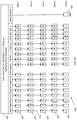
- FIG. 4A shows an example cache bank 400 having a plurality of 235 eDRAMs 402 and one spare eDRAM 404 , for a total of 236 eDRAMs in the cache bank 400 .
- a cache bank 400 of an SC quadrant may include a plurality of eDRAMs 402 that are logically arranged into a number of columns and a number of rows.
- logical arrangement of eDRAMs 402 into a number of rows and columns mean that the eDRAMs 402 are not necessarily physically arranged into rows and columns within the L4 cache 220 , but rather are connected and/or indexed in a manner that is representative of rows and columns.
- the plurality of eDRAMs 402 may be logically arranged into 5 rows and 47 columns.
- each row of eDRAMs 402 may store a plurality of quad words using a number of eDRAMs of the row (e.g., data quad words may be stored by the first 43 columns of eDRAMs 402 of each row).
- Each data quad word may be 16 bytes of data that is made up of 43 3-bit symbols (e.g., 128 bits of data and 1 unused bit).
- a 3-bit symbol may be read out of each eDRAM 402 of a row to form a given data quad word.
- fetching a data quad word an entire row of eDRAMs 402 may be accessed, with a number of the eDRAMs 402 of the row (e.g., the last 4 eDRAMs) containing data that is used for error checking.
- a cache line may be made up of 16 data quad words.
- the system may access a particular row of eDRAMs and read out 16 data quad words over 16 successive cycles.
- each row of eDRAMs 402 may supply 12-way set associativity for a total of 60-way set associativity across 5 rows in a bank 400 .
- each addressable internal row of an eDRAM macro hereafter referred to as an eDRAM internal row, may contain a portion of one congruence class, such that an eDRAM internal row of 47 eDRAMs 402 , may contain 12 compartments from one congruence class plus ECC protection, or put another way, each internal eDRAM row from a combined group or row of 47 eDRAMs 402 contains one 12-way set associative congruence class with ECC protection included.
- each SC chip 110 may include 64,536 (64k) congruence classes (i.e., 4,096 per bank*4 banks per quadrant*4 quadrants per chip) with each congruence class having 60 compartments or 60-way set associativity.
- each column of eDRAMs 402 may be connected to staging and storage circuitry 406 that can be used to stage data (i.e., temporarily store data in latches or registers as necessary based on computer cycle-based physical limitations to data transmission), generate ECC protection symbols, and store data and ECC in the plurality of eDRAMs 402 as well as the spare eDRAM 404 in accordance with embodiments of the invention described herein.
- store data can be multi-dropped to each row in a cache bank 400 , where selective write controls may be used to store data in the desired internal eDRAM row of the desired row (A, B, C, D, or E) of eDRAMs 402 , where each row of eDRAMs 402 contains 12 of the total 60 associativity classes or compartments per bank 400 .
- FIG. 4A is a common address bus connected to every eDRAM 402 in each cache bank 400 , where this address bus causes one of the 4096 internal eDRAM rows to be selected for access in each row of eDRAM's 402 . As shown in FIG.
- each column of eDRAMs 402 , as well as the spare eDRAM 404 may be connected to fetch and error correction circuitry 408 that can be used to fetch data from the plurality of eDRAMs 402 , as well as the spare eDRAM 404 , and perform error correction functionalities with respect to the data.
- cascading multiplexers 410 disposed between each row of eDRAMs may be used to selectively deliver fetch data from a desired internal eDRAM row of the desired row (A, B, C, D or E) of eDRAMs 402 . For example, as shown in FIG.
- a first multiplexer 410 may receive the outputs of eDRAMs 402 in rows A and B as inputs
- a second multiplexer 410 may receive the output of the first multiplexer 410 and the output of an eDRAM 402 in row C as inputs
- a third multiplexer 410 may receive the output of the second multiplexer and the output of an eDRAM 402 in row D as inputs
- a fourth multiplexer 410 may receive the output of the third multiplexer 410 and an eDRAM 402 in row E as inputs and provide the output of the fourth multiplexer 410 as an input to the fetch and error correction circuitry 408 . Not shown in FIG.
- 4B is a common address bus connected to every eDRAM 402 in each cache bank 400 , where this address bus causes one of the 4096 internal eDRAM rows to be selected for access in each row of eDRAM's 402 .
- the outputs of the fourth multiplexer 410 in each column of eDRAMs 402 may converge at the fetch and error correction circuitry 408 , allowing an error-checked and corrected data quad word to be read out of the plurality of eDRAMs 402 as a plurality of 3-bit symbols.
- eDRAMs 402 of each column of eDRAMs 402 are connected by a common fetch bus 413 , during a fetching operation, only one row of a column is accessed.
- the row of an eDRAM 402 accessed pursuant to the execution of an instruction can impact whether or not eDRAM sparing is utilized during the execution of the instruction.
- the system can selectively activate one or more column shifters 502 , 504 to essentially displace the defective eDRAM 402 with the spare eDRAM 404 to allow uninterrupted operation of the cache bank 400 .
- a single spare eDRAM 404 can serve to repair a defective eDRAM 402 without requiring the need of additional rows or columns of spare eDRAMs, which would require significantly more space and are likely to be underutilized if, for example, only a single eDRAM of an entire replacement row of eDRAMs is used to repair a single defective eDRAM (i.e., the unused eDRAMs of the replacement row are wasted).
- the system may not activate any column shifters 502 , 504 , but may instead allow the fetch/store operation to execute as it would under normal conditions.
- FIGS. 5A and 5B show example column shifters 502 , 504 in accordance with embodiments of the invention that can be used for data storage and data fetching operations, respectively, to repair the cache bank 400 in a case where an eDRAM 402 of the plurality of eDRAMs 402 is determined to be defective.
- store column shifters 502 for use in association with storage operations may be integrated into the staging and storage circuitry 406 in a manner such that the column shifters can receive data or symbol inputs (e.g., retrieved from a processor, from memory, from an input/output device, etc.) at the staging and storage circuitry 406 . As shown in FIG.
- each store column shifter 502 can have a first output path to a first column and a second output path to a second column that is adjacent to the first column.
- the number of store column shifters 502 may be one less than the number of columns of eDRAMs 402 .
- a store column shifter 502 may be a multiplexer that receives two inputs and selects one of the two inputs as an output based on a control signal received from a controller.
- Each store column shifter 502 can be selectively controlled by controller(s) or control logic included in each cache bank 400 to activate or deactivate a shifting function provided by the store column shifter 502 .
- controllers or control logic may be included in the L4 cache 220 .
- one of the inputs received by a store column shifter 502 can be from the same logical column as the output of the column shifter 502 , and the second input can be from an adjacent column.
- a first store column shifter 502 having an output at Column 1 may receive inputs from Symbol 0 and Symbol 1
- a second column shifter 502 having an output at Column 2 may receive inputs from Symbol 1 and Symbol 2
- the default state of a store column shifter 502 is inactive, and when in an inactive state the store column shifter 502 will not provide a shifting function, but will instead allow an input symbol to pass through to the corresponding column for storage in an eDRAM 402 of the column.
- the store column shifter 502 having an output to Column 1 when the store column shifter 502 having an output to Column 1 is in an inactive state, it will select Symbol 1 as the input to pass along to the output (i.e., selecting the R path). However, when a store column shifter 502 is switched to an active state, the store column shifter 502 will select the alternate input to pass through as an output. For example, when the store column shifter 502 having an output to Column 1 is in an active state, it will select the input received from Symbol 0 (i.e., selecting the L path) to pass along as the output to Column 1 . In this way, the store column shifter can shift an input symbol that is logically input at a first column and shift it to be stored in an eDRAM of a logically adjacent second column.
- the final store column shifter 502 of a row i.e., the column shifter 502 having an output path to Column 46
- the final input symbol i.e., ECC Symbol 3
- the spare eDRAM 404 a plurality of adjacent store column shifters 502 can be activated such that a plurality of adjacent input symbols are all shifted over by one column for storage in the adjacent column.
- an eDRAM 402 in Column 39 of Row C has been determined to be defective (e.g., as determined during manufacturing/testing or as determined during operation of the system by error detection and thresholding logic)
- a controller can activate a plurality of store column shifters 502 beginning with the column to the right of the column with the defective eDRAM 402 , which in this case would be Column 40 , and all of the remaining store column shifter 502 to the right of the first selected column shifter 502 .
- the store column shifters 502 having outputs in Columns 40 through 46 would be activated such that the input Symbol 39 would be shifted to be stored in Column 40 , the input Symbol 40 would be shifted to be stored in Column 41 , and so on until the input Symbol 46 (i.e., ECC Symbol 3 ) would be shifted to be stored in the spare eDRAM 404 .
- the system can associate the spare eDRAM 404 with the row of the defective eDRAM 402 , and can essentially displace the defective eDRAM 402 with the spare eDRAM 404 by shifting each input beginning with the input of the column of the defective eDRAM 402 over to an adjacent column for storage.
- the activated fetch columns shifters 504 can in effect cause the spare eDRAM 404 to be added to the row to displace the defective eDRAM 402 , so that the cache line can be read out of a complete row of, for example, 47 eDRAMs.
- fetch column shifters 504 for use in association with fetching operations may be integrated into fetch and error correction circuitry 408 in a manner such that the fetch column shifters can fetch symbols from eDRAMS 402 and output the symbols or data at the fetch and error correction circuitry 408 (e.g., to other drawers, to requesting L3 cache controllers on the same drawer, to memory, to an I/O device etc.).
- FIG. 5B provides an example embodiments of a plurality of fetch column shifters 504 that can be used in a similar manner to the store column shifters 502 in order to fetch data from eDRAMs 402 of adjacent columns such that fetching operations to a defective eDRAM 402 can be avoided.
- activated fetch column shifters 504 cause data to be fetched from a column that is adjacent to the right of the subject column.
- the fetch column shifter 504 when a fetch column shifter is in an inactive state, the fetch column shifter 504 will not provide a shifting function, but will instead fetch data (e.g., a symbol stored by an eDRAM 402 ) from a column corresponding to the output column of the fetch column shifter 504 .
- the fetch column shifter 504 having an output of Symbol 0 when the fetch column shifter 504 having an output of Symbol 0 is in an inactive state, it will select Column 0 as the input to pass along to the output (i.e., selecting the L path). However, when a fetch column shifter 504 is switched to an active state, the fetch column shifter will select the alternate input to pass through as an output. For example, when the fetch column shifter 504 having an output to Column 0 is in an active state, it will select the input received from Column 1 (i.e., selecting the R path) to pass along as the output to Symbol 0 .
- a plurality of logically adjacent fetch column shifters 504 can be activated by a controller such that a plurality of output symbols are fetched from adjacent rows in order to bypass an eDRAM 402 that has been determined to be defective.
- a controller can activate a plurality of fetch column shifters 504 beginning with the fetch column shifter 504 that is in the same column as the defective eDRAM 402 (i.e., Column 39 in this case) and all of the fetch columns shifters 504 positioned to the right of that column.
- each of the fetch column shifters 504 from column 39 through column 46 would be activated (i.e., selecting the R path), such that each would fetch data from an eDRAM 402 in the adjacent column to the right, whereas all of the fetch column shifters 504 to the left of the column containing the defective eDRAM 402 would remain inactive (i.e., selecting the L path). Accordingly, the activated fetch column shifter 504 having an output to ECC Symbol 3 would fetch data from the spare eDRAM 404 in this case. In this way, the system can retrieve data from the row of eDRAMs 402 in a manner that bypasses the defective eDRAM 402 by essentially displacing it with the use of the spare eDRAM 404 .
- column shifting may only be applied when an instruction is executed that requires accessing the row containing the defective eDRAM 402 .
- an instruction was executed that called for storing data in an eDRAM of Row B or fetching data from an eDRAM of Row D, then no column shifters 502 , 504 would be activated, as the system can perform store and fetch operations in these rows as it would in a situation where there is no defective eDRAM 402 .
- the row and column numbers of the defective eDRAM 402 may be stored and utilized by controllers in determining whether to activate any column shifters and if so, which ones to activate.
- one or more store column shifters having a column number greater than the column number of a defective eDRAM 402 may be activated to prevent access to the defective eDRAM 402 and provide access to the spare eDRAM 404 .
- one or more fetch column shifters having a column number that is greater than or equal to the column number of the defective eDRAM 402 may be activated to prevent access to the defective eDRAM 402 an provide access to the spare eDRAM 404 .
- method 600 may be embodied in hardware or software that is executed by computer elements that reside on a computer system or processing system, such as the system 300 described herein above and illustrated in FIG. 3 , or in some other type of computing or processing environment.
- method 600 may be computer-implemented and may include control logic implemented as circuitry within the L4 cache 220 .
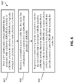
- the method 600 begins at block 602 and includes storing a row number and a column number that are associated with a defective eDRAM of a plurality of defective eDRAMs (e.g., eDRAMs 402 ).
- a system 300 may be configured to detect defective or inoperable eDRAMs 402 via conventional methods that track errors in the hardware (e.g., manufacturing testing, error detection performed by ECC logic of fetch and error correction circuitry 408 , and other such methods).
- data stored in a failing location i.e., a defective eDRAM
- the plurality of eDRAMs 402 can be logically arranged in a plurality of rows and a plurality of columns.
- the plurality of eDRAMs 402 may include 235 eDRAMS 402 , the plurality of rows may include 5 rows and the plurality of columns may include 47 columns, as is shown in for example, FIGS. 4A and 4B .
- the row and column numbers that are associated with the defective eDRAM can be stored in registers, such as a Row of Defective eDRAM (RDE) register and Column of Defective eDRAM (CDE) register, respectively.
- RDE Row of Defective eDRAM
- CDE Column of Defective eDRAM
- registers may be specific to every cache bank 400 and can be contained within control logic (not shown) that is part of the cache bank 400 (e.g., in the L4 cache 220 ).
- the stored row number and column number may be accessed by one or more controllers that can use the stored row number and column number to determine whether to activate one or more column shifters 502 , 504 and which column shifters 502 , 504 to activate.
- the method includes receiving a command to access a cache line.
- the cache line may correspond to a selected row of eDRAMs 402 the plurality of eDRAMs 402 .
- the command may be, for example, a store command for storing data in cache associated with a row of the plurality of eDRAMs 402 or a fetch command for fetching data from a cache associated with a row of the plurality of eDRAMs 402 .
- the L4 cache 220 may perform access operations based on store and fetch commands that result from instructions performed by a processor.
- the cache controller there may request the cache line containing the operand from L2 cache 308 . If the cache line is not present in L2 cache 308 , the cache controller there may request the line from the shared L3 cache 314 . If the cache line is not present in the L3 cache 314 , the cache controller there (e.g., labeled as memory controller), may request the line from the L4 cache 220 in the SC chip 110 .
- the cache controller in the L4 cache 220 may receive a cache line fetch request, which may be a command that is received over the bus connecting the SC chip 110 to the CP chip 122 a . If the L4 cache 220 does not have the line, it may send commands to the other SC chips in the system to query their caches, which is likewise received by the other SC chips as a fetch command arriving over a bus.
- the method includes, in response to determining that the selected row matches the row number that is associated with the defective eDRAM, activating one or more column shifters to prevent access to the defective eDRAM and provide access to a spare eDRAM when accessing the cache line.
- the system may compare the selected row to the row of the defective eDRAM stored by the RDE register to determine if they are the same. If the RDE register is empty (i.e., no defective eDRAM of the bank 400 has been previously identified) or a row number other than row number associated with the selected row is stored by the register, then the system will determine that there is no match.
- every cache access operation may include accessing the RDE and CDE registers to determine if there is a defective eDRAM 402 and determine whether column shifting should be utilized.
- the activation of the one or more column shifters may be based on the column number that is associated with the defective eDRAM. In other words, the selection of how many and which column shifters are to be activated can depend on the column number stored by the CDE register.
- the spare eDRAM 404 provided in association with the plurality of eDRAMs 402 may be the only spare eDRAM 404 available for use in association with the plurality of eDRAMs 402 .
- providing a single spare eDRAM 404 can provide significant savings in terms of available resources as compared with, for example, providing an entire column or row of spare eDRAMs.
- a column shifter (e.g., store column shifter 502 or fetch column shifter 504 ) may be a multiplexer configured to receive a first symbol provided by eDRAMs 402 of a first column of the plurality of columns and a second symbol provide by eDRAMs 402 of a second column of the plurality of columns. As shown, the second column is logically adjacent to the first column.
- the one or more column shifters 502 , 504 can be dynamically controlled (i.e., selectively activated and deactivated) by control logic associated with bank 400 and/or plurality of eDRAMs 402 based on the selected row of eDRAMs 402 corresponding to the cache line and the stored row number and column number that are associated with a defective eDRAM 402 .
- the one or more column shifters 502 , 504 can be dynamically controlled (i.e., activated and deactivated) by one or more controllers of bank 400 based on the selected row of eDRAMs 402 corresponding to the cache line and the stored row number and column number that are associated with a defective eDRAM 402 .
- the command may be a store command and activating one or more column shifters to prevent access to the defective eDRAM 402 and provide access to the spare eDRAM 404 can include for each column of the plurality of columns, activating a store column shifter 502 associated with the column in response to determining that a number of the column is greater than the column number that is associated with the defective eDRAM 402 .
- the method may further include storing data in the spare eDRAM 404 .
- the command may be a fetch command and activating one or more column shifters to prevent access to the defective eDRAM 402 and provide access to the spare eDRAM 404 includes for each column of the plurality of columns, activating a fetch column shifter 504 associated with the column in response to determining that a number of the column is greater than or equal to the column number that is associated with the defective eDRAM 402 .
- the method may further include fetching data from the spare eDRAM 404 .
- one only internal eDRAM row (e.g., out of 4096 internal rows) is accessed within each eDRAM 402 of one of the rows of the plurality of eDRAMs 402 (e.g., one of rows A, B, C, D or E).
- the method may further include receiving a different command to access a different cache line.
- the different cache line may correspond to a different row of eDRAMs 402 of the plurality of eDRAMs 402 .
- the method may also include abstaining from activating any column shifters 502 , 504 .
- a command to access a cache line references a cache line that is in a different row of eDRAMs 402 than the row number that is associated with the defective eDRAM (e.g., based on a comparison to the value stored by the CDE register), then the system may access the cache line in the row of eDRAMs 402 without utilizing any of the column shifters.
- the present invention may be a system, a method, and/or a computer program product at any possible technical detail level of integration
- the computer program product may include a computer readable storage medium (or media) having computer readable program instructions thereon for causing a processor to carry out aspects of the present invention
- the computer readable storage medium can be a tangible device that can retain and store instructions for use by an instruction execution device.
- the computer readable storage medium may be, for example, but is not limited to, an electronic storage device, a magnetic storage device, an optical storage device, an electromagnetic storage device, a semiconductor storage device, or any suitable combination of the foregoing.
- a non-exhaustive list of more specific examples of the computer readable storage medium includes the following: a portable computer diskette, a hard disk, a random access memory (RAM), a read-only memory (ROM), an erasable programmable read-only memory (EPROM or Flash memory), a static random access memory (SRAM), a portable compact disc read-only memory (CD-ROM), a digital versatile disk (DVD), a memory stick, a floppy disk, a mechanically encoded device such as punch-cards or raised structures in a groove having instructions recorded thereon, and any suitable combination of the foregoing.
- RAM random access memory
- ROM read-only memory
- EPROM or Flash memory erasable programmable read-only memory
- SRAM static random access memory
- CD-ROM compact disc read-only memory
- DVD digital versatile disk
- memory stick a floppy disk
- a mechanically encoded device such as punch-cards or raised structures in a groove having instructions recorded thereon
- a computer readable storage medium is not to be construed as being transitory signals per se, such as radio waves or other freely propagating electromagnetic waves, electromagnetic waves propagating through a waveguide or other transmission media (e.g., light pulses passing through a fiber-optic cable), or electrical signals transmitted through a wire.
- Computer readable program instructions described herein can be downloaded to respective computing/processing devices from a computer readable storage medium or to an external computer or external storage device via a network, for example, the Internet, a local area network, a wide area network and/or a wireless network.
- the network may comprise copper transmission cables, optical transmission fibers, wireless transmission, routers, firewalls, switches, gateway computers and/or edge servers.
- a network adapter card or network interface in each computing/processing device receives computer readable program instructions from the network and forwards the computer readable program instructions for storage in a computer readable storage medium within the respective computing/processing device.
- Computer readable program instructions for carrying out operations of the present invention may be assembler instructions, instruction-set-architecture (ISA) instructions, machine instructions, machine dependent instructions, microcode, firmware instructions, state-setting data, configuration data for integrated circuitry, or either source code or object code written in any combination of one or more programming languages, including an object oriented programming language such as Smalltalk, C++, or the like, and procedural programming languages, such as the “C” programming language or similar programming languages.
- the computer readable program instructions may execute entirely on the user's computer, partly on the user's computer, as a stand-alone software package, partly on the user's computer and partly on a remote computer or entirely on the remote computer or server.
- the remote computer may be connected to the user's computer through any type of network, including a local area network (LAN) or a wide area network (WAN), or the connection may be made to an external computer (for example, through the Internet using an Internet Service Provider).
- electronic circuitry including, for example, programmable logic circuitry, field-programmable gate arrays (FPGA), or programmable logic arrays (PLA) may execute the computer readable program instruction by utilizing state information of the computer readable program instructions to personalize the electronic circuitry, in order to perform aspects of the present invention.
- These computer readable program instructions may be provided to a processor of a general purpose computer, special purpose computer, or other programmable data processing apparatus to produce a machine, such that the instructions, which execute via the processor of the computer or other programmable data processing apparatus, create means for implementing the functions/acts specified in the flowchart and/or block diagram block or blocks.
- These computer readable program instructions may also be stored in a computer readable storage medium that can direct a computer, a programmable data processing apparatus, and/or other devices to function in a particular manner, such that the computer readable storage medium having instructions stored therein comprises an article of manufacture including instructions which implement aspects of the function/act specified in the flowchart and/or block diagram block or blocks.
- the computer readable program instructions may also be loaded onto a computer, other programmable data processing apparatus, or other device to cause a series of operational steps to be performed on the computer, other programmable apparatus or other device to produce a computer implemented process, such that the instructions which execute on the computer, other programmable apparatus, or other device implement the functions/acts specified in the flowchart and/or block diagram block or blocks.
- each block in the flowchart or block diagrams may represent a module, segment, or portion of instructions, which comprises one or more executable instructions for implementing the specified logical function(s).
- the functions noted in the blocks may occur out of the order noted in the Figures.
- two blocks shown in succession may, in fact, be executed substantially concurrently, or the blocks may sometimes be executed in the reverse order, depending upon the functionality involved.
Landscapes
- Engineering & Computer Science (AREA)
- Theoretical Computer Science (AREA)
- Physics & Mathematics (AREA)
- General Engineering & Computer Science (AREA)
- General Physics & Mathematics (AREA)
- Human Computer Interaction (AREA)
- Quality & Reliability (AREA)
- Computer Security & Cryptography (AREA)
- Memory System Of A Hierarchy Structure (AREA)
Abstract
Description
Claims (20)
Priority Applications (1)
| Application Number | Priority Date | Filing Date | Title |
|---|---|---|---|
| US16/280,577 US11221794B2 (en) | 2019-02-20 | 2019-02-20 | Memory array element sparing |
Applications Claiming Priority (1)
| Application Number | Priority Date | Filing Date | Title |
|---|---|---|---|
| US16/280,577 US11221794B2 (en) | 2019-02-20 | 2019-02-20 | Memory array element sparing |
Publications (2)
| Publication Number | Publication Date |
|---|---|
| US20200264803A1 US20200264803A1 (en) | 2020-08-20 |
| US11221794B2 true US11221794B2 (en) | 2022-01-11 |
Family
ID=72042148
Family Applications (1)
| Application Number | Title | Priority Date | Filing Date |
|---|---|---|---|
| US16/280,577 Active US11221794B2 (en) | 2019-02-20 | 2019-02-20 | Memory array element sparing |
Country Status (1)
| Country | Link |
|---|---|
| US (1) | US11221794B2 (en) |
Citations (20)
| Publication number | Priority date | Publication date | Assignee | Title |
|---|---|---|---|---|
| US4908798A (en) * | 1987-07-20 | 1990-03-13 | Nec Corporation | Semiconductor memory device with memory cell arrays and a redundant memory cell array associated with a small number of write-in and sense amplifying circuits |
| US5574729A (en) * | 1990-09-29 | 1996-11-12 | Mitsubishi Denki Kabushiki Kaisha | Redundancy circuit for repairing defective bits in semiconductor memory device |
| US5742556A (en) * | 1996-12-26 | 1998-04-21 | Micro Magic, Inc. | Redundancy scheme for semiconductor RAMS |
| US20010002176A1 (en) * | 1999-02-12 | 2001-05-31 | Mitsubishi Denki Kabushiki Kaisha | Semiconductor memory device having a large band width and allowing efficient execution of redundant repair |
| US20010028584A1 (en) * | 2000-03-28 | 2001-10-11 | Kabushiki Kaisha Toshiba | Semiconductor memory device having replacing defective columns with redundant columns |
| US6408401B1 (en) | 1998-11-13 | 2002-06-18 | Compaq Information Technologies Group, L.P. | Embedded RAM with self-test and self-repair with spare rows and columns |
| US6765832B1 (en) * | 2003-03-28 | 2004-07-20 | Renesas Technology Corp. | Semiconductor memory device with word line shift configuration |
| US6876557B2 (en) | 2001-06-12 | 2005-04-05 | Ibm Corporation | Unified SRAM cache system for an embedded DRAM system having a micro-cell architecture |
| US6928377B2 (en) | 2003-09-09 | 2005-08-09 | International Business Machines Corporation | Self-test architecture to implement data column redundancy in a RAM |
| US20070030742A1 (en) * | 2005-08-02 | 2007-02-08 | Micron Technology, Inc. | Combination column redundancy system for a memory array |
| US20090067269A1 (en) * | 2007-09-12 | 2009-03-12 | International Business Machines Corporation | Memory column redundancy scheme |
| US7702972B2 (en) | 2007-10-18 | 2010-04-20 | International Business Machines Corporation | Method and apparatus for SRAM macro sparing in computer chips |
| US20100128541A1 (en) * | 2008-11-21 | 2010-05-27 | Russell Andrew C | Integrated circuit having memory with configurable read/write operations and method therefor |
| US20130007544A1 (en) * | 2011-07-01 | 2013-01-03 | Avalanche Technology, Inc. | Mapping of random defects in a memory device |
| US8358548B2 (en) | 2009-10-19 | 2013-01-22 | Avago Technologies Enterprise IP (Singapore) Pte. Ltd. | Methods for efficiently repairing embedded dynamic random-access memory having marginally failing cells |
| US8402326B2 (en) | 2006-06-26 | 2013-03-19 | Micron Technology, Inc. | Integrated circuit having memory array including ECC and column redundancy and method of operating same |
| US8468419B2 (en) | 2009-08-31 | 2013-06-18 | Lsi Corporation | High-reliability memory |
| US8724423B1 (en) | 2012-12-12 | 2014-05-13 | Lsi Corporation | Synchronous two-port read, two-port write memory emulator |
| US9396815B2 (en) | 2009-08-12 | 2016-07-19 | Taiwan Semiconductor Manufacturing Company, Ltd. | Memory structure |
| US20180196709A1 (en) | 2015-12-23 | 2018-07-12 | Intel Corporation | Method and apparatus for partial cache line sparing |
-
2019
- 2019-02-20 US US16/280,577 patent/US11221794B2/en active Active
Patent Citations (20)
| Publication number | Priority date | Publication date | Assignee | Title |
|---|---|---|---|---|
| US4908798A (en) * | 1987-07-20 | 1990-03-13 | Nec Corporation | Semiconductor memory device with memory cell arrays and a redundant memory cell array associated with a small number of write-in and sense amplifying circuits |
| US5574729A (en) * | 1990-09-29 | 1996-11-12 | Mitsubishi Denki Kabushiki Kaisha | Redundancy circuit for repairing defective bits in semiconductor memory device |
| US5742556A (en) * | 1996-12-26 | 1998-04-21 | Micro Magic, Inc. | Redundancy scheme for semiconductor RAMS |
| US6408401B1 (en) | 1998-11-13 | 2002-06-18 | Compaq Information Technologies Group, L.P. | Embedded RAM with self-test and self-repair with spare rows and columns |
| US20010002176A1 (en) * | 1999-02-12 | 2001-05-31 | Mitsubishi Denki Kabushiki Kaisha | Semiconductor memory device having a large band width and allowing efficient execution of redundant repair |
| US20010028584A1 (en) * | 2000-03-28 | 2001-10-11 | Kabushiki Kaisha Toshiba | Semiconductor memory device having replacing defective columns with redundant columns |
| US6876557B2 (en) | 2001-06-12 | 2005-04-05 | Ibm Corporation | Unified SRAM cache system for an embedded DRAM system having a micro-cell architecture |
| US6765832B1 (en) * | 2003-03-28 | 2004-07-20 | Renesas Technology Corp. | Semiconductor memory device with word line shift configuration |
| US6928377B2 (en) | 2003-09-09 | 2005-08-09 | International Business Machines Corporation | Self-test architecture to implement data column redundancy in a RAM |
| US20070030742A1 (en) * | 2005-08-02 | 2007-02-08 | Micron Technology, Inc. | Combination column redundancy system for a memory array |
| US8402326B2 (en) | 2006-06-26 | 2013-03-19 | Micron Technology, Inc. | Integrated circuit having memory array including ECC and column redundancy and method of operating same |
| US20090067269A1 (en) * | 2007-09-12 | 2009-03-12 | International Business Machines Corporation | Memory column redundancy scheme |
| US7702972B2 (en) | 2007-10-18 | 2010-04-20 | International Business Machines Corporation | Method and apparatus for SRAM macro sparing in computer chips |
| US20100128541A1 (en) * | 2008-11-21 | 2010-05-27 | Russell Andrew C | Integrated circuit having memory with configurable read/write operations and method therefor |
| US9396815B2 (en) | 2009-08-12 | 2016-07-19 | Taiwan Semiconductor Manufacturing Company, Ltd. | Memory structure |
| US8468419B2 (en) | 2009-08-31 | 2013-06-18 | Lsi Corporation | High-reliability memory |
| US8358548B2 (en) | 2009-10-19 | 2013-01-22 | Avago Technologies Enterprise IP (Singapore) Pte. Ltd. | Methods for efficiently repairing embedded dynamic random-access memory having marginally failing cells |
| US20130007544A1 (en) * | 2011-07-01 | 2013-01-03 | Avalanche Technology, Inc. | Mapping of random defects in a memory device |
| US8724423B1 (en) | 2012-12-12 | 2014-05-13 | Lsi Corporation | Synchronous two-port read, two-port write memory emulator |
| US20180196709A1 (en) | 2015-12-23 | 2018-07-12 | Intel Corporation | Method and apparatus for partial cache line sparing |
Non-Patent Citations (3)
| Title |
|---|
| Cho et al.,"A Survey of Repair Analysis Algorithms for Memories" ACM Computing Surveys (CSUR), Oct. 2016. vol. 49 Issue 3, Dec. 2016, Article No. 47. 41 pages. DOI: http://dx.doi.org/10.1145/2971481. |
| Jun et al., "Recovering from Biased Distribution of Faulty Cells in Memory by Reorganizing Replacement Regions through Universal Hashing" ACM Transactions on Design Automation of Electronic Systems (TODAES), vol. 23 Issue 2, Jan. 2018, Article No. 16. 21 pages. |
| Namekawa et al., "Dynamically shift-switched dataline redundancy suitable for DRAM macro with wide data bus," IEEE Journal of Solid-State Circuits, May 2000, vol. 35, Issue: 5, pp. 705-712. |
Also Published As
| Publication number | Publication date |
|---|---|
| US20200264803A1 (en) | 2020-08-20 |
Similar Documents
| Publication | Publication Date | Title |
|---|---|---|
| US20210406170A1 (en) | Flash-Based Coprocessor | |
| US7134057B1 (en) | Off-pitch column redundancy using dynamic shifters | |
| US9639458B2 (en) | Reducing memory accesses for enhanced in-memory parallel operations | |
| US7526612B2 (en) | Multiport cache memory which reduces probability of bank contention and access control system thereof | |
| US8527708B2 (en) | Detecting address conflicts in a cache memory system | |
| KR20060049710A (en) | An apparatus and method for partitioning a shared cache of a chip multi-processor | |
| JP5039913B2 (en) | Direct storage using a locking cache | |
| US20080270703A1 (en) | Method and system for managing memory transactions for memory repair | |
| US20140223445A1 (en) | Selecting a Resource from a Set of Resources for Performing an Operation | |
| KR102208835B1 (en) | Method and apparatus for reverse memory sparing | |
| US10877755B2 (en) | Processor load using a bit vector to calculate effective address | |
| JPH10301846A (en) | Functional bypass method and system for cache array defect using restoration mask | |
| US7809890B2 (en) | Systems and methods for increasing yield of devices having cache memories by inhibiting use of defective cache entries | |
| KR100297914B1 (en) | Multiple Cache Directories for Snooping Devices | |
| US8036061B2 (en) | Integrated circuit with multiported memory supercell and data path switching circuitry | |
| US8560891B2 (en) | EDRAM macro disablement in cache memory | |
| US5890221A (en) | Method and system for offset miss sequence handling in a data cache array having multiple content addressable field per cache line utilizing an MRU bit | |
| US9489255B2 (en) | Dynamic array masking | |
| US9792213B2 (en) | Mitigating busy time in a high performance cache | |
| US20230401153A1 (en) | Processor and method designating an in-core cache of a hierarchical cache system to perform writing-back and invalidation of cached data | |
| US11221794B2 (en) | Memory array element sparing | |
| US10147493B2 (en) | System on-chip (SoC) device with dedicated clock generator for memory banks | |
| WO2019166762A1 (en) | An apparatus and method for accessing metadata when debugging a device | |
| US10402325B2 (en) | Memory system | |
| US7254746B1 (en) | Method and apparatus for using a fault tolerant memory in processor testing and design |
Legal Events
| Date | Code | Title | Description |
|---|---|---|---|
| AS | Assignment |
Owner name: INTERNATIONAL BUSINESS MACHINES CORPORATION, NEW YORK Free format text: ASSIGNMENT OF ASSIGNORS INTEREST;ASSIGNORS:BRONSON, TIM;HUYNH, HIEU T.;KLAPPROTH, KENNETH;REEL/FRAME:048385/0971 Effective date: 20190220 |
|
| FEPP | Fee payment procedure |
Free format text: ENTITY STATUS SET TO UNDISCOUNTED (ORIGINAL EVENT CODE: BIG.); ENTITY STATUS OF PATENT OWNER: LARGE ENTITY |
|
| STPP | Information on status: patent application and granting procedure in general |
Free format text: FINAL REJECTION MAILED |
|
| STPP | Information on status: patent application and granting procedure in general |
Free format text: ADVISORY ACTION MAILED |
|
| STPP | Information on status: patent application and granting procedure in general |
Free format text: NON FINAL ACTION MAILED |
|
| STPP | Information on status: patent application and granting procedure in general |
Free format text: RESPONSE TO NON-FINAL OFFICE ACTION ENTERED AND FORWARDED TO EXAMINER |
|
| STPP | Information on status: patent application and granting procedure in general |
Free format text: FINAL REJECTION MAILED |
|
| STPP | Information on status: patent application and granting procedure in general |
Free format text: RESPONSE AFTER FINAL ACTION FORWARDED TO EXAMINER |
|
| STPP | Information on status: patent application and granting procedure in general |
Free format text: ADVISORY ACTION MAILED |
|
| STPP | Information on status: patent application and granting procedure in general |
Free format text: DOCKETED NEW CASE - READY FOR EXAMINATION |
|
| STPP | Information on status: patent application and granting procedure in general |
Free format text: NOTICE OF ALLOWANCE MAILED -- APPLICATION RECEIVED IN OFFICE OF PUBLICATIONS |
|
| STPP | Information on status: patent application and granting procedure in general |
Free format text: PUBLICATIONS -- ISSUE FEE PAYMENT RECEIVED |
|
| STPP | Information on status: patent application and granting procedure in general |
Free format text: PUBLICATIONS -- ISSUE FEE PAYMENT VERIFIED |
|
| STCF | Information on status: patent grant |
Free format text: PATENTED CASE |