US11221719B2 - Sensor pattern and capacitive touch screen - Google Patents
Sensor pattern and capacitive touch screen Download PDFInfo
- Publication number
- US11221719B2 US11221719B2 US16/049,695 US201816049695A US11221719B2 US 11221719 B2 US11221719 B2 US 11221719B2 US 201816049695 A US201816049695 A US 201816049695A US 11221719 B2 US11221719 B2 US 11221719B2
- Authority
- US
- United States
- Prior art keywords
- sensor element
- type sensor
- cell
- trace
- type
- Prior art date
- Legal status (The legal status is an assumption and is not a legal conclusion. Google has not performed a legal analysis and makes no representation as to the accuracy of the status listed.)
- Active, expires
Links
- 238000010586 diagram Methods 0.000 description 17
- 238000013507 mapping Methods 0.000 description 6
- 238000005457 optimization Methods 0.000 description 2
- 230000004075 alteration Effects 0.000 description 1
- 239000011521 glass Substances 0.000 description 1
- AMGQUBHHOARCQH-UHFFFAOYSA-N indium;oxotin Chemical compound [In].[Sn]=O AMGQUBHHOARCQH-UHFFFAOYSA-N 0.000 description 1
- 238000004519 manufacturing process Methods 0.000 description 1
- 239000007769 metal material Substances 0.000 description 1
- 238000000034 method Methods 0.000 description 1
- 238000012986 modification Methods 0.000 description 1
- 230000004048 modification Effects 0.000 description 1
Images


Classifications
-
- G—PHYSICS
- G06—COMPUTING; CALCULATING OR COUNTING
- G06F—ELECTRIC DIGITAL DATA PROCESSING
- G06F3/00—Input arrangements for transferring data to be processed into a form capable of being handled by the computer; Output arrangements for transferring data from processing unit to output unit, e.g. interface arrangements
- G06F3/01—Input arrangements or combined input and output arrangements for interaction between user and computer
- G06F3/03—Arrangements for converting the position or the displacement of a member into a coded form
- G06F3/041—Digitisers, e.g. for touch screens or touch pads, characterised by the transducing means
- G06F3/044—Digitisers, e.g. for touch screens or touch pads, characterised by the transducing means by capacitive means
- G06F3/0446—Digitisers, e.g. for touch screens or touch pads, characterised by the transducing means by capacitive means using a grid-like structure of electrodes in at least two directions, e.g. using row and column electrodes
-
- G—PHYSICS
- G06—COMPUTING; CALCULATING OR COUNTING
- G06F—ELECTRIC DIGITAL DATA PROCESSING
- G06F3/00—Input arrangements for transferring data to be processed into a form capable of being handled by the computer; Output arrangements for transferring data from processing unit to output unit, e.g. interface arrangements
- G06F3/01—Input arrangements or combined input and output arrangements for interaction between user and computer
- G06F3/03—Arrangements for converting the position or the displacement of a member into a coded form
- G06F3/041—Digitisers, e.g. for touch screens or touch pads, characterised by the transducing means
- G06F3/0416—Control or interface arrangements specially adapted for digitisers
- G06F3/04164—Connections between sensors and controllers, e.g. routing lines between electrodes and connection pads
-
- G—PHYSICS
- G06—COMPUTING; CALCULATING OR COUNTING
- G06F—ELECTRIC DIGITAL DATA PROCESSING
- G06F3/00—Input arrangements for transferring data to be processed into a form capable of being handled by the computer; Output arrangements for transferring data from processing unit to output unit, e.g. interface arrangements
- G06F3/01—Input arrangements or combined input and output arrangements for interaction between user and computer
- G06F3/03—Arrangements for converting the position or the displacement of a member into a coded form
- G06F3/041—Digitisers, e.g. for touch screens or touch pads, characterised by the transducing means
- G06F3/044—Digitisers, e.g. for touch screens or touch pads, characterised by the transducing means by capacitive means
- G06F3/0445—Digitisers, e.g. for touch screens or touch pads, characterised by the transducing means by capacitive means using two or more layers of sensing electrodes, e.g. using two layers of electrodes separated by a dielectric layer
-
- G—PHYSICS
- G06—COMPUTING; CALCULATING OR COUNTING
- G06F—ELECTRIC DIGITAL DATA PROCESSING
- G06F3/00—Input arrangements for transferring data to be processed into a form capable of being handled by the computer; Output arrangements for transferring data from processing unit to output unit, e.g. interface arrangements
- G06F3/01—Input arrangements or combined input and output arrangements for interaction between user and computer
- G06F3/03—Arrangements for converting the position or the displacement of a member into a coded form
- G06F3/041—Digitisers, e.g. for touch screens or touch pads, characterised by the transducing means
- G06F3/044—Digitisers, e.g. for touch screens or touch pads, characterised by the transducing means by capacitive means
- G06F3/0448—Details of the electrode shape, e.g. for enhancing the detection of touches, for generating specific electric field shapes, for enhancing display quality
-
- G—PHYSICS
- G06—COMPUTING; CALCULATING OR COUNTING
- G06F—ELECTRIC DIGITAL DATA PROCESSING
- G06F2203/00—Indexing scheme relating to G06F3/00 - G06F3/048
- G06F2203/041—Indexing scheme relating to G06F3/041 - G06F3/045
- G06F2203/04107—Shielding in digitiser, i.e. guard or shielding arrangements, mostly for capacitive touchscreens, e.g. driven shields, driven grounds
-
- G—PHYSICS
- G06—COMPUTING; CALCULATING OR COUNTING
- G06F—ELECTRIC DIGITAL DATA PROCESSING
- G06F2203/00—Indexing scheme relating to G06F3/00 - G06F3/048
- G06F2203/041—Indexing scheme relating to G06F3/041 - G06F3/045
- G06F2203/04111—Cross over in capacitive digitiser, i.e. details of structures for connecting electrodes of the sensing pattern where the connections cross each other, e.g. bridge structures comprising an insulating layer, or vias through substrate
Definitions
- the present invention relates to a sensor pattern and a capacitive touch screen, and more particularly, to a sensor pattern and a capacitive touch screen capable of simplifying border channel topology to reduce border trace area in a touch screen of an electronic device.
- FIG. 1 is a top view diagram illustrating a transmit (TX)/receive (RX) channel routing of a conventional capacitive TP 100 , wherein the conventional capacitive TP 100 can be a 5.5 inch TP for a smartphone
- FIG. 2 is a simplified block diagram illustrating a pattern 110 and TX/RX mapping of the conventional capacitive TP 100 in FIG.
- the conventional capacitive touch panel 100 comprises 26 TX channels TX 1 ⁇ TX 26 , 15 RX and channels RX 1 ⁇ RX 15 , and the pattern 110 comprises 390 unit blocks 120 .
- Each TX channel comprises 15 TX sensor elements
- each RX channel comprises 26 RX sensor elements.
- Each unit block 120 comprises one TX sensor element and one RX sensor element.
- the conventional capacitive TP 100 requires a larger border area.
- the capacitive TP manufacturers have to upgrade higher level manufacturing equipment to improve width and space of the Ag print, so as to simplify the border area for the capacitive TP application which requires slim border.
- this solution increases the cost a lot.
- a sensor pattern for a capacitive touch screen comprises: a plurality of unit blocks, and a first unit block of the unit blocks comprises: a first 1st-type sensor element, a first 2nd-type sensor element, and a second 2nd-type sensor element.
- the first 1st-type sensor element is disposed on a first patterned layer, having a border trace, two parallel main traces, a bridge, a first cell, and a second cell, wherein the first cell and the second cell are not aligned.
- the bridge is utilized for connecting the first cell and the second cell of the first 1st-type sensor element.
- the first 2nd-type sensor element is disposed on a second patterned layer, having a main trace and a sub-trace, wherein the main trace surrounds the first cell of the first 1st-type sensor element.
- the second 2nd-type sensor element is disposed on the second patterned layer, having a main trace and a sub-trace, wherein the main trace surrounds the second cell of the first 1st-type sensor element.
- a capacitive touch screen comprises a sensor pattern, and the sensor pattern comprises a plurality of unit blocks.
- a first unit block of the unit blocks comprises: a first 1st-type sensor element, a first 2nd-type sensor element, and a second 2nd-type sensor element.
- the first 1st-type sensor element is disposed on a first patterned layer, having a border trace, two parallel main traces, a bridge, a first cell, and a second cell, wherein the first cell and the second cell are not aligned.
- the bridge is utilized for connecting the first cell and the second cell of the first 1st-type sensor element.
- the first 2nd-type sensor element is disposed on a second patterned layer, having a main trace and a sub-trace, wherein the main trace surrounds the first cell of the first 1st-type sensor element.
- the second 2nd-type sensor element is disposed on the second patterned layer, having a main trace and a sub-trace, wherein the main trace surrounds the second cell of the first 1st-type sensor element.
- the sensor pattern and the capacitive touch screen disclosed by the present invention are capable of simplifying border channel topology to reduce border trace area in a touch screen of an electronic device such as a smartphone.
- the slim border Glass-Film-Film (GFF) touch performance optimization can be based on the presented sensor pattern, related IC, and specified algorithm tuning.
- FIG. 1 is a top view diagram illustrating a transmit (TX)/receive (RX) channel routing of a conventional capacitive TP.
- FIG. 2 is a simplified block diagram illustrating a pattern and TX/RX mapping of the conventional capacitive TP in FIG. 1 .
- FIG. 3 is a top view diagram illustrating a transmit (TX)/receive (RX) channel routing of a capacitive touch screen in accordance with a first embodiment of the present invention.
- FIG. 4 is a simplified block diagram illustrating a sensor pattern and TX/RX mapping of the capacitive touch screen in FIG. 3 .
- FIG. 5 is a top view diagram illustrating a transmit (TX)/receive (RX) channel routing of a capacitive touch screen in accordance with a second embodiment of the present invention.
- FIG. 6 is a simplified block diagram illustrating a sensor pattern and TX/RX mapping of the capacitive touch screen in FIG. 5 .
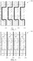
- FIG. 7 is a simplified block diagram illustrating a sensor pattern of the capacitive touch screen in FIG. 5 comprising one type of shielding layer.
- FIG. 8 is a simplified block diagram illustrating a sensor pattern of the capacitive touch screen in FIG. 5 comprising another type of shielding layer.
- FIG. 9 is a simplified block diagram illustrating a sensor pattern of the capacitive touch screen in FIG. 5 comprising two types of shielding layers.
- FIG. 10 is a diagram illustrating another sensor pattern according to an embodiment of the present invention.
- FIG. 3 is a top view diagram illustrating a transmit (TX)/receive (RX) channel routing of a capacitive touch screen 200 in accordance with a first embodiment of the present invention, wherein the capacitive touch screen 200 can be a 5.5 inch touch screen for a smartphone
- FIG. 4 is a simplified block diagram illustrating a sensor pattern 300 and TX/RX mapping of the capacitive touch screen 200 in FIG. 3 .
- the capacitive touch screen 200 comprises 13 TX channels TX 1 ′-TX 13 ′ and 30 RX channels RX 1 ′-RX 30 ′
- the sensor pattern 300 comprises 195 unit blocks UB 1 ⁇ 195 .
- Each TX channel comprises 15 TX sensor elements, and each RX channel comprises 13 RX sensor elements.
- Each unit block of the unit blocks UB 1 ⁇ 195 comprises one TX sensor element and two RX sensor elements.
- the capacitive touch screen 200 requires a smaller border area compared to the conventional capacitive TP 100 .
- the present invention can provide the capacitive touch screen 200 having a number X/2 of TX channels and a number 2*Y of RX channels by using a parallel scheme in the TX pattern and using an alternating scheme in the RX pattern (as shown in FIG. 3 ), so as to simplify the border area and reduce the required border trace area.
- a unit block UB 1 comprises: a first TX sensor element TX 1 a , a first RX sensor element RX 1 a , and a second RX sensor element RX 2 a .
- the first TX sensor element TX 1 a is disposed on a first patterned layer, and has a border trace bt 1 , two parallel main traces m 1 , m 1 ′, a bridge b 1 , a first cell c 1 , and a second cell c 1 ′, wherein the first cell c 1 and the second cell c 1 ′ are not aligned so as to improve touch sensing quality.
- the bridge b 1 is utilized for connecting the first cell c 1 and the second cell c 1 ′ of the first TX sensor element TX 1 a .
- the first RX sensor element RX 1 a is disposed on a second patterned layer, and has a main trace mr 1 a and a sub-trace sr 1 a , wherein the main trace mr 1 a surrounds the first cell c 1 of the first TX sensor element TX 1 a .
- the second RX sensor element RX 2 a is disposed on the second patterned layer, having a main trace mr 2 a and a sub-trace sr 2 a , wherein the main trace mr 2 a surrounds the second cell c 1 ′ of the first TX sensor element TX 1 a .
- a unit block UB 2 comprises: a second TX sensor element TX 2 a , a third RX sensor element RX 1 b , and a fourth RX sensor element RX 2 b .
- the second TX sensor element TX 2 a is disposed on a first patterned layer, and has a border trace bt 2 , two parallel main traces m 2 , m 2 ′, a bridge b 2 , a first cell c 2 , and a second cell c 2 ′, wherein the first cell c 2 and the second cell c 2 ′ are not aligned so as to improve touch sensing quality.
- the bridge b 2 is utilized for connecting the first cell c 2 and the second cell c 2 ′ of the second TX sensor element TX 2 a .
- the third RX sensor element RX 1 b is disposed on a second patterned layer, and has a main trace mr 1 b and a sub-trace sr 1 b , wherein the main trace mr 1 b surrounds the first cell c 2 of the second TX sensor element TX 2 a , and the sub-trace sr 1 b is coupled to the first RX sensor element RX 1 a of the unit block UB 1 .
- the fourth RX sensor element RX 2 b is disposed on the second patterned layer, having a main trace mr 2 b and a sub-trace sr 2 b , wherein the main trace mr 2 b surrounds the second cell c 2 ′ of the second TX sensor element TX 2 a and the sub-trace sr 2 b is coupled to the second RX sensor element RX 2 a of the unit block UB 1 .
- first cell c 1 of the first TX sensor element TX 1 a and the first cell c 2 of the second TX sensor element TX 2 a are aligned
- second cell of c 1 ′ the first TX sensor element TX 1 a and the second cell c 2 ′ of the second TX sensor element TX 2 a are aligned.
- the above embodiment is merely for an illustrative purpose and is not meant to be a limitation of the present invention.
- the number of TX sensor elements in the TX channel and the number of RX sensor elements in the RX channel can be changed according to different design requirements.
- the positions of the TX channels and the RX channels can be swapped.
- FIG. 5 is a top view diagram illustrating a transmit (TX)/receive (RX) channel routing of a capacitive touch screen 400 in accordance with a second embodiment of the present invention, wherein the capacitive touch screen 400 can be a 5.5 inch touch screen for a smartphone
- FIG. 6 is a simplified block diagram illustrating a sensor pattern 500 and TX/RX mapping of the capacitive touch screen 400 in FIG. 5
- the capacitive touch screen 400 comprises 13 TX channels TX 1 ′ ⁇ TX 13 ′ and 30 RX channels RX 1 ′ ⁇ RX 30 ′
- the sensor pattern 500 comprises 195 unit blocks UB 1 ⁇ 195 .
- Each TX channel comprises 15 TX sensor elements, and each RX channel comprises 13 RX sensor elements.
- Each unit block of the unit blocks UB 1 ⁇ 195 comprises one TX sensor element and two RX sensor elements.
- the capacitive touch screen 400 requires a smaller border area compared to the conventional capacitive TP 100 .
- the present invention can provide the capacitive touch screen 400 having a number X/2 of TX channels and a number 2*Y of RX channels by using a parallel scheme in the TX pattern and using an alternating scheme in the RX pattern (as shown in FIG. 5 ), so as to simplify the border area and reduce the required border trace area.
- a unit block UB 1 comprises: a first TX sensor element TX 1 a , a first RX sensor element RX 1 a , and a second RX sensor element RX 2 a .
- the first TX sensor element TX 1 a is disposed on a first patterned layer, and has a border trace bt 1 , two parallel main traces m 1 , m 1 ′, a bridge b 1 , a first cell c 1 , and a second cell c 1 ′, wherein the first cell c 1 and the second cell c 1 ′ are not aligned so as to improve touch sensing quality.
- the bridge b 1 is utilized for connecting the first cell c 1 and the second cell c 1 ‘ of the first TX sensor element TX 1 a .
- the first RX sensor element RX 1 a is disposed on a second patterned layer, and has a main trace mr 1 a and a sub-trace sr 1 a , wherein the main trace mr 1 a surrounds the first cell c 1 of the first TX sensor element TX 1 a .
- the second RX sensor element RX 2 a is disposed on the second patterned layer, having a main trace mr 2 a and a sub-trace sr 2 a , wherein the main trace mr 2 a surrounds the second cell c 1 ’ of the first TX sensor element TX 1 a .
- a unit block UB 2 comprises: a second TX sensor element TX 2 a , a third RX sensor element RX 1 b , and a fourth RX sensor element RX 2 b .
- the second TX sensor element TX 2 a is disposed on a first patterned layer, and has a border trace bt 2 , two parallel main traces m 2 , m 2 ′, a bridge b 2 , a first cell c 2 , and a second cell c 2 ′, wherein the first cell c 2 and the second cell c 2 ′ are not aligned so as to improve touch sensing quality.
- the bridge b 2 is utilized for connecting the first cell c 2 and the second cell c 2 ′ of the second TX sensor element TX 2 a .
- the third RX sensor element RX 1 b is disposed on a second patterned layer, and has a main trace mr 1 b and a sub-trace sr 1 b , wherein the main trace mr 1 b surrounds the second cell c 2 ′ of the second TX sensor element TX 2 a , and the sub-trace sr 1 b is coupled to the first RX sensor element RX 1 a of the unit block UB 1 .
- the fourth RX sensor element RX 2 b is disposed on the second patterned layer, having a main trace mr 2 b and a sub-trace sr 2 b , wherein the main trace mr 2 b surrounds the first cell c 2 of the second TX sensor element TX 2 a and directly connected to the second RX sensor element RX 2 a of the unit block UB 1 .
- first cell clof the first TX sensor element TX 1 a and the second cell c 2 ′ of the second TX sensor element TX 2 a are aligned
- second cell of c 1 ′ the first TX sensor element TX 1 a and the first cell c 2 of the second TX sensor element TX 2 a are aligned.
- the above embodiment is merely for an illustrative purpose and is not meant to be a limitation of the present invention.
- the number of TX sensor elements in the TX channel and the number of RX sensor elements in the RX channel can be changed according to different design requirements.
- the positions of the TX channels and the RX channels can be swapped. For example, FIG.
- FIG. 10 is a diagram illustrating a sensor pattern 300 A, where the first TX sensor element TX 1 a and the second TX sensor element TX 2 a shown in FIG. 4 are replaced with RX sensor elements (e.g. RX 1 a and RX 2 a ), and the first RX sensor element RX 1 a , the second RX sensor element RX 2 a , the third RX sensor element RX 1 b and the fourth RX sensor element RX 2 b shown in FIG. 4 are replaced with TX sensor elements (e.g. TX 1 a , TX 2 a , TX 1 b and TX 2 b ).
- RX sensor elements e.g. RX 1 a and RX 2 a
- the sensor pattern 500 can further comprise a shielding layer 510 as shown in FIG. 7 so as to improve touch sensing quality.
- the shielding layer 510 is disposed between the first RX sensor element RX 1 a and the second RX sensor element RX 2 a and disposed between the third RX sensor element RX 1 b and the fourth RX sensor element RX 2 b .
- the sensor pattern 500 can further comprise a shielding layer 520 as shown in FIG. 8 so as to improve touch sensing quality.
- the shielding layer 520 is disposed between the unit blocks (or the sensor elements) in different columns.
- the sensor pattern 500 also can further comprise both the shielding layer 510 and the shielding layer 520 as shown in FIG. 9 so as to improve touch sensing quality.
- the sensor pattern and the capacitive touch screen disclosed by the present invention are capable of simplifying border channel topology to reduce border trace area in a touch screen of an electronic device such as a smartphone.
- the slim border Glass-Film-Film (GFF) touch performance optimization can be based on the presented sensor pattern, related IC, and specified algorithm tuning.
Landscapes
- Engineering & Computer Science (AREA)
- General Engineering & Computer Science (AREA)
- Theoretical Computer Science (AREA)
- Human Computer Interaction (AREA)
- Physics & Mathematics (AREA)
- General Physics & Mathematics (AREA)
- Computer Networks & Wireless Communication (AREA)
- Quality & Reliability (AREA)
- Position Input By Displaying (AREA)
Priority Applications (1)
| Application Number | Priority Date | Filing Date | Title |
|---|---|---|---|
| US16/049,695 US11221719B2 (en) | 2017-08-01 | 2018-07-30 | Sensor pattern and capacitive touch screen |
Applications Claiming Priority (2)
| Application Number | Priority Date | Filing Date | Title |
|---|---|---|---|
| US201762539561P | 2017-08-01 | 2017-08-01 | |
| US16/049,695 US11221719B2 (en) | 2017-08-01 | 2018-07-30 | Sensor pattern and capacitive touch screen |
Publications (2)
| Publication Number | Publication Date |
|---|---|
| US20190042024A1 US20190042024A1 (en) | 2019-02-07 |
| US11221719B2 true US11221719B2 (en) | 2022-01-11 |
Family
ID=65229444
Family Applications (1)
| Application Number | Title | Priority Date | Filing Date |
|---|---|---|---|
| US16/049,695 Active 2038-09-15 US11221719B2 (en) | 2017-08-01 | 2018-07-30 | Sensor pattern and capacitive touch screen |
Country Status (3)
| Country | Link |
|---|---|
| US (1) | US11221719B2 (zh) |
| CN (1) | CN109324719B (zh) |
| TW (1) | TWI672625B (zh) |
Families Citing this family (1)
| Publication number | Priority date | Publication date | Assignee | Title |
|---|---|---|---|---|
| US10747384B1 (en) | 2019-08-01 | 2020-08-18 | Stmicroelectronics Asia Pacific Pte Ltd | Single layer capacitive touch matrix |
Citations (20)
| Publication number | Priority date | Publication date | Assignee | Title |
|---|---|---|---|---|
| US20100302201A1 (en) * | 2009-06-02 | 2010-12-02 | Avago Technologies Ecbu (Singapore) Pte. Ltd. | Sensor Patterns for Mutual Capacitance Touchscreens |
| US20120133611A1 (en) * | 2010-01-15 | 2012-05-31 | Cypress Semiconductor Corporation | Asymmetric Sensor Pattern |
| CN202453850U (zh) | 2012-01-06 | 2012-09-26 | 宸鸿科技(厦门)有限公司 | 触控面板 |
| CN103246406A (zh) | 2012-02-02 | 2013-08-14 | 群康科技(深圳)有限公司 | 触控面板及包含触控面板的触控显示装置 |
| US20130305168A1 (en) | 2008-05-12 | 2013-11-14 | Sony Corporation | Information processing apparatus and information processing method |
| US20140022202A1 (en) * | 2012-07-18 | 2014-01-23 | Cypress Semiconductor Corporation | Sensor Array with Edge Pattern |
| CN103913873A (zh) | 2013-08-07 | 2014-07-09 | 上海天马微电子有限公司 | 一种液晶面板、显示装置及其扫描方法 |
| CN103927061A (zh) | 2013-01-16 | 2014-07-16 | 联咏科技股份有限公司 | 电容式触控面板 |
| CN104461207A (zh) | 2014-12-31 | 2015-03-25 | 深圳市华星光电技术有限公司 | 单层电容式触摸屏以及触摸显示装置 |
| TW201523402A (zh) | 2013-12-03 | 2015-06-16 | Himax Tech Ltd | 觸控感測裝置 |
| US20150349773A1 (en) * | 2014-05-29 | 2015-12-03 | Cypress Semiconductor Corporation | Single Layer Touchscreen with Ground Insertion |
| CN105446566A (zh) | 2012-09-21 | 2016-03-30 | 友达光电股份有限公司 | 电容式触控面板 |
| US20160109741A1 (en) * | 2014-10-17 | 2016-04-21 | Raydium Semiconductor Corporation | In-cell touch display system, in-cell touch panel and trace layout thereof |
| CN105760033A (zh) | 2016-02-05 | 2016-07-13 | 上海天马微电子有限公司 | 一种触控屏以及触控显示电子设备 |
| US20170017347A1 (en) * | 2012-02-23 | 2017-01-19 | Cypress Semiconductor Corporation | Touch Sensor Pattern |
| CN106547413A (zh) | 2015-09-21 | 2017-03-29 | 矽创电子股份有限公司 | 电容式触控装置 |
| CN106796475A (zh) | 2014-08-20 | 2017-05-31 | 微晶片科技德国公司 | 用于手势检测及跟踪的电极布置 |
| CN106775145A (zh) | 2015-11-23 | 2017-05-31 | 东友精细化工有限公司 | 触摸传感器 |
| US9891745B2 (en) * | 2014-10-17 | 2018-02-13 | Raydium Semiconductor Corporation | In-cell mutual-capacitive touch panel and trace layout thereof |
| US10055069B2 (en) * | 2014-10-17 | 2018-08-21 | Raydium Semiconductor Corporation | In-cell touch panel and trace layout thereof |
-
2018
- 2018-07-27 TW TW107126080A patent/TWI672625B/zh active
- 2018-07-30 US US16/049,695 patent/US11221719B2/en active Active
- 2018-08-01 CN CN201810863834.3A patent/CN109324719B/zh active Active
Patent Citations (20)
| Publication number | Priority date | Publication date | Assignee | Title |
|---|---|---|---|---|
| US20130305168A1 (en) | 2008-05-12 | 2013-11-14 | Sony Corporation | Information processing apparatus and information processing method |
| US20100302201A1 (en) * | 2009-06-02 | 2010-12-02 | Avago Technologies Ecbu (Singapore) Pte. Ltd. | Sensor Patterns for Mutual Capacitance Touchscreens |
| US20120133611A1 (en) * | 2010-01-15 | 2012-05-31 | Cypress Semiconductor Corporation | Asymmetric Sensor Pattern |
| CN202453850U (zh) | 2012-01-06 | 2012-09-26 | 宸鸿科技(厦门)有限公司 | 触控面板 |
| CN103246406A (zh) | 2012-02-02 | 2013-08-14 | 群康科技(深圳)有限公司 | 触控面板及包含触控面板的触控显示装置 |
| US20170017347A1 (en) * | 2012-02-23 | 2017-01-19 | Cypress Semiconductor Corporation | Touch Sensor Pattern |
| US20140022202A1 (en) * | 2012-07-18 | 2014-01-23 | Cypress Semiconductor Corporation | Sensor Array with Edge Pattern |
| CN105446566A (zh) | 2012-09-21 | 2016-03-30 | 友达光电股份有限公司 | 电容式触控面板 |
| CN103927061A (zh) | 2013-01-16 | 2014-07-16 | 联咏科技股份有限公司 | 电容式触控面板 |
| CN103913873A (zh) | 2013-08-07 | 2014-07-09 | 上海天马微电子有限公司 | 一种液晶面板、显示装置及其扫描方法 |
| TW201523402A (zh) | 2013-12-03 | 2015-06-16 | Himax Tech Ltd | 觸控感測裝置 |
| US20150349773A1 (en) * | 2014-05-29 | 2015-12-03 | Cypress Semiconductor Corporation | Single Layer Touchscreen with Ground Insertion |
| CN106796475A (zh) | 2014-08-20 | 2017-05-31 | 微晶片科技德国公司 | 用于手势检测及跟踪的电极布置 |
| US20160109741A1 (en) * | 2014-10-17 | 2016-04-21 | Raydium Semiconductor Corporation | In-cell touch display system, in-cell touch panel and trace layout thereof |
| US9891745B2 (en) * | 2014-10-17 | 2018-02-13 | Raydium Semiconductor Corporation | In-cell mutual-capacitive touch panel and trace layout thereof |
| US10055069B2 (en) * | 2014-10-17 | 2018-08-21 | Raydium Semiconductor Corporation | In-cell touch panel and trace layout thereof |
| CN104461207A (zh) | 2014-12-31 | 2015-03-25 | 深圳市华星光电技术有限公司 | 单层电容式触摸屏以及触摸显示装置 |
| CN106547413A (zh) | 2015-09-21 | 2017-03-29 | 矽创电子股份有限公司 | 电容式触控装置 |
| CN106775145A (zh) | 2015-11-23 | 2017-05-31 | 东友精细化工有限公司 | 触摸传感器 |
| CN105760033A (zh) | 2016-02-05 | 2016-07-13 | 上海天马微电子有限公司 | 一种触控屏以及触控显示电子设备 |
Also Published As
| Publication number | Publication date |
|---|---|
| TWI672625B (zh) | 2019-09-21 |
| CN109324719A (zh) | 2019-02-12 |
| CN109324719B (zh) | 2022-01-18 |
| US20190042024A1 (en) | 2019-02-07 |
| TW201911014A (zh) | 2019-03-16 |
Similar Documents
| Publication | Publication Date | Title |
|---|---|---|
| US10147998B2 (en) | Interface and communication device | |
| JP2024001265A (ja) | 表示装置 | |
| US9030434B2 (en) | Touch display panel and touch sensing unit thereof | |
| US9471167B2 (en) | Organic light-emitting diode touch display panel | |
| US10001889B2 (en) | Mesh electrode, sensing device, and electrode layer | |
| US20180165494A1 (en) | Touch sensor capable of recognizing fingerprints, display device adopting the touch sensor, and electronic device adopting the touch sensor | |
| US20180292693A1 (en) | A display panel and an array substrate thereof | |
| US10579170B2 (en) | Touch control substrate, touch control panel, display substrate, display panel and display device | |
| US20180308902A1 (en) | Oled touch display device | |
| US20110298731A1 (en) | Touch display device and touch display substrate thereof | |
| US20140146004A1 (en) | Input device | |
| US20180210255A1 (en) | Array substrate and touch-sensitive display device | |
| US20220028933A1 (en) | Array substrate and display device | |
| CN108255350B (zh) | 触控显示装置 | |
| CN106371649A (zh) | 内嵌式触控面板 | |
| US8803843B2 (en) | Touch panel and touch sensing method thereof | |
| US10579182B2 (en) | Display substrate, in-cell touch screen and display device | |
| US9013446B2 (en) | Touch sensor mechanism and manufacturing method thereof | |
| US9355807B2 (en) | Touch-sensing liquid crystal panel and fabrication method thereof | |
| US20160190158A1 (en) | Array substrate and display panel | |
| US11221719B2 (en) | Sensor pattern and capacitive touch screen | |
| CN108807715B (zh) | 触控显示面板 | |
| US10152130B2 (en) | Touch apparatus | |
| US9645671B2 (en) | Array substrate, display panel and display device | |
| JP6290271B2 (ja) | インセル型タッチ表示パネル |
Legal Events
| Date | Code | Title | Description |
|---|---|---|---|
| FEPP | Fee payment procedure |
Free format text: ENTITY STATUS SET TO UNDISCOUNTED (ORIGINAL EVENT CODE: BIG.); ENTITY STATUS OF PATENT OWNER: LARGE ENTITY |
|
| STPP | Information on status: patent application and granting procedure in general |
Free format text: DOCKETED NEW CASE - READY FOR EXAMINATION |
|
| STPP | Information on status: patent application and granting procedure in general |
Free format text: NON FINAL ACTION MAILED |
|
| STPP | Information on status: patent application and granting procedure in general |
Free format text: RESPONSE TO NON-FINAL OFFICE ACTION ENTERED AND FORWARDED TO EXAMINER |
|
| STPP | Information on status: patent application and granting procedure in general |
Free format text: FINAL REJECTION MAILED |
|
| STPP | Information on status: patent application and granting procedure in general |
Free format text: RESPONSE AFTER FINAL ACTION FORWARDED TO EXAMINER |
|
| STPP | Information on status: patent application and granting procedure in general |
Free format text: NOTICE OF ALLOWANCE MAILED -- APPLICATION RECEIVED IN OFFICE OF PUBLICATIONS |
|
| AS | Assignment |
Owner name: HIMAX TECHNOLOGIES LIMITED, TAIWAN Free format text: ASSIGNMENT OF ASSIGNORS INTEREST;ASSIGNORS:TSAI, CHENG-HUNG;LIU, YING-ZHUAN;CHEN, YUAN-TING;AND OTHERS;SIGNING DATES FROM 20180723 TO 20180806;REEL/FRAME:058174/0274 |
|
| STPP | Information on status: patent application and granting procedure in general |
Free format text: PUBLICATIONS -- ISSUE FEE PAYMENT VERIFIED |
|
| STCF | Information on status: patent grant |
Free format text: PATENTED CASE |
|
| MAFP | Maintenance fee payment |
Free format text: PAYMENT OF MAINTENANCE FEE, 4TH YEAR, LARGE ENTITY (ORIGINAL EVENT CODE: M1551); ENTITY STATUS OF PATENT OWNER: LARGE ENTITY Year of fee payment: 4 |