US11221361B2 - Controlling power dissipation in an output stage of a test channel - Google Patents
Controlling power dissipation in an output stage of a test channel Download PDFInfo
- Publication number
- US11221361B2 US11221361B2 US16/559,267 US201916559267A US11221361B2 US 11221361 B2 US11221361 B2 US 11221361B2 US 201916559267 A US201916559267 A US 201916559267A US 11221361 B2 US11221361 B2 US 11221361B2
- Authority
- US
- United States
- Prior art keywords
- output stage
- voltage
- power dissipation
- channel
- test system
- Prior art date
- Legal status (The legal status is an assumption and is not a legal conclusion. Google has not performed a legal analysis and makes no representation as to the accuracy of the status listed.)
- Active, expires
Links
Images


Classifications
-
- G—PHYSICS
- G01—MEASURING; TESTING
- G01R—MEASURING ELECTRIC VARIABLES; MEASURING MAGNETIC VARIABLES
- G01R31/00—Arrangements for testing electric properties; Arrangements for locating electric faults; Arrangements for electrical testing characterised by what is being tested not provided for elsewhere
- G01R31/28—Testing of electronic circuits, e.g. by signal tracer
- G01R31/2832—Specific tests of electronic circuits not provided for elsewhere
- G01R31/2836—Fault-finding or characterising
- G01R31/2839—Fault-finding or characterising using signal generators, power supplies or circuit analysers
-
- G—PHYSICS
- G01—MEASURING; TESTING
- G01R—MEASURING ELECTRIC VARIABLES; MEASURING MAGNETIC VARIABLES
- G01R19/00—Arrangements for measuring currents or voltages or for indicating presence or sign thereof
- G01R19/10—Measuring sum, difference or ratio
-
- G—PHYSICS
- G01—MEASURING; TESTING
- G01R—MEASURING ELECTRIC VARIABLES; MEASURING MAGNETIC VARIABLES
- G01R19/00—Arrangements for measuring currents or voltages or for indicating presence or sign thereof
- G01R19/165—Indicating that current or voltage is either above or below a predetermined value or within or outside a predetermined range of values
- G01R19/16566—Circuits and arrangements for comparing voltage or current with one or several thresholds and for indicating the result not covered by subgroups G01R19/16504, G01R19/16528, G01R19/16533
-
- G—PHYSICS
- G01—MEASURING; TESTING
- G01R—MEASURING ELECTRIC VARIABLES; MEASURING MAGNETIC VARIABLES
- G01R31/00—Arrangements for testing electric properties; Arrangements for locating electric faults; Arrangements for electrical testing characterised by what is being tested not provided for elsewhere
- G01R31/28—Testing of electronic circuits, e.g. by signal tracer
- G01R31/317—Testing of digital circuits
- G01R31/31712—Input or output aspects
- G01R31/31715—Testing of input or output circuits; test of circuitry between the I/C pins and the functional core, e.g. testing of input or output driver, receiver, buffer
Definitions
- This specification describes example implementations of a test system configured to control power dissipation in an output stage of a test channel.
- Test systems are configured to test the operation of electronic devices, such as microprocessors and memory chips. Testing may include sending signals to a device and determining how the device reacted to those signals based on its response. For example, testing may include forcing voltage and current onto a test channel and receiving signals from the device based on the forced voltage and current. The device's reaction will dictate whether the device has passed or failed testing.
- An example test system includes an output stage to source at least one of voltage or current to a channel of a test instrument; a tracking circuit to detect a channel voltage following the output stage and to control a supply voltage to the output stage based on the channel voltage; and a controller to determine a power dissipation of the output stage based on the supply voltage and the channel voltage, and to control the output stage based on the power dissipation in the output stage.
- the example test system may include one or more of the following features, either alone or in combination.
- Controlling the supply voltage may include adjusting the supply voltage to track variations in the channel voltage.
- the output stage may operate based on an overhead voltage.
- Controlling the supply voltage may include limiting the supply voltage to a value that is based on a sum of the channel voltage and the overhead voltage. The value of the supply voltage may be equal to the sum of the channel voltage and the overhead voltage.
- the example test system may include a current sensor to detect an output current from the output stage.
- the controller may include a compensator circuit configured to determine the power dissipation based also on the output current.
- the compensator circuit may be configured to determine the power dissipation by performing operations comprising: obtaining a difference voltage between the supply voltage and the channel voltage, and obtaining a product of the output current and the difference voltage.
- the compensator circuit may be configured to determine the power dissipation over time and to determine whether the power dissipation is acceptable for the time.
- the output stage may be controlled based on whether the power dissipation is acceptable for the time.
- the compensator circuit may be configured to control the output stage by interrupting operation of the output stage in response to the power dissipation exceeding an acceptable limit for a period of time.
- the compensator circuit may be configured to compare the power dissipation to a predefined power dissipation and, if the power dissipation exceeds the predefined power dissipation, to control the output stage by interrupting operation of the output stage.
- the tracking circuit may be configured to provide an input voltage to the output stage.
- the at least one of voltage or current sourced onto the channel by the test system may be based on the input voltage.
- Controlling the output stage may include changing the input voltage based on the power dissipation.
- the tracking circuit may be configured to change the supply voltage in a duration measured within single or double digit microseconds of the channel voltage being tracked changing.
- the tracking circuit may be configured to control the supply voltage to limit a voltage differential between the supply voltage and the channel voltage.
- the voltage sourced may be at least 100 volts and the current sourced may be at least 2 amperes pulsed.
- a size of the output stage may be proportional to a difference between the supply voltage and the channel voltage at a maximum current through the output stage. A reduction in a difference between the supply voltage and the channel voltage at the maximum current may enable a reduction in a size of the output stage. The smaller the output stage is in size, the less power dissipation that the output stage will tolerate.
- a maximum power dissipation of the output stage may be based on the supply voltage, the channel voltage, and a current from the output stage.
- An example test system includes test instruments to send signals to, and to receive signals from, a device under test (DUT).
- Each test instrument may include one or more channels.
- a channel among the one or more channels may include an output stage to source at least one of voltage or current.
- a device interface board (DIB) may be for connecting one or more of the test instruments to the DUT both electrically and mechanically.
- a computing system may be configured—for example, programmed—to control operation of one or more of the test instruments.
- the channel may include a tracking circuit to limit a voltage differential between a supply voltage to the output stage and a channel voltage on the channel; and a controller to control the output stage based on a power dissipation in the output stage.
- the example test system may include one or more of the following features, either alone or in combination.
- the output stage may be configured to receive an input voltage and to source at least one of the voltage or the current based on the input voltage.
- the controller may be configured to control the output stage by changing the input voltage.
- the controller may include a compensator circuit that is configured to determine the power dissipation in the output stage by performing operations comprising: obtaining a difference voltage between the supply voltage and the channel voltage, and obtaining a product of the difference voltage and a channel current on the channel.
- the controller may be configured to determine the power dissipation over time and to determine whether the power dissipation is acceptable for the time.
- the controller may be configured to control the output stage based on whether the power dissipation is acceptable.
- the controller may be configured to control the output stage by interrupting operation of the output stage in response to the power dissipation exceeding an acceptable limit for a period of time.
- the controller may be configured to compare the power dissipation to a predefined power dissipation and, if the power dissipation exceeds the predefined power dissipation, to control the output stage by interrupting operation of the output stage.
- Interrupting operation of the output stage may include adjusting input of voltage to the output stage from the controller.
- a size of the output stage may be proportional to a difference between the supply voltage and the channel voltage at a maximum current through the output stage.
- a reduction in a difference between the supply voltage and the channel voltage at the maximum current may enable a reduction in a size of the output stage. The smaller the output stage is in size, the less power dissipation that the output stage will tolerate, with a maximum power dissipation of the output stage being based on the supply voltage, the channel voltage, and a current from the output stage.
- test systems and processes described in this specification may be configured or controlled by executing, on one or more processing devices, instructions that are stored on one or more non-transitory machine-readable storage media.
- non-transitory machine-readable storage media include read-only memory, an optical disk drive, memory disk drive, and random access memory.
- At least part of the test systems and processes described in this specification may be configured or controlled using a computing system comprised of one or more processing devices and memory storing instructions that are executable by the one or more processing devices to perform various control operations.
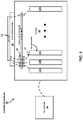
- FIG. 1 is a block diagram of an example test system.
- FIG. 2 is a block diagram of components included in an example test channel of the test system of FIG. 1 .
- FIG. 3 is a flowchart showing operations in an example process for controlling power dissipation in an output stage of the test channel.
- a test channel includes the physical medium or media over which signals are sent from a test system to a device under test (DUT) and over which signals are received from the DUT.
- the test channel includes electrically-conductive media at least part-way between the test system and the DUT.
- the test channel may also include wireless media or optical media part-way between the test system and the DUT.
- Each example test channel includes an output stage.
- the output stage includes power amplifier circuitry—also referred to herein as “power amplifier”—to force voltage (V) and current (I) to the test channel.
- V power amplifier
- I current
- a controller is configured to provide input to the output stage to control the amount of voltage or current that the output stage provides to the test channel based on the user's specifications. Examples of the controller include a compensator circuit, which may be or include an analog compensator circuit or a digital compensator circuit.
- the output stage also receives a supply voltage.
- the supply voltage includes a voltage that powers the output stage.
- the supply voltage is different from the received input used to control the voltage or current output to the test channel.
- the physical size of the output stage is proportional to the power dissipation in the output stage.
- the power dissipation in the output stage is based on a difference between the supply voltage provided to the output stage and a voltage on the test channel provided by the output stage at a maximum current from the output stage. Maximum current is used in this calculation because that results in a maximum power dissipation that should be supported by the output stage for different voltages.
- the magnitude of the supply voltage was set to accommodate a large range of voltage and current outputs by the output stage.
- the supply voltage for an output stage might be 110 volts (V).
- the output stage may need to be controlled to output only 2V onto the test channel.
- the power dissipation in the output stage is based on the difference between 110V and 2V.
- the current through the output stage is 1 ampere (A)
- the power dissipation in the output stage is (110V ⁇ 2V)*(1 A), which is 108 watts (W).
- the output stage was made relatively large. Output stages that are greater in size can support greater power dissipations.
- the output stage may occupy an area of 1000 square millimeters (mm 2 ) on a printed circuit board (PCB) connected to the test channel.
- PCB printed circuit board
- the example test system described herein employs a tracking circuit to detect an output voltage provided by the output stage and to control a supply voltage to the output stage based on the output voltage.
- the tracking circuit is or includes an envelope tracker that detects the channel voltage following the output stage and that adjusts the supply voltage to the output stage. The detecting and adjusting are performed at a rapid rate, thereby enabling the envelope tracker and the output stage to react quickly enough to limit output stage power dissipation duration.
- the detecting and adjusting may be performed in single digit microseconds ( ⁇ s) or in double digit microseconds ( ⁇ s).
- the envelope tracker may detect 2V on the test channel at or following the output of the output stage.
- the envelope tracker within the span of single or double digit microseconds in some examples, adjusts the supply voltage in order to reduce the power dissipation in the output stage.
- the envelope tracker may change the supply voltage from 110V to 6.5V.
- 6.5V of supply voltage is required for the output stage to provide 2V on the test channel.
- the power dissipation in the output stage is (6.5V ⁇ 2V)*(1 A) (where 1 A is the maximum current output from the output stage). So, the power dissipation in the output stage is 4.5 W. The magnitude of this dissipation is considerably less than the 108 W produced in the example above. As a result, the size of the output stage can be reduced relative to the 108 W example. In some implementation, the output stage can be reduced in size to about 50 mm 2 ; however, any appropriate size reductions may be achieved.
- the output stage is programmed to output 90V onto the test channel.
- the envelope tracker may detect 90V on the test channel at or following the output of the output stage.
- the envelope tracker within the span of single or double digit microseconds, adjusts the supply voltage in order to reduce the power dissipation in the output stage.
- the envelope tracker may change the supply voltage from 110V to 94.5V.
- the overhead voltage may not be the same for all channel voltages; however, for this example, the overhead voltage is assumed to be 4.5V.
- a 94.5V supply voltage is required for the output stage to provide 90V on the test channel.
- the power dissipation in the output stage is (94.5V ⁇ 90V)*(1 A) (where 1 A is the maximum current as above). So, the power dissipation in the output stage remains 4.5 W even though a larger voltage output is used.
- the size of the output stage can stay the same or similar for channel voltage magnitudes within a wide range. So, by adjusting the supply voltage, the size of the output stage can be reduced without reducing the range of voltage outputs that the test system can provide. In other words, a reduction in a difference between the supply voltage and the channel voltage at the maximum current enables a reduction in a size of the output stage.
- Reductions in the size of the output stage can have consequences. For example, smaller-sized output stages can be more susceptible to damage than larger-sized output stages. As explained previously, an output stage that is reduced in size, can handle less power dissipation. Generally, the smaller the output stage is in size, the less power dissipation that the output stage can tolerate. In an example, an accidental short circuit may result in a spike in voltage applied to the output stage. As a result, the power dissipation in the output stage may increase beyond that which the output stage can accommodate without failing.
- the compensator circuit is configured to compare the power dissipation in the output stage to a predefined power dissipation and, if the power dissipation in the output stage exceeds the predefined power dissipation, to control the output stage by, for example, changing the input to the output stage or by interrupting operation of the output stage.
- the compensator circuit may be configured—e.g., programmed, structured, or both programmed and structured—to determine the power dissipation in the output stage by obtaining a difference between the supply voltage and a channel voltage on the test channel, and by obtaining the power dissipation based on this difference.
- the compensator circuit may be configured to control the output stage based on the power dissipation within single digit microseconds, for example, within 1 ⁇ s. In some examples, the compensator circuit may be configured to control the output stage based on the power dissipation within double digit microseconds
- FIG. 1 shows components of example automatic test equipment (ATE) 10 that is configured to control power dissipation in an output stage of a test channel using the example techniques described herein.
- ATE automatic test equipment
- the techniques described herein are not limited to use with the ATE of FIG. 1 or to use in testing applications, but rather may be used in any appropriate technical context.
- the dashed lines represent possible signal paths between devices and not actual wiring.
- ATE 10 includes a test head 11 and a test computer 12 .
- Test head 11 interfaces to the DUTs (not shown) on which tests are performed.
- Test computer 12 communicates with test head 11 to control testing. For example, test computer may download test program sets to test instruments on the test head, which then run the test program sets to test DUTs in communication with the test head.
- Computer 12 may also present users with options to set the voltage and current on a test channel.
- multiple test channels for example, each test channel—may include an instance of the output stage power amplifier circuitry, one or more processing devices dedicated to that test channel, or both an instance of the output stage power amplifier circuitry and one or more dedicated processing devices. Examples of types of processing devices that may be used are described herein.
- test instruments 13 A to 13 N include test instruments 13 A to 13 N.
- the test instruments are VI (voltage-current) test instruments configured to force direct current (DC) voltage and to force DC current onto a test channel and to receive signals from the device based on the forced DC voltage and forced DC current.
- VI test instruments may be used in lieu of, or in addition to, VI test instruments.
- test instruments may be used that are configured to produce alternating current (AC) voltage and/or AC current signals having frequencies that are greater than 1 kilohertz (KHZ).
- Each test instrument may be configured to output test signals to test a DUT, and to receive signals from the DUT.
- the signals received may include response signals that are based on the test signals and/or signals that originate from the DUT that are not prompted by (e.g., are not in response to) test signals.
- a test channel may include the physical transmission medium or media over which signals are sent from the test instrument to a DUT and over which signals are received from the DUT.
- Physical transmission media may include, but are not limited to, electrical conductors alone or in combination with optical conductors, wireless transmission media, or both optical conductors and wireless transmission media.
- a test channel may include a range of frequencies over which signals are transmitted over one or more physical transmission media.
- ATE 10 includes a connection interface 14 that connects test instrument test channels 15 to a DIB 16 .
- Connection interface 14 may include connectors 20 or other devices for routing signals between the test instruments and DIB 16 .
- the connection interface may include one or more circuit boards or other substrates on which such connectors are mounted. Conductors that define the instrument test channels may be routed through the connection interface and the DIB.
- DIB 16 connects, electrically and mechanically, to test head 11 .
- the DIB includes sites 21 , which may include pins, conductive traces, or other points of electrical and mechanical connection to which DUTs may connect. Test signals, response signals, and other signals pass via the test channels over the sites between the DUT and test instruments.
- DIB 16 also includes, among other things, connectors, conductive traces, and circuitry for routing signals between the test instruments, DUTs connected to sites 21 , and other circuitry.
- FIG. 2 shows example of components that may be included in the output stage of an example test channel 60 , which may be a test channel that is part of and/or connected to test instrument 13 A for example.
- test channel 60 includes output stage 61 .
- the output stage may include a power amplifier configured to force voltage and current to the transmission media portion 64 of the test channel.
- the test channel also includes one or more processing devices 65 configured to control the output stage as described herein.
- the processing devices may implement a controller, such as a digital compensator circuit, to control the output stage to produce programmed voltage or current on the test channel and/or to adjust or to interrupt operation of the output stage in response to an unsustainable power dissipation in the output stage.
- the digital compensator circuit implements or includes a proportional-integral-derivative (PID) control loop to control operation of the output stage.
- PID proportional-integral-derivative
- the digital compensator circuit implements or includes feed-forward components making it not solely a PID control loop.
- Voltage regulator 67 provides a voltage on which the supply voltage is based.
- the voltage regular may be a static voltage that is capable of outputting only a single DC voltage or a programmable voltage source that is capable of being programmed to provide one or more voltages within a range of voltages.
- the voltage regulator may supply a high voltage, such as 110V, or any other appropriate voltage.
- Tracking circuit 76 may be or include an envelope tracker configured to track voltage (Vd) on the test channel and to control the supply voltage to the output stage based on that voltage.
- the tracking circuit may control the supply voltage (V+) by adjusting the voltage from the voltage regulator.
- the voltage from the voltage regulator may be adjusted by the tracking circuit to a value that is greater than or equal to a sum of channel voltage Vd and the overhead voltage of the output stage.
- the envelope tracker may be configured to limit or to minimize a voltage differential between the supply voltage V+ and the channel voltage Vd on the test channel while maintaining the necessary overhead voltage for operation of the output stage.
- the envelope tracker may limit or minimize the voltage differential by detecting the voltage on the test channel (Vd) 77 and by adjusting the voltage provided by the voltage regulator to produce the supply voltage (V+) 78 .
- the resulting supply voltage is greater than or equal to the sum of the voltage (Vd) on the test channel (for example, the channel voltage following the output stage) and the overhead voltage of the output stage. Keeping the supply voltage close to this sum limits or minimizes the power dissipation in the output stage, thereby enabling use of an output stage that has a smaller or minimized size.
- the envelope tracker may also control the supply voltage by adjusting the supply voltage to track variations in the channel voltage. By doing this, the envelope tracker may reduce or minimize the difference between the channel voltage and the supply voltage for different channel voltages, thereby reducing, minimizing, or keeping consistent the output stage's power dissipation.
- the envelope tracker may take into account the voltage drop across resistor 72 and/or any other voltage drops on the test channel when controlling the supply voltage. For example, the envelope tracker may determine the voltage at point 75 by adding to Vd the voltage drop that occurred across resistors and other voltage drops that occurred before the point at which Vd is measured. In some implementations, the envelope tracker may detect the voltage Vd directly at point 75 rather than after resistor 72 . As noted, the envelope tracker also takes the overhead voltage of the output stage into account when setting the supply voltage. Generally, the larger the difference is between the channel voltage and the supply voltage, the large the size that the output stage will be.
- the tracking circuit for example, the envelope tracker—may be implemented using a buck regulator that tracks the channel voltage and that updates the supply voltage within a time span measured in single digit microseconds, for example, 1 ⁇ s, 2 ⁇ s, 3 ⁇ s, 4 ⁇ s, 5 ⁇ s, 6 ⁇ s, 7 ⁇ s, 8 ⁇ s, or 9 ⁇ s.
- Speeds such as this may be implemented in a buck regulator by using inductors having relatively large inductances and a capacitor having a relatively small capacitance.
- the tracking circuit for example, the envelope tracker—may be implemented using a buck regulator that tracks the channel voltage and that updates the supply voltage within a time span measured in double digit microseconds, for example, 10 ⁇ s, 20 ⁇ s, 30 ⁇ s, 40 ⁇ s, 50 ⁇ s, 60 ⁇ s, 70 ⁇ s, 80 ⁇ s, 90 ⁇ s or any appropriate time span that is less than 100 ⁇ s.
- a buck regulator that tracks the channel voltage and that updates the supply voltage within a time span measured in double digit microseconds, for example, 10 ⁇ s, 20 ⁇ s, 30 ⁇ s, 40 ⁇ s, 50 ⁇ s, 60 ⁇ s, 70 ⁇ s, 80 ⁇ s, 90 ⁇ s or any appropriate time span that is less than 100 ⁇ s.
- the power dissipation in the output stage 61 is equal to or proportional (“ ⁇ ”) to the following voltages and current shown in the figure.
- a user may select or program a voltage to output and the test system may automatically determine a current based on that voltage. And, in some implementations, the user may select the current and the system may automatically determine the voltage.
- the compensator circuit may then control the power amplifier, the envelope tracker, or both, to force the voltage and current to the test channel.
- V+ is adjusted by the envelope tracker based on the voltage that the envelope tracker detects on the test channel—in this example, Vd.
- the compensator circuit may be part of a control loop that includes the envelope tracker, the output stage, voltage sensors, and current sensors.
- the output stage may be configured for control by compensator circuit—which may be implemented by one or more processing devices 65 —to output, to the transmission media portion 64 of the test channel, current and voltage based on input current or voltage from the compensator circuit.
- a voltage sensor 70 (VSENSE) senses the voltage on the transmission media portion 64 of the test channel and provides the magnitude of the sensed voltage to the compensator circuit.
- a voltage sensor 55 senses the supply voltage and provides the magnitude of the supply voltage to the compensator circuit.
- a current sensor 71 senses the current through—in this example, a resistor 72 —on the transmission media portion 64 of the test channel and provides the magnitude of the sensed current to the compensator circuit.
- analog-to-digital converters (not shown) or digitizers generate digital values for the sensed voltages and the sensed current.
- the compensator circuit determines the power dissipation in the output stage by performing operations that include obtaining a difference voltage between the supply voltage (V+) and the channel voltage on the test channel (Vd), and obtaining the power dissipation by determining a product of the current output current (I) from the output stage and the difference voltage.
- the compensator circuit is configured to determine the power dissipation in the output stage and to control the output stage based on the power dissipation within single digit microseconds such as 1 ⁇ s or within double digit microseconds.
- the compensator circuit may be configured to compare the power dissipation to a predefined power dissipation and, if the power dissipation exceeds the predefined power dissipation, to control the output stage by interrupting operation of the output stage or by adjusting an input to the output stage.
- the compensator circuit may control the output stage by reducing a current or voltage input to the output stage by 10%, 20%, 30%, 40%, 50%, 60%, 70%, 80% or 90% for a period of time.
- the components of the compensator circuit to protect the output stage in the event of a fault condition such as those described herein are referred to as a “Joule clamp”.
- a given output stage may be able to function properly for short periods of time in the presence of excessive power dissipation.
- an output stage will not be damaged or destroyed if there is a 10 W power dissipation for a period of 20 ⁇ s or less.
- the output stage may be damaged or destroyed if there is a 10 W power dissipation for a period of more than 20 ⁇ s.
- the compensation circuit may therefore be configured to determine the power dissipation in the output stage over time and to determine whether the power dissipation is acceptable over a given time period. The output stage is then controlled based on whether the power dissipation is acceptable for the given time period.
- the compensator circuit may be configured to control the output stage by interrupting operation of the output stage or by reducing its control input to the output stage in response to the power dissipation exceeding an acceptable limit for a period of time.
- the compensation circuit detects a 10 W power dissipation for a period of 10 ⁇ s, then the compensation circuit will take no action since the output stage can tolerate a 10 W power dissipation for a period of up to 20 ⁇ s.
- the compensation circuit may continuously detect a 10 W power dissipation for a period approaching 20 ⁇ s.
- the compensation circuit may control the output stage by interrupting operation of the output stage or by reducing or otherwise adjusting the control input to the output stage.
- the compensation circuit may control the output stage by discontinuing the supply voltage to the output stage.
- the compensation circuit may control the voltage regulator 67 to cease providing a voltage or to reduce the magnitude of the voltage provided.
- the compensation circuit may control the envelope tracker (tracking circuit 76 ) to cease providing the supply voltage or to reduce the magnitude of the supply voltage.
- a process 80 for controlling a test channel includes, but is not limited to, the following operations.
- the process includes receiving ( 81 ) voltage as an input to a test system.
- the voltage may be programmed into the test computer by a user, such as a test engineer.
- the voltage is the target forced voltage for output on a test channel of interest.
- the process includes generating ( 82 ) a current output based on the voltage input.
- the current may be programmed into the test computer by a user, such as a test engineer, and the voltage may be the unknown that is determined.
- the voltage and the current are provided as output ( 83 ) to the test channel as part of the testing process.
- the envelope tracker detects ( 84 ) the voltage on the test channel output from or following the output stage and controls ( 85 ) the supply voltage to the output stage based on the channel voltage and the overhead voltage of the output stage.
- the envelope tracker may limit the supply voltage to a value that is based on a sum of the channel voltage and an overhead voltage for the output stage.
- the value may be a voltage that is equal to that sum, a voltage that exceeds that sum, or a voltage that is a multiple of that sum.
- the smaller the difference between the channel voltage and the supply voltage the smaller in physical size the output stage can be. Generally speaking, for smaller output stages, higher-density testing can be implemented with less cost and space.
- the systems and processes described herein may be used with any appropriate test system.
- the systems and processes may be used with a high-voltage, moderate-current test instrument, where an example high-voltage is 100V or more and where an example moderate-current is 2 A pulsed or less.
- the systems and processes may be used with a high-voltage, moderate-current test instrument, where an example high-voltage is 100V or more and where an example moderate-current is 2 A pulsed or more.
- the systems and processes may be used with a high-voltage, moderate-current test instrument, where an example high-voltage is 50V or more and where an example moderate-current is 2 A pulsed or less.
- the systems and processes may be used with a high-voltage, moderate-current test instrument, where an example high-voltage is 50V or more and where an example moderate-current is 2 A pulsed or more.
- Pulsed current includes current that is greater than the current that the output stage can accommodate without damage for longer periods of time, but that the output stage can accommodate without damage for shorter periods of time.
- pulsed current includes applying a current, such as 2 A or 3 A, for a period of 1 millisecond (ms). In an example, this current can be repeated—that is, pulsed—for 1 ms at regular time periods.
- test systems and processes described in this specification and their various modifications may be configured or controlled at least in part by one or more computers using one or more computer programs tangibly embodied in one or more information carriers, such as in one or more non-transitory machine-readable storage media.
- a computer program can be written in any form of programming language, including compiled or interpreted languages, and it can be deployed in any form, including as a stand-alone program or as a module, part, subroutine, or other unit suitable for use in a computing environment.
- a computer program can be deployed to be executed on one computer or on multiple computers at one site or distributed across multiple sites and interconnected by a network.
- Actions associated with configuring or controlling the test systems and processes can be performed by one or more programmable processors executing one or more computer programs to control all or some of the well formation operations described previously. All or part of the test systems and processes can be configured or controlled by special purpose logic circuitry, such as, an FPGA (field programmable gate array) and/or an ASIC (application-specific integrated circuit).
- special purpose logic circuitry such as, an FPGA (field programmable gate array) and/or an ASIC (application-specific integrated circuit).
- processors suitable for the execution of a computer program include, by way of example, both general and special purpose microprocessors, and any one or more processors of any kind of digital computer.
- a processor will receive instructions and data from a read-only storage area or a random access storage area or both.
- Elements of a computer include one or more processors for executing instructions and one or more storage area devices for storing instructions and data.
- a computer will also include, or be operatively coupled to receive data from, or transfer data to, or both, one or more machine-readable storage media, such as mass storage devices for storing data, such as magnetic, magneto-optical disks, or optical disks.
- Non-transitory machine-readable storage media suitable for embodying computer program instructions and data include all forms of non-volatile storage area, including by way of example, semiconductor storage area devices, such as EPROM (erasable programmable read-only memory), EEPROM (electrically erasable programmable read-only memory), and flash storage area devices; magnetic disks, such as internal hard disks or removable disks; magneto-optical disks; and CD-ROM (compact disc read-only memory) and DVD-ROM (digital versatile disc read-only memory).
- semiconductor storage area devices such as EPROM (erasable programmable read-only memory), EEPROM (electrically erasable programmable read-only memory), and flash storage area devices
- magnetic disks such as internal hard disks or removable disks
- magneto-optical disks magneto-optical disks
- CD-ROM compact disc read-only memory
- DVD-ROM digital versatile disc read-only memory
Abstract
Description
Power Dissipation˜((V+)−(Vd))*(Id),
where Vd is the voltage on the test channel, Id is the current drawn by the DUT, and
Claims (26)
Priority Applications (6)
| Application Number | Priority Date | Filing Date | Title |
|---|---|---|---|
| US16/559,267 US11221361B2 (en) | 2019-09-03 | 2019-09-03 | Controlling power dissipation in an output stage of a test channel |
| TW109129729A TW202111333A (en) | 2019-09-03 | 2020-08-31 | Controlling power dissipation in an output stage of a test channel |
| PCT/US2020/048897 WO2021046028A1 (en) | 2019-09-03 | 2020-09-01 | Controlling power dissipation in an output stage of a test channel |
| KR1020227007346A KR20220054806A (en) | 2019-09-03 | 2020-09-01 | Control of power consumption at the output stage of the test channel |
| CN202080060111.5A CN114341653A (en) | 2019-09-03 | 2020-09-01 | Controlling power dissipation in an output stage of a test channel |
| JP2022508994A JP2022546234A (en) | 2019-09-03 | 2020-09-01 | Control of power dissipation in the output stage of the test channel |
Applications Claiming Priority (1)
| Application Number | Priority Date | Filing Date | Title |
|---|---|---|---|
| US16/559,267 US11221361B2 (en) | 2019-09-03 | 2019-09-03 | Controlling power dissipation in an output stage of a test channel |
Publications (2)
| Publication Number | Publication Date |
|---|---|
| US20210063474A1 US20210063474A1 (en) | 2021-03-04 |
| US11221361B2 true US11221361B2 (en) | 2022-01-11 |
Family
ID=74679142
Family Applications (1)
| Application Number | Title | Priority Date | Filing Date |
|---|---|---|---|
| US16/559,267 Active 2040-02-16 US11221361B2 (en) | 2019-09-03 | 2019-09-03 | Controlling power dissipation in an output stage of a test channel |
Country Status (6)
| Country | Link |
|---|---|
| US (1) | US11221361B2 (en) |
| JP (1) | JP2022546234A (en) |
| KR (1) | KR20220054806A (en) |
| CN (1) | CN114341653A (en) |
| TW (1) | TW202111333A (en) |
| WO (1) | WO2021046028A1 (en) |
Citations (22)
| Publication number | Priority date | Publication date | Assignee | Title |
|---|---|---|---|---|
| US4605894A (en) * | 1983-08-29 | 1986-08-12 | Genrad Semiconductor Test, Inc. | High density test head |
| US4792932A (en) | 1987-01-16 | 1988-12-20 | Teradyne, Inc. | Time measurement in automatic test equipment |
| US6133725A (en) | 1998-03-26 | 2000-10-17 | Teradyne, Inc. | Compensating for the effects of round-trip delay in automatic test equipment |
| US20020072870A1 (en) | 2000-12-12 | 2002-06-13 | Adam Sean P. | Calibrating single ended channels for differential performance |
| US6489797B1 (en) * | 1999-07-15 | 2002-12-03 | Ltx Corporation | Test system including a test head with integral device for generating and measuring output having variable current or voltage characteristics |
| US6522723B1 (en) * | 1998-06-09 | 2003-02-18 | Tollgrade Communications, Inc. | Telephony line test unit and method |
| US20050135525A1 (en) | 2003-12-23 | 2005-06-23 | Teradyne, Inc. | DDS circuit with arbitrary frequency control clock |
| US20050135524A1 (en) | 2003-12-23 | 2005-06-23 | Teradyne, Inc. | High resolution synthesizer with improved signal purity |
| US6927591B2 (en) * | 2000-09-22 | 2005-08-09 | Mccord Don | Method and system for wafer and device level testing of an integrated circuit |
| US20070005282A1 (en) | 2005-06-30 | 2007-01-04 | Jason Messier | Device and method to reduce simultaneous switching noise |
| US20070055359A1 (en) | 2005-08-26 | 2007-03-08 | Messer Stephen C | Vascular graft marker |
| US20090195303A1 (en) | 2008-02-04 | 2009-08-06 | William Joseph Bowhers | Method of Reducing Common Mode Current Noise in Power Conversion Applications |
| US20100231250A1 (en) * | 2009-03-11 | 2010-09-16 | Keith Breinlinger | Pin Electronics Liquid Cooled Multi-module for High Performance, Low Cost Automated Test Equipment |
| US20110001644A1 (en) | 2009-07-01 | 2011-01-06 | Intersil Americas Inc. | Meter and freeze of calibration of time-interleaved analog to digital converter |
| US20140375393A1 (en) * | 2012-03-13 | 2014-12-25 | Kabushiki Kaisha Toshiba | Digital amplitude modulator and control method for digital amplitude modulator |
| US9257917B1 (en) | 2012-01-05 | 2016-02-09 | Pliant Energy Systems Llc | Efficient power conversion apparatuses, methods and systems |
| US20160268910A1 (en) | 2013-04-15 | 2016-09-15 | Silergy Semiconductor Technology (Hangzhou) Ltd. | Transmission voltage loss compensation circuit, compensation method, controlling chip and switching power supply |
| US20160336855A1 (en) | 2015-05-15 | 2016-11-17 | Dialog Semiconductor (Uk) Limited | High Efficiency DC-to-DC Converter with Adaptive Output Stage |
| US20180059172A1 (en) * | 2016-08-26 | 2018-03-01 | Teradyne, Inc. | Combining current sourced by channels of automatic test equipment |
| US20180239379A1 (en) * | 2016-01-04 | 2018-08-23 | Boe Technology Group Co., Ltd. | Power supply voltage control circuit and method, driver integrated circuit, and display device |
| US20190140032A1 (en) | 2017-11-08 | 2019-05-09 | Teradyne, Inc. | Identifying potentially-defective picture elements in an active-matrix display panel |
| JP2019512752A (en) | 2016-02-22 | 2019-05-16 | ジェンテックス コーポレイション | Performance enhanced electronically dimmed windows |
-
2019
- 2019-09-03 US US16/559,267 patent/US11221361B2/en active Active
-
2020
- 2020-08-31 TW TW109129729A patent/TW202111333A/en unknown
- 2020-09-01 KR KR1020227007346A patent/KR20220054806A/en unknown
- 2020-09-01 CN CN202080060111.5A patent/CN114341653A/en active Pending
- 2020-09-01 JP JP2022508994A patent/JP2022546234A/en active Pending
- 2020-09-01 WO PCT/US2020/048897 patent/WO2021046028A1/en active Application Filing
Patent Citations (30)
| Publication number | Priority date | Publication date | Assignee | Title |
|---|---|---|---|---|
| US4605894A (en) * | 1983-08-29 | 1986-08-12 | Genrad Semiconductor Test, Inc. | High density test head |
| US4792932A (en) | 1987-01-16 | 1988-12-20 | Teradyne, Inc. | Time measurement in automatic test equipment |
| US6133725A (en) | 1998-03-26 | 2000-10-17 | Teradyne, Inc. | Compensating for the effects of round-trip delay in automatic test equipment |
| US6522723B1 (en) * | 1998-06-09 | 2003-02-18 | Tollgrade Communications, Inc. | Telephony line test unit and method |
| US6489797B1 (en) * | 1999-07-15 | 2002-12-03 | Ltx Corporation | Test system including a test head with integral device for generating and measuring output having variable current or voltage characteristics |
| US6927591B2 (en) * | 2000-09-22 | 2005-08-09 | Mccord Don | Method and system for wafer and device level testing of an integrated circuit |
| US20020072870A1 (en) | 2000-12-12 | 2002-06-13 | Adam Sean P. | Calibrating single ended channels for differential performance |
| US6675117B2 (en) | 2000-12-12 | 2004-01-06 | Teradyne, Inc. | Calibrating single ended channels for differential performance |
| US7327816B2 (en) | 2003-12-23 | 2008-02-05 | Teradyne Inc. | High resolution synthesizer with improved signal purity |
| US20050135525A1 (en) | 2003-12-23 | 2005-06-23 | Teradyne, Inc. | DDS circuit with arbitrary frequency control clock |
| US20050135524A1 (en) | 2003-12-23 | 2005-06-23 | Teradyne, Inc. | High resolution synthesizer with improved signal purity |
| US7336748B2 (en) | 2003-12-23 | 2008-02-26 | Teradyne, Inc. | DDS circuit with arbitrary frequency control clock |
| US7523238B2 (en) | 2005-06-30 | 2009-04-21 | Teradyne, Inc. | Device and method to reduce simultaneous switching noise |
| US20070005282A1 (en) | 2005-06-30 | 2007-01-04 | Jason Messier | Device and method to reduce simultaneous switching noise |
| US20090168575A1 (en) | 2005-06-30 | 2009-07-02 | Teradyne, Inc. | Device and method to reduce simultaneous switching noise |
| US20070055359A1 (en) | 2005-08-26 | 2007-03-08 | Messer Stephen C | Vascular graft marker |
| US20090195303A1 (en) | 2008-02-04 | 2009-08-06 | William Joseph Bowhers | Method of Reducing Common Mode Current Noise in Power Conversion Applications |
| US20100231250A1 (en) * | 2009-03-11 | 2010-09-16 | Keith Breinlinger | Pin Electronics Liquid Cooled Multi-module for High Performance, Low Cost Automated Test Equipment |
| US8193956B2 (en) | 2009-07-01 | 2012-06-05 | Intersil Americas Inc. | Meter and freeze of calibration of time-interleaved analog to digital converter |
| US20110001645A1 (en) | 2009-07-01 | 2011-01-06 | Intersil Americas, Inc. | Randomization of sample window in calibration of time-interleaved analog to digital converter |
| US8144040B2 (en) | 2009-07-01 | 2012-03-27 | Intersil Americas, Inc. | Randomization of sample window in calibration of time-interleaved analog to digital converter |
| US20110001644A1 (en) | 2009-07-01 | 2011-01-06 | Intersil Americas Inc. | Meter and freeze of calibration of time-interleaved analog to digital converter |
| US9257917B1 (en) | 2012-01-05 | 2016-02-09 | Pliant Energy Systems Llc | Efficient power conversion apparatuses, methods and systems |
| US20140375393A1 (en) * | 2012-03-13 | 2014-12-25 | Kabushiki Kaisha Toshiba | Digital amplitude modulator and control method for digital amplitude modulator |
| US20160268910A1 (en) | 2013-04-15 | 2016-09-15 | Silergy Semiconductor Technology (Hangzhou) Ltd. | Transmission voltage loss compensation circuit, compensation method, controlling chip and switching power supply |
| US20160336855A1 (en) | 2015-05-15 | 2016-11-17 | Dialog Semiconductor (Uk) Limited | High Efficiency DC-to-DC Converter with Adaptive Output Stage |
| US20180239379A1 (en) * | 2016-01-04 | 2018-08-23 | Boe Technology Group Co., Ltd. | Power supply voltage control circuit and method, driver integrated circuit, and display device |
| JP2019512752A (en) | 2016-02-22 | 2019-05-16 | ジェンテックス コーポレイション | Performance enhanced electronically dimmed windows |
| US20180059172A1 (en) * | 2016-08-26 | 2018-03-01 | Teradyne, Inc. | Combining current sourced by channels of automatic test equipment |
| US20190140032A1 (en) | 2017-11-08 | 2019-05-09 | Teradyne, Inc. | Identifying potentially-defective picture elements in an active-matrix display panel |
Non-Patent Citations (4)
| Title |
|---|
| Grace, J.W. et al., Integrated Pin Electronics for Automatic Test Equipment, Hewlett-Packard Journal, 42-50 (Oct. 1994). |
| International Search Report for International Application No. PCT/US2020/048897, (dated Dec. 18, 2020), 4 pages. |
| Keysight Technologies, Current-voltage (IV) curve measurement fundamentals by using source/measure unit (SMU), Keysight (formerly Agilent's Electronic Measurement), 3 pages (2000-2019). URL: https://www.keysight.com/main/editorial.jspx?ckey=2317324&id=2317324&nid=-. |
| Written Opinion for International Application No. PCT/US2020/048897, (dated Dec. 18, 2020), 5 pages. |
Also Published As
| Publication number | Publication date |
|---|---|
| CN114341653A (en) | 2022-04-12 |
| WO2021046028A1 (en) | 2021-03-11 |
| US20210063474A1 (en) | 2021-03-04 |
| TW202111333A (en) | 2021-03-16 |
| JP2022546234A (en) | 2022-11-04 |
| KR20220054806A (en) | 2022-05-03 |
Similar Documents
| Publication | Publication Date | Title |
|---|---|---|
| US6456103B1 (en) | Apparatus for reducing power supply noise in an integrated circuit | |
| JP4689681B2 (en) | Method and apparatus for using a parametric measurement unit as a power source for a device under test | |
| US20020125904A1 (en) | Apparatus for reducing power supply noise in an integrated circuit | |
| US9151804B2 (en) | On-chip test technique for low drop-out regulators | |
| TWI485416B (en) | Power supply device for testing device and testing device using the same | |
| JP2008524630A (en) | Method and system for generating signals for testing semiconductor devices | |
| US7053648B2 (en) | Distributed, load sharing power supply system for IC tester | |
| KR100916552B1 (en) | Using a parametric measurement unit to sense a voltage at a device under test | |
| CN112034918B (en) | AVS voltage regulating circuit and device | |
| US11415623B2 (en) | Test system supporting reverse compliance | |
| US11221361B2 (en) | Controlling power dissipation in an output stage of a test channel | |
| KR102438775B1 (en) | Impedance measurement apparatus and method | |
| US20210132143A1 (en) | Stabilizing a voltage at a device under test | |
| US10803912B2 (en) | Fast voltage compensation without feedback | |
| US20230384369A1 (en) | Test circuit of electronic device, electronic device including test circuit, and operating method thereof | |
| US20240094751A1 (en) | Current controlled voltage regulator testing | |
| JP2012103104A (en) | Test device | |
| WO2022272031A1 (en) | Apparatus and method for managing power of test circuits | |
| JP2021535649A (en) | Power amplifier with tracking power supply | |
| JPH09243715A (en) | Method of measuring voltage of integrated circuit device | |
| US20060181255A1 (en) | Apparatus and methods for regulated voltage |
Legal Events
| Date | Code | Title | Description |
|---|---|---|---|
| FEPP | Fee payment procedure |
Free format text: ENTITY STATUS SET TO UNDISCOUNTED (ORIGINAL EVENT CODE: BIG.); ENTITY STATUS OF PATENT OWNER: LARGE ENTITY |
|
| AS | Assignment |
Owner name: TERADYNE, INC., MASSACHUSETTS Free format text: ASSIGNMENT OF ASSIGNORS INTEREST;ASSIGNORS:MESSIER, JASON A.;WYNN, BRYCE M.;SIGNING DATES FROM 20190830 TO 20190903;REEL/FRAME:053628/0559 |
|
| AS | Assignment |
Owner name: TERADYNE, INC., MASSACHUSETTS Free format text: ASSIGNMENT OF ASSIGNORS INTEREST;ASSIGNOR:BOWHERS, WILLIAM J.;REEL/FRAME:053654/0783 Effective date: 20191101 |
|
| STPP | Information on status: patent application and granting procedure in general |
Free format text: NON FINAL ACTION MAILED |
|
| STPP | Information on status: patent application and granting procedure in general |
Free format text: RESPONSE TO NON-FINAL OFFICE ACTION ENTERED AND FORWARDED TO EXAMINER |
|
| STPP | Information on status: patent application and granting procedure in general |
Free format text: NOTICE OF ALLOWANCE MAILED -- APPLICATION RECEIVED IN OFFICE OF PUBLICATIONS |
|
| STPP | Information on status: patent application and granting procedure in general |
Free format text: PUBLICATIONS -- ISSUE FEE PAYMENT VERIFIED |
|
| STPP | Information on status: patent application and granting procedure in general |
Free format text: AWAITING TC RESP, ISSUE FEE PAYMENT VERIFIED |
|
| STPP | Information on status: patent application and granting procedure in general |
Free format text: PUBLICATIONS -- ISSUE FEE PAYMENT VERIFIED |
|
| STCF | Information on status: patent grant |
Free format text: PATENTED CASE |