US11220426B2 - Methods for forming flow channels in metal inverse opal structures - Google Patents
Methods for forming flow channels in metal inverse opal structures Download PDFInfo
- Publication number
- US11220426B2 US11220426B2 US16/776,813 US202016776813A US11220426B2 US 11220426 B2 US11220426 B2 US 11220426B2 US 202016776813 A US202016776813 A US 202016776813A US 11220426 B2 US11220426 B2 US 11220426B2
- Authority
- US
- United States
- Prior art keywords
- spheres
- sacrificial
- channel
- sacrificial spheres
- solid
- Prior art date
- Legal status (The legal status is an assumption and is not a legal conclusion. Google has not performed a legal analysis and makes no representation as to the accuracy of the status listed.)
- Active
Links
Images


Classifications
-
- B—PERFORMING OPERATIONS; TRANSPORTING
- B82—NANOTECHNOLOGY
- B82B—NANOSTRUCTURES FORMED BY MANIPULATION OF INDIVIDUAL ATOMS, MOLECULES, OR LIMITED COLLECTIONS OF ATOMS OR MOLECULES AS DISCRETE UNITS; MANUFACTURE OR TREATMENT THEREOF
- B82B3/00—Manufacture or treatment of nanostructures by manipulation of individual atoms or molecules, or limited collections of atoms or molecules as discrete units
- B82B3/0061—Methods for manipulating nanostructures
- B82B3/0066—Orienting nanostructures
-
- C—CHEMISTRY; METALLURGY
- C25—ELECTROLYTIC OR ELECTROPHORETIC PROCESSES; APPARATUS THEREFOR
- C25D—PROCESSES FOR THE ELECTROLYTIC OR ELECTROPHORETIC PRODUCTION OF COATINGS; ELECTROFORMING; APPARATUS THEREFOR
- C25D5/00—Electroplating characterised by the process; Pretreatment or after-treatment of workpieces
- C25D5/02—Electroplating of selected surface areas
- C25D5/022—Electroplating of selected surface areas using masking means
-
- B—PERFORMING OPERATIONS; TRANSPORTING
- B81—MICROSTRUCTURAL TECHNOLOGY
- B81C—PROCESSES OR APPARATUS SPECIALLY ADAPTED FOR THE MANUFACTURE OR TREATMENT OF MICROSTRUCTURAL DEVICES OR SYSTEMS
- B81C1/00—Manufacture or treatment of devices or systems in or on a substrate
- B81C1/00015—Manufacture or treatment of devices or systems in or on a substrate for manufacturing microsystems
- B81C1/00023—Manufacture or treatment of devices or systems in or on a substrate for manufacturing microsystems without movable or flexible elements
- B81C1/00031—Regular or irregular arrays of nanoscale structures, e.g. etch mask layer
-
- B—PERFORMING OPERATIONS; TRANSPORTING
- B81—MICROSTRUCTURAL TECHNOLOGY
- B81C—PROCESSES OR APPARATUS SPECIALLY ADAPTED FOR THE MANUFACTURE OR TREATMENT OF MICROSTRUCTURAL DEVICES OR SYSTEMS
- B81C1/00—Manufacture or treatment of devices or systems in or on a substrate
- B81C1/00015—Manufacture or treatment of devices or systems in or on a substrate for manufacturing microsystems
- B81C1/00023—Manufacture or treatment of devices or systems in or on a substrate for manufacturing microsystems without movable or flexible elements
- B81C1/00055—Grooves
- B81C1/00071—Channels
-
- B—PERFORMING OPERATIONS; TRANSPORTING
- B82—NANOTECHNOLOGY
- B82Y—SPECIFIC USES OR APPLICATIONS OF NANOSTRUCTURES; MEASUREMENT OR ANALYSIS OF NANOSTRUCTURES; MANUFACTURE OR TREATMENT OF NANOSTRUCTURES
- B82Y30/00—Nanotechnology for materials or surface science, e.g. nanocomposites
-
- B—PERFORMING OPERATIONS; TRANSPORTING
- B82—NANOTECHNOLOGY
- B82Y—SPECIFIC USES OR APPLICATIONS OF NANOSTRUCTURES; MEASUREMENT OR ANALYSIS OF NANOSTRUCTURES; MANUFACTURE OR TREATMENT OF NANOSTRUCTURES
- B82Y40/00—Manufacture or treatment of nanostructures
-
- C—CHEMISTRY; METALLURGY
- C04—CEMENTS; CONCRETE; ARTIFICIAL STONE; CERAMICS; REFRACTORIES
- C04B—LIME, MAGNESIA; SLAG; CEMENTS; COMPOSITIONS THEREOF, e.g. MORTARS, CONCRETE OR LIKE BUILDING MATERIALS; ARTIFICIAL STONE; CERAMICS; REFRACTORIES; TREATMENT OF NATURAL STONE
- C04B38/00—Porous mortars, concrete, artificial stone or ceramic ware; Preparation thereof
- C04B38/04—Porous mortars, concrete, artificial stone or ceramic ware; Preparation thereof by dissolving-out added substances
- C04B38/045—Porous mortars, concrete, artificial stone or ceramic ware; Preparation thereof by dissolving-out added substances the dissolved-out substance being a monolitic element having approximately the same dimensions as the final article, e.g. a prepreg obtained by bonding together dissolvable particles
-
- C—CHEMISTRY; METALLURGY
- C25—ELECTROLYTIC OR ELECTROPHORETIC PROCESSES; APPARATUS THEREFOR
- C25D—PROCESSES FOR THE ELECTROLYTIC OR ELECTROPHORETIC PRODUCTION OF COATINGS; ELECTROFORMING; APPARATUS THEREFOR
- C25D1/00—Electroforming
- C25D1/003—3D structures, e.g. superposed patterned layers
-
- C—CHEMISTRY; METALLURGY
- C25—ELECTROLYTIC OR ELECTROPHORETIC PROCESSES; APPARATUS THEREFOR
- C25D—PROCESSES FOR THE ELECTROLYTIC OR ELECTROPHORETIC PRODUCTION OF COATINGS; ELECTROFORMING; APPARATUS THEREFOR
- C25D5/00—Electroplating characterised by the process; Pretreatment or after-treatment of workpieces
- C25D5/10—Electroplating with more than one layer of the same or of different metals
-
- C—CHEMISTRY; METALLURGY
- C04—CEMENTS; CONCRETE; ARTIFICIAL STONE; CERAMICS; REFRACTORIES
- C04B—LIME, MAGNESIA; SLAG; CEMENTS; COMPOSITIONS THEREOF, e.g. MORTARS, CONCRETE OR LIKE BUILDING MATERIALS; ARTIFICIAL STONE; CERAMICS; REFRACTORIES; TREATMENT OF NATURAL STONE
- C04B2111/00—Mortars, concrete or artificial stone or mixtures to prepare them, characterised by specific function, property or use
- C04B2111/00008—Obtaining or using nanotechnology related materials
-
- C—CHEMISTRY; METALLURGY
- C04—CEMENTS; CONCRETE; ARTIFICIAL STONE; CERAMICS; REFRACTORIES
- C04B—LIME, MAGNESIA; SLAG; CEMENTS; COMPOSITIONS THEREOF, e.g. MORTARS, CONCRETE OR LIKE BUILDING MATERIALS; ARTIFICIAL STONE; CERAMICS; REFRACTORIES; TREATMENT OF NATURAL STONE
- C04B2111/00—Mortars, concrete or artificial stone or mixtures to prepare them, characterised by specific function, property or use
- C04B2111/40—Porous or lightweight materials
Definitions
- the present specification generally relates to methods for forming assemblies that cool heat-generating devices, and more particularly to methods for forming flow channels in metal inverse opal structures of assemblies for cooling a heat-generating devices.
- Metal inverse opal (MIO) structures can assist in dissipating heat from heat-generating devices, such as power electronics assemblies.
- MIO structures are porous, providing increased surface are to engage with a cooling fluid to facilitate heat transfer from the power electronics assembly to the cooling fluid.
- the small size of pores of conventional MIO structures may significantly restrict the flow of cooling fluid through the MIO structure, and the restricted flow of cooling fluid may prevent sufficient volume of cooling fluid from reaching desired areas of the assembly.
- inventions according to the present disclosure have identified a need to improve the flow of cooling fluid through MIO structures to improve cooling of heat-generating devices.
- embodiments according to the present disclosure are generally directed to methods for forming flow channels in MIO structures.
- a method for forming a flow channel in a MIO structure includes positioning a plurality of sacrificial spheres along a base substrate, heating a region of the plurality of sacrificial spheres above a melting point of the plurality of sacrificial spheres, thereby fusing the plurality of sacrificial spheres together and forming a solid channel, electrodepositing material between the plurality of sacrificial spheres and around the solid channel, removing the plurality of sacrificial spheres to form the MIO structure, and removing the solid channel to form the flow channel extending through the MIO structure.
- a method for forming a flow channel in a MIO structure includes positioning a plurality of sacrificial spheres along a base substrate, positioning a solid channel between spheres of the plurality of sacrificial spheres, electrodepositing material between the plurality of sacrificial spheres and around the solid channel, removing the plurality of sacrificial spheres to form the MIO structure, and removing the solid channel to form the flow channel extending through the MIO structure.
- FIG. 1A schematically depicts a perspective view of an assembly including a heat-generating device, according to one or more embodiments shown and described herein;
- FIG. 1B schematically depicts a front view of the assembly of FIG. 1A , according to one or more embodiments shown and described herein;
- FIG. 2 schematically depicts an enlarged perspective section view of a MIO structure of the assembly of FIG. 1A , according to one or more embodiments shown and described herein;
- FIG. 3A schematically depicts a front view of a base substrate of the assembly of FIG. 1A with a plurality of sacrificial spheres, according to one or more embodiments shown and described herein;
- FIG. 3B schematically depicts a front view of the base substrate and the plurality of sacrificial spheres of FIG. 3A and a solid channel, according to one or more embodiments shown and described herein;
- FIG. 3C schematically a front view depicts the base substrate and the MIO structure defining a flow channel, according to one or more embodiments shown and described herein;
- FIG. 4 schematically depicts a front view of a base substrate, a plurality of sacrificial spheres, and a solid channel, according to one or more embodiments shown and described herein;
- FIG. 5 schematically depicts a front view of a base substrate, a plurality of sacrificial spheres, and another solid channel, according to one or more embodiments shown and described herein;
- FIG. 6 depicts a block diagram of a method for forming an assembly including a MIO structure with a flow channel, according to one or more embodiments shown and described herein;
- FIG. 7 depicts a block diagram of another method for forming an assembly including a MIO structure with a flow channel, according to one or more embodiments shown and described herein.
- Embodiments described herein are directed to methods for forming assemblies for cooling heat-generating devices.
- the heat-generating devices may include, as one example, electronics modules including a power electronics device.
- Power electronics devices generally generate heat during operation that should be dissipated, and cooling fluid may be utilized to dissipate the heat.
- Embodiments described herein are directed to cooling assemblies including a MIO structure.
- One or more flow channels are formed within the MIO structure, and cooling fluid may be passed through the one or more flow channels.
- the one or more flow channels can increase the amount of cooling fluid that may be passed through the MIO structure, thereby increasing the amount of heat that can be dissipated from the heat-generating device.
- the one or more flow channels may be utilized to direct the cooling fluid through the MIO structure, for example to impinge the cooling fluid on a target surface to cool the heat-generating device.
- the example assembly 100 generally includes a heat-generating device 102 , a MIO structure 108 , and a base substrate 120 .
- the heat-generating device 102 can include a power electronics device, such as a semiconductor device or other electronic device that generates heat.
- the heat-generating device 102 may be formed from wide band gap semiconductor materials suitable for the manufacture or production of power semiconductor devices, such as, for example, a power insulated-gate bi-polar transistor (IGBT), a power metal-oxide field-effect transistor (MOSFET), a power transistor, and the like.
- IGBT power insulated-gate bi-polar transistor
- MOSFET power metal-oxide field-effect transistor
- Non-limiting examples of such wide band gap semiconductor materials include silicon carbide (SiC), aluminum nitride (AlN), gallium nitride (GaN), gallium oxide (Ga 2 O 3 ), boron nitride (BN), diamond, and/or the like.
- the assembly 100 includes a capping layer 130 positioned over the MIO structure 108 .
- the capping layer 130 may be formed of a metal, such as nickel, copper, or the like, and may be formed from the same material as the MIO structure 108 .
- the capping layer 130 may be electrically coupled to the heat-generating device 102 .
- the capping layer 130 is positioned adjacent to the heat-generating device 102 , it should be understood that in some embodiments, the heat-generating device 102 and/or other electronic devices may be positioned on the capping layer 130 .
- the capping layer 130 is a dielectric layer, and may be formed of an electrically-insulating material, such as aluminum oxide or the like. While the embodiment depicted in FIG. 1 includes the capping layer 130 , it should be understood that this is merely an example, and in some embodiments, the capping layer 130 may be omitted. Further, while the capping layer is depicted as including a generally planar shape, it should be understood that the capping layer 130 may include any suitable shape and may include curvature. Further, while the capping layer 130 is depicted as including a solid structure, it should be understood that in some embodiments, the capping layer 130 may include one or more pores.
- the MIO structure 108 and the base substrate 120 are thermally coupled to the heat-generating device 102 , such that thermal energy is transferred from the heat generating device to the MIO structure 108 and the base substrate 120 .
- the capping layer 130 may also be thermally coupled to the heat-generating device 102 .
- heat generated by the heat-generating device 102 may be dissipated, which can assist in maintaining the heat-generating device 102 within a range of acceptable operating temperatures.
- a heat sink or the like may also be thermally coupled to the heat-generating device 102 , for example through the base substrate 120 to further dissipate thermal energy produced by the heat-generating device 102 .
- the MIO structure 108 includes a plurality of cavities 194 and a plurality of networked pores 196 that connect cavities of the plurality of cavities 194 .
- the networked pores 196 extend throughout the MIO structure 108 such that cooling fluid can flow through each of the plurality of cavities 194 .
- each of the plurality of cavities 194 define a generally spherical shape, and the plurality of cavities 194 generally act to increase the surface area of the MIO structure 108 that can be exposed to cooling fluid, thereby increasing the amount of thermal energy that can be transferred to the cooling fluid from the MIO structure 108 .
- geometry of the plurality of cavities 194 and/or the plurality of networked pores 196 may assist in nucleation of the cooling fluid, further assisting in transferring thermal energy from the MIO structure 108 .
- thermal energy is required for the cooling fluid to change phase (e.g., from a liquid phase to a solid phase, or from a liquid phase or solid phase to a supercritical phase), and accordingly, the cooling fluid may absorb significant amounts of thermal energy when changing phase.
- the geometry of the plurality of cavities 194 and/or the plurality of networked pores 196 may assist in transferring thermal energy from the MIO structure 108 to cooling fluid being passed through the MIO structure 108 .
- thermal energy from the heat-generating device 102 may be dissipated by way of the MIO structure 108 .
- the MIO structure 108 defines cavities 194 that are regularly spaced from one another it should be understood that this is merely an example and the cavities 194 may be positioned at irregular intervals from one another.
- the MIO structure 108 may be formed of any suitable metal or metal alloy, polymer, semiconductor, and may be for example, a copper inverse opal (CIO) structure, a nickel inverse opal (NIO) structure, and/or the like.
- the MIO structure 108 comprises one or more flow channels 140 extending through the MIO structure 108 . While the embodiment depicted in FIGS. 1A and 1B shows a single flow channel 140 , it should be understood that assemblies 100 according to the present disclosure may include multiple flow channels 140 , and one or more of the flow channels 140 may be interconnected with one another. In operation, cooling fluid may be passed through the flow channel 140 . The flow channel 140 may be arranged to direct cooling fluid to desired regions of the assembly 100 acting as a conduit for the cooling fluid. Further, in some embodiments and as shown in FIG.
- the flow channel 140 may direct cooling fluid to impinge on a target surface to cool the heat-generating device 102 , facilitating jet impingement cooling of the heat-generating device 102 .
- the cooling fluid may generally flow outward from the flow channel 140 , either through the plurality of networked pores 196 ( FIG. 2 ) of the MIO structure 108 , or through other flow channels (not depicted) defined in the MIO structure 108 .
- the flow channel 140 defines a channel span Cs evaluated between opposing sides of the flow channel 140 .
- the channel span Cs is comparatively large, allowing cooling fluid to easily flow through the MIO structure 108 through the flow channel 140 .
- the channel span Cs is between about 1 micrometer and 100 micrometers, inclusive of the endpoints.
- the channel span Cs may vary moving along the thickness of the MIO structure 108 .
- the flow channel 140 defines a trapezoidal cross-section, with the channel span Cs increasing moving upward along the thickness of the MIO structure 108 .
- the flow channel 140 includes a generally trapezoidal cross-section, it should be understood that this is merely an example.
- the flow channel 140 may have a circular cross-section, a rectangular cross-section, or the like, as described in greater detail herein.
- FIGS. 1A and 1B the flow channel 140 defines a trapezoidal cross-section, with the channel span Cs increasing moving upward along the thickness of the MIO structure 108 .
- the flow channel 140 includes a generally trapezoidal cross-section, it should be understood that this is merely an example.
- the flow channel 140 may have a circular cross-section, a rectangular cross-section, or the like, as described in greater detail herein.
- the flow channel 140 extends through a thickness of the MIO structure 108 (i.e., between the base substrate 120 and the capping layer 130 and/or the heat-generating device 102 ), it should be understood that the flow channel 140 may extend only partially through the thickness of the MIO structure 108 .
- the flow channel 140 may be bounded by the base substrate 120 at a lower portion of the flow channel 140 and may be bounded by the MIO structure 108 at an upper portion of the flow channel 140 .
- the flow channel 140 may be bounded by the MIO structure 108 at the lower portion of the flow channel 140 , and may be bounded by the capping layer 130 and/or the heat-generating device 102 at the upper portion of the flow channel 140 . In some embodiments, the flow channel 140 may be bounded entirely by the MIO structure 108 .
- the base substrate 120 is engaged with the MIO structure 108 .
- the base substrate 120 may be formed of a metal, such as copper, nickel, an alloy, or the like.
- the base substrate 120 is electrically coupled to the heat-generating device 102 .
- a side view of a section of the assembly 100 is depicted.
- a plurality of sacrificial spheres 110 are positioned on the base substrate 120 .
- the plurality of sacrificial spheres 110 may be formed of a material that can be selectively removed during the assembly process.
- the plurality of sacrificial spheres 110 may be formed from a polymer, such as polystyrene or the like.
- individual spheres of the plurality of sacrificial spheres 110 are in contact with one another at contact points 112 .
- the contact points 112 may be utilized to form the plurality of networked pores 196 ( FIG.
- each of the plurality of sacrificial spheres 110 define a diameter that is greater than about 100 nanometers. In some embodiments, each of the sacrificial spheres define a diameter that is between 100 nanometers and 10 micrometers, inclusive of the endpoints.
- the geometry of the sacrificial spheres 100 corresponds to the geometry of the plurality of cavities 194 ( FIG. 2 ) of the MIO structure 108 ( FIG. 2 ), and accordingly, in embodiments, each of the plurality of cavities 194 may have the same diameter as each of the plurality of sacrificial spheres 110 .
- an energy source 200 directs energy 202 onto the region 114 of the plurality of sacrificial spheres 110 .
- the energy source 200 may include an electromagnetic energy source a laser, such as a carbon dioxide laser or the like and may emit electromagnetic energy in a pulsed wave or a continuous wave.
- the energy source may emit a single flash of electromagnetic energy to heat the region 114 of the plurality of sacrificial spheres 110 .
- the energy source 200 may emit thermal energy to heat the region 114 of the plurality of sacrificial spheres 110 , and may include for example and without limitation, a hot surface that is brought into proximity or into contact with the region 114 of the plurality of sacrificial spheres 110 .
- a mask 180 is positioned over the plurality of sacrificial spheres 110 .
- the mask 180 defines an opening 182 positioned over the region 114 of the plurality of sacrificial spheres 110 .
- the mask 180 blocks at least a portion of the energy 202 from the energy source 200 , while allowing energy 202 to pass through the opening 182 . In this way, energy 202 from the energy source 200 may be restricted from reaching portions of the plurality of sacrificial spheres 110 outside of the region 114 .
- the electromagnetic energy 202 heats the region 114 of the plurality of sacrificial spheres 110 above a melting point of the plurality of sacrificial spheres 110 . As the spheres within the region 114 of the plurality of sacrificial spheres 110 melt, the spheres fuse together, forming a solid channel.
- the fused spheres form a solid channel 142 .
- the solid channel 142 may have a trapezoidal cross-section, being wider at an upper portion of the solid channel 142 as compared to a lower portion of the solid channel 142 .
- the penetration of the electromagnetic energy 202 may decrease moving downward through the thickness of the plurality of sacrificial spheres 110 , causing fewer spheres of the plurality of sacrificial spheres 110 within the region 114 to fuse together at a lower portion of the region 114 near the base substrate 120 as compared to an upper portion of the region 114 positioned above the lower portion.
- material is then electrodeposited between spheres of the plurality of sacrificial spheres 110 and around the solid channel 142 .
- material is then electrodeposited between spheres of the plurality of sacrificial spheres 110 and around the solid channel 142 .
- metal is deposited between spheres of the plurality of sacrificial spheres 110 and around the solid channel 142 through an electrodepositing process or the like, and the metal deposited may be copper, nickel, or the like.
- a polymer, a semiconductor material, or the like is electrodeposited between spheres of the plurality of sacrificial spheres 110 and around the solid channel 142 .
- the plurality of sacrificial spheres 110 and the solid channel 142 are removed, such that the material between the plurality of sacrificial spheres 110 and around the solid channel 142 remains, forming the MIO structure 108 and the flow channel 140 , respectively.
- the plurality of sacrificial spheres 110 and the solid channel 142 may be removed by dissolving the plurality of sacrificial spheres 110 and the solid channel 142 with a solution, such as acetone or the like. While reference is made herein to the sacrificial spheres 110 and the solid channel 142 being formed of polystyrene and the solution comprising acetone, it should be understood that the plurality of sacrificial spheres 110 and the solid channel 142 may be formed of any substance that can be dissolved/removed by a solution.
- the metal deposited between the spheres of the plurality of sacrificial spheres 110 and around the solid channel 142 remain, forming the MIO structure 108 and the flow channel 140 , as shown in FIG. 3C .
- the space previously occupied by the plurality of sacrificial spheres 110 form the plurality of cavities 194 ( FIG. 2 ), while the space previously occupied by the solid channel 142 forms the flow channel 140 ( FIG. 1 ).
- the contact points 112 ( FIG. 3A ) at which spheres of the plurality of sacrificial spheres 110 contact one another form the networked pores 196 ( FIG. 2 ) extending between cavities of the plurality of cavities 194 ( FIG. 2 ).
- the capping layer 130 Before or after removing the plurality of sacrificial spheres 110 and the solid channel 142 , the capping layer 130 may be positioned on the assembly 100 .
- the capping layer 130 is positioned over the MIO structure 108 . While in the embodiment depicted in FIG. 3C , the capping layer 130 is positioned over MIO structure 108 , in some embodiments, the capping layer 130 is positioned over the plurality of sacrificial spheres 110 ( FIG. 3B ) and the solid channel 142 ( FIG. 3B ) before the sacrificial spheres 110 ( FIG. 3B ) and the solid channel 142 ( FIG. 3B ) are removed.
- the capping layer 130 may be deposited (e.g., through electrodeposition) over the plurality of the sacrificial spheres 110 ( FIG. 3B ) and the solid channel 142 ( FIG. 3B ).
- the capping layer 130 may include the same metal that is deposited between spheres of the plurality of sacrificial spheres 110 ( FIG. 3B ) and around the solid channel 142 ( FIG. 3B ).
- the capping layer 130 may be positioned over the MIO structure 108 .
- the capping layer 130 may be positioned over the MIO structure 108 by any suitable process, for example and without limitation, atomic layer deposition or the like.
- a coating may be applied to the channel 140 or discrete portions of the channel 140 to restrict the flow of fluid from the channel 140 outward into the MIO structure 108 .
- the coating may include any suitable coating for restricting the flow of fluid between the channel 140 and the MIO structure 108 and may include for example and without limitation, sealants, hydrophobic materials, or the like.
- the assembly 100 ′ includes the base substrate 120 and the plurality of sacrificial spheres 110 .
- the solid channel 142 ′ defines a circular cross-section, and may be formed as a solid cylinder.
- the solid channel 142 ′ may be formed prior to being positioned within the plurality of sacrificial spheres 110 on the base substrate 120 .
- the solid channel 142 ′ may be separately formed, for example through a Lithographie, Galvanoformung, Abformung (LIGA) process, a photoresist process, or any suitable manufacturing process for forming a nanosolid structure.
- LIGA Abformung
- material can be electrodeposited between the spheres of the plurality of sacrificial spheres 110 and around the solid channel 142 ′.
- the plurality of sacrificial spheres 110 and the solid channel 142 ′ can then be removed to form the MIO structure 108 ( FIG. 1A ).
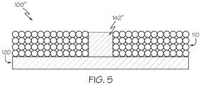
- the assembly 100 ′′ depicted in FIG. 5 another embodiment of the assembly 100 ′′ is schematically depicted. Similar to the embodiment described above and depicted in FIG. 4 , the assembly 100 ′′ includes the base substrate 120 and the plurality of sacrificial spheres 110 . Moreover, similar to the embodiment depicted in FIG. 4 , the assembly 100 ′′ depicted in FIG. 5 includes the solid channel 142 ′′ that is formed from a process other than fusing spheres of the plurality of sacrificial spheres 110 on the base substrate 120 . However, in the embodiment depicted in FIG. 5 , the solid channel 142 ′′ includes a rectangular cross-section and may be formed as a solid rectangular prism. While the embodiments depicted in FIGS.
- solid channels 142 ′ and 142 ′′ including a circular and a rectangular cross-section, respectively, it should be understood that these are merely examples, and solid channels according to embodiments described herein may include any suitably shaped cross-section to form the flow channel 140 ( FIG. 1 ).
- a block diagram of a method for forming an assembly 100 is depicted.
- the plurality of sacrificial spheres 110 are positioned along the base substrate 120 .
- the region 114 of the plurality of sacrificial spheres 110 are heated above a melting point of the plurality of sacrificial spheres 110 to form the solid channel 142 .
- the material is electrodeposited between the plurality of sacrificial spheres 110 and around the solid channel 142 .
- the plurality of sacrificial spheres 110 and the solid channel 142 are removed to form the MIO structure 108 ( FIG. 1 ) and the flow channel 140 ( FIG. 1 ) extending through the MIO structure 108 .
- a block diagram of another method for forming an assembly is depicted.
- the plurality of sacrificial spheres 110 are positioned along the base substrate 120 .
- the solid channel 142 ′, 142 ′′ is positioned between spheres of the plurality of sacrificial spheres.
- the material is electrodeposited between the plurality of sacrificial spheres 110 and around the solid channel 142 ′, 142 ′′.
- the plurality of sacrificial spheres 110 and the solid channel 142 ′, 142 ′′ are removed to form the MIO structure 108 ( FIG. 1 ) and the flow channel 140 ( FIG. 1 ) extending through the MIO structure 108 .
- embodiments described herein are generally directed to assemblies for cooling a heat generating device.
- embodiments described herein are directed to cooling assemblies including a MIO structure.
- One or more flow channels are formed within the MIO structure, and cooling fluid may be passed through the one or more flow channels.
- the one or more flow channels can increase the amount of cooling fluid that may be passed through the MIO structure, thereby increasing the amount of heat that can be dissipated from the heat-generating device.
- the one or more flow channels may be utilized to direct the cooling fluid through the MIO structure, for example to impinge the cooling fluid on a target surface to cool the heat-generating device.
Abstract
Description
Claims (19)
Priority Applications (1)
| Application Number | Priority Date | Filing Date | Title |
|---|---|---|---|
| US16/776,813 US11220426B2 (en) | 2020-01-30 | 2020-01-30 | Methods for forming flow channels in metal inverse opal structures |
Applications Claiming Priority (1)
| Application Number | Priority Date | Filing Date | Title |
|---|---|---|---|
| US16/776,813 US11220426B2 (en) | 2020-01-30 | 2020-01-30 | Methods for forming flow channels in metal inverse opal structures |
Publications (2)
| Publication Number | Publication Date |
|---|---|
| US20210238033A1 US20210238033A1 (en) | 2021-08-05 |
| US11220426B2 true US11220426B2 (en) | 2022-01-11 |
Family
ID=77410932
Family Applications (1)
| Application Number | Title | Priority Date | Filing Date |
|---|---|---|---|
| US16/776,813 Active US11220426B2 (en) | 2020-01-30 | 2020-01-30 | Methods for forming flow channels in metal inverse opal structures |
Country Status (1)
| Country | Link |
|---|---|
| US (1) | US11220426B2 (en) |
Citations (6)
| Publication number | Priority date | Publication date | Assignee | Title |
|---|---|---|---|---|
| WO2004099470A1 (en) | 2003-05-06 | 2004-11-18 | Fujitsu Limited | Porous alumina film and its forming method, magnetic recording medium, and magnetic storage device |
| US20080253411A1 (en) | 2004-04-16 | 2008-10-16 | D.K. And E.L. Mc Phail Enterprises Pty Ltd. | Optically Active Matrix with Void Structures |
| US20090174117A1 (en) * | 2006-04-12 | 2009-07-09 | Holger Winkler | Method for producing inverse opals having adjustable channel diameters |
| US8237538B2 (en) | 2007-04-09 | 2012-08-07 | The Board Of Trustees Of The University Of Illinois | Porous battery electrode for a rechargeable battery and method of making the electrode |
| US9559349B2 (en) * | 2011-07-29 | 2017-01-31 | The Board Of Trustees Of The University Of Illinois | Method of fabricating a three-dimensional (3D) porous electrode architecture for a microbattery |
| CN107478638A (en) | 2017-07-17 | 2017-12-15 | 中国科学院合肥物质科学研究院 | Individual layer counter opal structure of silver nano-grain assembling and its production and use |
-
2020
- 2020-01-30 US US16/776,813 patent/US11220426B2/en active Active
Patent Citations (7)
| Publication number | Priority date | Publication date | Assignee | Title |
|---|---|---|---|---|
| WO2004099470A1 (en) | 2003-05-06 | 2004-11-18 | Fujitsu Limited | Porous alumina film and its forming method, magnetic recording medium, and magnetic storage device |
| US20080253411A1 (en) | 2004-04-16 | 2008-10-16 | D.K. And E.L. Mc Phail Enterprises Pty Ltd. | Optically Active Matrix with Void Structures |
| EP1743209B1 (en) | 2004-04-16 | 2016-11-23 | D.K. And E.L. Mcphail Enterprises Pty Ltd | Method of forming an optically active matrix with void structures |
| US20090174117A1 (en) * | 2006-04-12 | 2009-07-09 | Holger Winkler | Method for producing inverse opals having adjustable channel diameters |
| US8237538B2 (en) | 2007-04-09 | 2012-08-07 | The Board Of Trustees Of The University Of Illinois | Porous battery electrode for a rechargeable battery and method of making the electrode |
| US9559349B2 (en) * | 2011-07-29 | 2017-01-31 | The Board Of Trustees Of The University Of Illinois | Method of fabricating a three-dimensional (3D) porous electrode architecture for a microbattery |
| CN107478638A (en) | 2017-07-17 | 2017-12-15 | 中国科学院合肥物质科学研究院 | Individual layer counter opal structure of silver nano-grain assembling and its production and use |
Also Published As
| Publication number | Publication date |
|---|---|
| US20210238033A1 (en) | 2021-08-05 |
Similar Documents
| Publication | Publication Date | Title |
|---|---|---|
| US9803938B2 (en) | Cooling assemblies having porous three dimensional surfaces | |
| CN108074890B (en) | Electronic assembly having a cooled chip layer with impingement channels and through-substrate vias | |
| EP2228821B1 (en) | Methods for Making Millichannel Substrate | |
| KR101706847B1 (en) | Semiconductor device with chip level heat dissipation using silicon | |
| TWI242865B (en) | Electro-osmotic pumps and micro-channels | |
| KR101695708B1 (en) | Semiconductor device and method of fabricating the same | |
| US9257365B2 (en) | Cooling assemblies and power electronics modules having multiple-porosity structures | |
| CN109789486B (en) | Optical or optoelectronic component and method for the production thereof | |
| Calame et al. | Experimental investigation of microchannel coolers for the high heat flux thermal management of GaN-on-SiC semiconductor devices | |
| US20100081191A1 (en) | Anisotropic heat spreader for use with a thermoelectric device | |
| US20200187392A1 (en) | Cooling devices including jet cooling with an intermediate mesh and methods for using the same | |
| US7288840B2 (en) | Structure for cooling a surface | |
| US9123697B2 (en) | Semiconductor cooling device | |
| JP6191660B2 (en) | Thermal conductor, semiconductor device provided with thermal conductor | |
| CN110192273A (en) | Method and apparatus for spreading high heat-flux in hot ground plane | |
| Guggenheim et al. | Roadmap review for cooling high-power GaN HEMT devices | |
| US11101193B2 (en) | Power electronics modules including integrated jet cooling | |
| US11220426B2 (en) | Methods for forming flow channels in metal inverse opal structures | |
| Daniel et al. | Enhanced cooling of electronic chips using combined diamond coating and microfluidics | |
| CN116546869A (en) | Novel micro-flow thermoelectric radiator, manufacturing method thereof and radiating method | |
| US11004769B2 (en) | Metal inverse opal substrate with integrated jet cooling in electronic modules | |
| JP6967654B2 (en) | Heat dissipation structure of semiconductor device and semiconductor device | |
| US7105382B2 (en) | Self-aligned electrodes contained within the trenches of an electroosmotic pump | |
| US10818576B2 (en) | Methods of forming power electronic assemblies using metal inverse opals and cap structures | |
| US20190237389A1 (en) | Cooling bond layer and power electronics assemblies incorporating the same |
Legal Events
| Date | Code | Title | Description |
|---|---|---|---|
| AS | Assignment |
Owner name: THE BOARD OF TRUSTEES OF THE UNIVERSITY OF ILLINOIS, ILLINOIS Free format text: ASSIGNMENT OF ASSIGNORS INTEREST;ASSIGNORS:BRAUN, PAUL;KOHANEK, JULIA;SINGHAL, GAURAV;SIGNING DATES FROM 20191211 TO 20200108;REEL/FRAME:051671/0128 Owner name: TOYOTA MOTOR ENGINEERING & MANUFACTURING NORTH AMERICA, INC., TEXAS Free format text: ASSIGNMENT OF ASSIGNORS INTEREST;ASSIGNOR:JOSHI, SHAILESH N.;REEL/FRAME:051671/0009 Effective date: 20200129 |
|
| FEPP | Fee payment procedure |
Free format text: ENTITY STATUS SET TO UNDISCOUNTED (ORIGINAL EVENT CODE: BIG.); ENTITY STATUS OF PATENT OWNER: LARGE ENTITY |
|
| STPP | Information on status: patent application and granting procedure in general |
Free format text: RESPONSE TO NON-FINAL OFFICE ACTION ENTERED AND FORWARDED TO EXAMINER |
|
| STPP | Information on status: patent application and granting procedure in general |
Free format text: NOTICE OF ALLOWANCE MAILED -- APPLICATION RECEIVED IN OFFICE OF PUBLICATIONS |
|
| STPP | Information on status: patent application and granting procedure in general |
Free format text: PUBLICATIONS -- ISSUE FEE PAYMENT RECEIVED |
|
| STPP | Information on status: patent application and granting procedure in general |
Free format text: PUBLICATIONS -- ISSUE FEE PAYMENT VERIFIED |
|
| STCF | Information on status: patent grant |
Free format text: PATENTED CASE |
|
| AS | Assignment |
Owner name: TOYOTA JIDOSHA KABUSHIKI KAISHA, JAPAN Free format text: ASSIGNMENT OF ASSIGNORS INTEREST;ASSIGNOR:TOYOTA MOTOR ENGINEERING & MANUFACTURING NORTH AMERICA, INC.;REEL/FRAME:058580/0220 Effective date: 20220107 |