US11218230B2 - Calibration system, antenna system and calibration method - Google Patents
Calibration system, antenna system and calibration method Download PDFInfo
- Publication number
- US11218230B2 US11218230B2 US17/252,686 US201917252686A US11218230B2 US 11218230 B2 US11218230 B2 US 11218230B2 US 201917252686 A US201917252686 A US 201917252686A US 11218230 B2 US11218230 B2 US 11218230B2
- Authority
- US
- United States
- Prior art keywords
- calibration
- transceivers
- signals
- transceiver
- signal
- Prior art date
- Legal status (The legal status is an assumption and is not a legal conclusion. Google has not performed a legal analysis and makes no representation as to the accuracy of the status listed.)
- Active
Links
Images


Classifications
-
- H—ELECTRICITY
- H04—ELECTRIC COMMUNICATION TECHNIQUE
- H04B—TRANSMISSION
- H04B17/00—Monitoring; Testing
- H04B17/10—Monitoring; Testing of transmitters
- H04B17/15—Performance testing
- H04B17/18—Monitoring during normal operation
-
- H—ELECTRICITY
- H04—ELECTRIC COMMUNICATION TECHNIQUE
- H04B—TRANSMISSION
- H04B17/00—Monitoring; Testing
- H04B17/10—Monitoring; Testing of transmitters
- H04B17/11—Monitoring; Testing of transmitters for calibration
- H04B17/12—Monitoring; Testing of transmitters for calibration of transmit antennas, e.g. of the amplitude or phase
Definitions
- the invention relates to a calibration system. Further, the present invention relates to an antenna system and to a calibration method.
- wireless communication networks are widely used for providing voice and data communication to users.
- Such wireless communication networks like e.g. LTE based or so called 4G networks, usually comprise a core network and a so called radio access network or RAN. It is understood, that each of these interrelated networks may comprise a plurality of different elements, modules or units that together provide the required communication capabilities.
- eNodeBs As part of the RAN so called eNodeBs or base stations provide the link between the operators network and the users mobile devices or user equipments (UEs). Usually the eNodeBs will comprise antennas that serve for transmitting outgoing signals to the UEs and for receiving incoming signals from the UEs. Up to now, most commonly passive or active antennas with fixed radiation patterns are used.
- Such conventional antennas may be replaced by massive MIMO antennas (antennas with a plurality of single antenna elements that may form and steer a plurality of beams at the same time).
- massive MIMO antennas a single transceiver, e.g. a combination of a transmitter and a receiver, is usually required for every antenna element.
- a calibration system for calibrating a number, i.e. one or more, of transceivers, each comprising an in-phase signal path and a quadrature signal path in receive direction and/or in transmit direction, the calibration system comprising a calibration signal generator that is configured to generate a predefined calibration signal for every one of the transceivers, a calibration transceiver that is coupled to the calibration signal generator and to the transceivers and that is configured supply the generated calibration signals each to the respective transceiver during operation of the transceivers, and/or that is configured to receive the predefined calibration signals each from one of the transceivers during operation of the transceivers, and a calibration unit that is configured to calibrate the in-phase signal paths and the quadrature signal paths of the transceivers during operation of the transceivers based on the calibration signals as they are received by the transceivers or based on the calibration signals as they are received by the calibration transceiver.
- An antenna system comprising a plurality of antenna elements, a transceiver for every one of the antenna elements that is coupled to the respective antenna element, and a calibration system according to the present invention.
- a calibration method for calibrating a number of transceivers, each comprising an in-phase signal path and a quadrature signal path in receive direction and/or in transmit direction comprising generating a predefined calibration signal for every one of the transceivers, supplying the generated calibration signals each to the respective transceiver during operation of the transceivers via a calibration transceiver or receiving the predefined calibration signals each from the respective one of the transceivers during operation of the transceivers in the calibration transceiver, and calibrating the in-phase signal paths and the quadrature signal paths of the transceivers during operation of the transceivers based on the calibration signals as they are received by the transceivers or based on the calibration signals as they are received by the calibration transceiver.
- the present invention is based on the finding that the direct-conversion transceivers used in modern massive MIMO antennas may comprise a plurality of different digital and/or analog signal processing elements that may comprise tolerances and temperature dependent characteristics. Further, such direct-conversion transceivers usually do not comprise built in calibration or compensation mechanisms, which allow the calibration while the transceiver is actively used for data transmission at the same time.
- transceiver may refer to any type of device that comprises a transmitter and/or a receiver for RF signals. Such devices may especially comprise a digital IQ-interface.
- An exemplary direct-conversion transceiver may consist of a receiver and a transmitter.
- the transceiver may also contain the analog-to-digital converters (ADCs) and digital-to-analog converters (DACs) to provide a digital interface towards a baseband processor, e.g. an IQ-interface.
- the baseband processor may therefore provide an in-phase signal (I-signal) and a quadrature signal (Q-signal) to the transmitter.
- the transmitter After converting the digital IQ-signals to analog signal, the transmitter first low-pass filters the analog signals to filter out aliases that come out of DACs. Then, the in-phase component is multiplied by a sinusoidal waveform that comes from a local transmitter RF oscillator.
- the analog Q-signal is multiplied by a 90 degree shifted version of the sinusoidal waveform.
- the multiplied in-phase and quadrature components are then added to form the RF transmit signal.
- This signal may then be provided e.g. via an amplifier and a RF output to an antenna element.
- the RF receiver may work in a similar but reverse order fashion.
- a direct-conversion transceiver may e.g. employ a low noise amplifier (LNA) at the first input stage of the receiver.
- the LNA amplifies the RF signal presented by an antenna element at the input of the receiver.
- the amplified signal is split into two identical signals.
- the first split signal is multiplied by a sinusoidal waveform that comes from a local receiver RF oscillator (RX LO).
- the multiplied signal is the so-called in-phase component (I-component) of the received signal.
- the second split signal is multiplied by a 90 degree shifted version of the sinusoidal waveform to form the quadrature component (Q-component) of the received signal.
- Both, in-phase and quadrature components are low pass filtered to filter out any unwanted components of the received signal to avoid distortion through aliasing when sampling the signal.
- the filtered in-phase and quadrature components are sampled and analog-to-digital converted to form the digital baseband signal, i.e. the received I-signal and Q-signal.
- the signal paths for the in-phase component and the quadrature components can slightly differ in gain. They also may exhibit a slightly different transfer function. Whereas the difference of the transfer function in the in-phase and quadrature components is not significant and can often be neglected, the gain difference is an important factor.
- the gain difference is also referred to as amplitude mismatch.
- the phase shift between the mixing waveforms may deviate from the exact 90 degrees causing the in-phase and quadrature component to be not 100% orthogonal. This impairment is typically referred to as phase imbalance. Amplitude mismatch and phase imbalance are both nonlinear effects that degrade the performance of a modem in both transmit and receive directions. Both imbalances together are often referred to as IQ imbalances.
- IQ imbalances As a result of IQ imbalances, the spectrum on the upper side of the carrier interferes with the spectrum on the lower side of the carrier and vice versa. In case the low-pass signal is single sided, IQ imbalances cause an image on the opposite side of the carrier. For OFDM, IQ imbalances introduce inter-carrier interference from the mirroring sub-carrier
- the present invention provides the calibration system that helps minimizing the IQ imbalances. It is understood, that although the calibration system is described in combination with transceivers, it may also be used with dedicated transmitters and receivers.
- the calibration system comprises the calibration signal generator that generates calibration signals for the single transceivers.
- the calibration signals will be provided to the transceivers during normal operation of the transceivers. Therefore, the calibration signal generator may generate calibration signals that do not interfere with the operational signals in the transceivers. This may e.g. be achieved by selecting respective signal frequencies or by providing the calibration signals with a signal amplitude or level that is below the noise level in the transceiver system. How such signals may be used for calibration of the transceivers will be explained in detail below.
- the calibration signal generator may generate a dedicated calibration signal for every transceiver. This may allow parallel testing of a plurality of transceivers. However, it is also possible for the calibration signal generator to generate the same calibration signal for the transceivers. This allows sequentially testing the single transceivers.
- the calibration signal may be provided to the transmitter or the receiver of the respective transceiver. If the signal is provided to the receiver of the transceiver, the calibration transceiver may emit the respective calibration signal to the respective transceiver. If the signal is provided to the transmitter of the transceiver, the calibration receiver may receive the calibration signal from the transceiver. In this case, the calibration signal generator may be coupled to the input side of the transmitter of the transceiver or to any element in the signal chain of the transmitter that may serve to couple in the calibration signal.
- transceivers usually do not comprise an RF loopback, an external loop and a calibration transceiver dedicated to calibration are provided by the present invention.
- a transceiver may have the option for an RF loopback which is an alternate path. However, this usually means that the output of that transceiver is switched off.
- the calibration transceiver may be provided free of IQ imbalances. Because the calibration transceiver may be switched into a loopback mode (either on chip or externally), a conventional calibration signal such as a single tone calibration scheme may be used for measurement and calibration of the calibration transmitter, e.g. periodically. An image rejection ratio of over 50 dB can be achieved by using the single tone scheme.
- the calibration unit may therefore analyze either the calibration signals as they are received by the respective transceivers from the calibration transceiver or the calibration signals as they are received by the calibration transceiver from the respective transceivers.
- the calibration unit may comprise respective signal processing elements, like e.g. filters, correlators or the like, that allow the calibration unit to process the calibration signals in the total signals provided by the respective transceivers or by the calibration transceiver, i.e. the calibration signals plus the operational signals received by the respective transceivers.
- respective signal processing elements like e.g. filters, correlators or the like, that allow the calibration unit to process the calibration signals in the total signals provided by the respective transceivers or by the calibration transceiver, i.e. the calibration signals plus the operational signals received by the respective transceivers.
- the calibration unit may e.g. receive the I-signal and the Q-signal from the respective transceiver. In contrast, if the transmitter of the transceiver is tested, the calibration unit may e.g. receive the I-signal and the Q-signal from the calibration transceiver.
- the calibration unit may e.g. compare the original calibration signal and the calibration signal as it is provided in the respective I- and Q-signals and determine the necessary calibration.
- the IQ imbalance phenomenon is mainly caused by none ⁇ 90° phase shifts and amplitude mismatches between the I- and the Q-signal path of the respective transmitter or receiver.
- the calibration unit may therefore determine the required adaption of the amplitudes and a required phase-shift in in the respective I- and Q-signal paths.
- the calibration unit may e.g. compensate the IQ imbalance using dedicated blocks, like e.g. a gain corrector (e.g. an amplifier or attenuator) and a phase shifter. These blocks may e.g. be placed in the in-phase and the quadrature signal paths accordingly.
- the calibration unit may also use a digital pre-compensation of the digital IQ signals in the base band processor.
- a digital phase shift may e.g. be performed by modifying the timing between the I-signal and Q-signal, i.e. by delaying either one of the I-signal and the Q-signal.
- the present invention allows using simple direct-conversion transceivers or respective transmitters and receivers in massive MIMO antennas.
- massive MIMO antennas may be calibrated with the help of the present invention without shutting down the antenna or interrupting the operation of the antenna for calibration.
- each calibration signal may comprise two orthogonal signals or two quasi-orthogonal signals.
- the calibration signals may e.g. be provided as complex calibration signals comprising two signals.
- One signal may form the real part of the complex calibration signal and the other signal may form the complex part of the calibration signal.
- the real part may refer to the I-signal and the complex part to the Q-signal.
- pl[n] may refer to the I-signal in the respective receiver or transmitter.
- the pQ[n] signal may be a signal that refers to the Q-signal in the respective receiver or transmitter.
- the pl[n] signal and the pQ[n] signals may be orthogonal or quasi-orthogonal signals.
- the index value [n] indicates that the signals may be provided as discrete series of signal values.
- orthogonal signals are mutually independent. This means that orthogonal signals may be transmitted simultaneously and may still be separated on the receiving side. Therefore, by using orthogonal signals for the calibration signals, it is possible to provide signals to the signal path that processes the I-signal and the signal path that processes the Q-signal at the same time.
- the orthogonal signals may be distinguished from each other by a unique signature.
- the unique signature may e.g. comprise:
- a signature may in general be any property of the signals that allows distinguishing a signal from other signals.
- a signature can e.g. be anything starting from a modulated binary sequence that is distinguished through the different binary sequences to signals that are unique with respect to their time or spectral characteristics.
- each calibration signal may comprises two pseudo noise signals, also called PN-sequences or PN-signals, especially band-limited pseudo noise signals, and more especially modulated pseudo-random binary sequences, also called PRBS.
- PRBS pseudo noise signals
- a special type pf PRBS that may be used is the so called Gold code, named after Robert Gold.
- the calibration signals may be provided as complex calibration signals comprising a pseudo noise signal that forms the real part of the complex calibration system and a pseudo noise signal that forms the complex part of the calibration signal.
- the real part pseudo noise signal refers to the I-signal and the complex part pseudo noise signal refers to the Q-signal.
- the calibration signal generator may generate the PN-sequences.
- the PN-sequences may be IQ modulated and filtered to the bandwidth of the operational signal.
- the resulting signal may then be provided to the respective transceiver from the calibration transceiver.
- the received calibration signal will be impaired by noise but also, in operational state, by the operational signal (e.g. LTE signals that will be superimposed with the calibration signal in practice.).
- PN-sequences allows introducing the PN-sequences into the operational signal of the transceivers with a signal level that is below the noise level in the respective system. Therefore, the operation of the system will not be influenced by the presence of the PN-sequences based calibration signals.
- the evaluation of the calibration signals may then e.g. be performed using correlators as will be described in further detail below.
- the calibration signals may comprise equal autocorrelation and zero cross-correlation.
- phase and amplitude imbalance in reception direction (RX) for a transceiver may be mathematically modelled as:
- ⁇ R cos( ⁇ R ) ⁇ j ⁇ R sin( ⁇ R ) (2)
- ⁇ R ⁇ R COS( ⁇ R )+ j sin( ⁇ R ) (3)
- X RF is the incoming RF signal
- X LO is the signal generated by the local oscillator
- Equation (1) the effect of IQ imbalance on the low pass signal is derived.
- the signal X L is distorted with a scaled version of its complex conjugate. Because of the complex conjugation, the spectrum on the upper side of the carrier interferes with the spectrum on the lower side of the carrier and vice versa. Thus, if the low-pass signal is single sided, IQ imbalance causes an image on the opposite side of the carrier.
- the interference is limited to mutual interference of two mirroring sub-carriers and the relative amount of interference is easily found.
- phase and amplitude imbalance in transmission direction (TX) for a transceiver may be mathematically modelled analogously.
- the present invention may measure the IQ imbalance of a transceiver as will be described below.
- PN-sequence that serve for the determination of IQ-imbalances according to the present invention have to fulfill certain requirements.
- Corresponding PN-sequences may e.g. be searched for in advance, e.g. by a trial and error method.
- the resulting PN-sequences may then e.g. be stored as the initial states in e.g. a memory of the calibration signal generator.
- the PN-sequences may comprise any length required and different sequences for the same length may also be stored.
- band limited PN sequences would be transmitted at different frequency offsets to the carrier.
- the band limitation would be less than the coherence bandwidth of the variation and multiple such measurements would be taken across the full bandwidth at various frequency offsets to sample the transfer function.
- the calibration unit may comprise a non-volatile memory. Measured IQ imbalance values may be stored in this non-volatile memory to improve the default values after system startup and to obtain information on the impact of system aging.
- the calibration system may comprise a coupling element for every transceiver configured to couple in a signal into the respective transceiver and/or couple out a signal out of the respective transceiver.
- the coupling elements may either be arranged outside of the transceivers, e.g. between the respective transceiver and the corresponding antenna element or inside of the transceiver. It is further understood, that instead of a single bidirectional coupling element in each case two unidirectional coupling elements may be used, one for coupling in a signal into the respective transceiver and one for coupling out a signal from the transceiver.
- Coupling elements in this regard may e.g. comprise directional couplers.
- Such directional couplers may e.g. be implemented as coupling lines or traces in a circuit of the transceivers or the respective antenna.
- the calibration unit may comprise a number, i.e. one or more, of correlators, also called correlator banks, that are each configured to correlate signals received by a specific one of the transceivers with the respective predetermined calibration signal and/or that are each configured to correlate signals received by the calibration transceiver with the respective predetermined calibration signal, wherein the calibration unit may be configured to calibrate the respective in-phase signal paths and the quadrature signal paths of the transceivers based on the correlation result.
- correlators also called correlator banks
- correlation may be used to analyze the differences between the original calibration signal and the calibration signal after being processed by a transceiver in order to determine the IQ imbalances of the transceiver.
- the correlation value for the PN sequence x[n] can be calculated as:
- x[n] and xQ[n] are Gold codes that have equal autocorrelation and zeros cross-correlation, hence, the correlation value rx,x* will be zero,
- the correlation value can be written as
- the received calibration signal will be impaired by noise but also, in operational state, by the operational signal (e.g. LTE signals that will be superimposed with the calibration signal in practice.).
- the operational signal e.g. LTE signals that will be superimposed with the calibration signal in practice.
- the SNR (signal to noise ration) of the correlation result is, therefore, quite low.
- the length of the PN sequences may therefore be chosen as long as required to achieve the target SNRs required for IQ imbalance compensation.
- the length of the PN sequence may also need to be adjusted to the present SNR.
- One solution is the consecutive use of multiple short sequences and to run an iterative calibration algorithm for the estimation of the IQ imbalance.
- the requirement for the image rejection may e.g. be 43 dB, thus, in this case the SNR of the correlation result has to be larger than 40 dB (e.g. 50 dB).
- the length of the used PN sequence has to be adapted accordingly, e.g. because the transmit power of the calibration signal is fixed.
- the level of the calibration signal may e.g. be 35 dB below the LTE signal in order not to impact the EVM (error vector magnitude).
- the calibration signal may be added to only one out of the eight transmit or receive paths, respectively, the calibration signal on that path is allowed to be eight times higher (9 dB).
- the calibration unit may be configured to determine the imbalances, especially regarding phase and amplitude, between the in-phase signal path and the quadrature signal path in receive direction and/or in transmit direction of a respective transceiver based on a least square regression algorithm.
- the measured/estimated correlation value directly relates to amplitude and phase imbalance values ⁇ R and ⁇ R , see equation (13). These values can be used as parameters for the transceiver to calibrate the IQ imbalance.
- the slope ⁇ is constant and can be obtained in advanced.
- the estimate of the phase correction value to compensates the phase imbalance is given as
- z ⁇ 0 z - ⁇ ⁇ ⁇ ⁇ _ . ( 20 )
- the calibration unit may be configured to tune parameters of elements in the in-phase signal paths and the quadrature signal paths of the transceivers.
- the calibration unit may be configured to perform a digital calibration of the in-phase signal paths and the quadrature signal paths of the transceivers by adapting the input signals to the transceivers accordingly and/or by adapting the output signals of the transceivers accordingly.
- the calibration unit may perform any of the two possibilities or a combination of the two possibilities of tuning parameters of the elements in the transceiver, i.e. adapt the hardware, and performing digital calculations with signals that are provided to the transceiver or that are received from the transceiver.
- the transceivers are required to comprise elements with a configuration interface.
- a configuration interface may be an analog interface, e.g. for tuning a phase shifter with a voltage or current, or may be a digital interface, e.g. for adapting DACs or ADCs or the like. It is understood, that additional or dedicated elements may be provided in the in-phase signal paths and the quadrature signal paths of the transceivers for tuning the amplitude and the phase of the respective signals.
- the calibration unit may in addition use a digital calibration that is performed on the IQ signals that are provided to or received from the transceivers.
- a pure digital IQ imbalance calibration may also be used in systems, where the transceivers do not comprise any tunable elements.
- the calibration system may serve for calibrating at least two transceivers, wherein the calibration transceiver may be embodied as one of the transceivers.
- Using one of the transceivers as calibration transceiver is especially beneficial in TDD (Time Domain Duplex) systems, where either the receivers or the transmitters are active at any point in time. Therefore, for calibrating the receivers, the transmitter of one of the transceivers may be used. Accordingly, for calibrating the transmitters, the receiver of one of the transceivers may be used.
- the calibration transceiver should be free of IQ imbalances and must therefore be calibrated. However, if the calibration transceiver is one of the transceivers, it is difficult to calibrate the calibration transceiver without interrupting normal operation of e.g. an antenna that comprises the transceivers.
- the calibration system may comprise a calibration transceiver calibration unit, which may be integrated into the calibration unit in one embodiment.
- the calibration transceiver calibration unit may e.g. calibrate the calibration transceiver by calculating the IQ imbalances for all other transceivers and taking the average IQ imbalance as the IQ imbalance of the calibration transceiver.
- the transmitter or the receiver of the calibration transceiver may be separated from the respective antenna and may be calibrated e.g. using a single tone scheme.
- the calibration transceiver may be periodically separated from the respective antenna or antenna element and may be calibrated with the single tone scheme. Especially in massive MIMO antennas with multiple transceivers the temporary loss of one of the transceivers and the corresponding temporary loss of signal quality may be small and acceptable.
- the calibration transceiver calibration unit may e.g. analyze the load situation of the antenna and only calibrate the calibration transceiver if it is not needed, e.g. the other transceivers are sufficient to operate the antenna in the respective load scenario with a predetermined performance.
- FIG. 1 shows a block diagram of an embodiment of a calibration system according to the present invention
- FIG. 2 shows a block diagram of an embodiment of an antenna system according to the present invention
- FIG. 3 shows a block diagram of an embodiment of a transceiver for use in an embodiment of an antenna system according to the present invention
- FIG. 4 shows a block diagram of another embodiment of a transceiver for use in an embodiment of an antenna system according to the present invention
- FIG. 5 shows a block diagram of another embodiment of an antenna system according to the present invention.
- FIG. 6 shows a flow diagram of an embodiment of a calibration method according to the present invention.
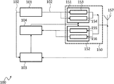
- FIG. 1 shows a block diagram of a calibration system 100 .
- the calibration system 100 serves for calibrating a number of transceivers 150 , of which only one is shown for sake of simplicity.
- the transceiver 150 comprises a transmitter 151 with an in-phase signal path 153 and a quadrature signal path 154 in receive direction, and a receiver 152 with an in-phase signal path 155 and a quadrature signal path 156 in transmit direction.
- the transmitter 151 and the receiver 152 are both coupled to an antenna element 157 .
- the calibration system 100 comprises a calibration signal generator 101 that is coupled to the transceiver 150 and to a calibration transceiver 103 .
- the calibration transceiver 103 and the receiver 152 are coupled to a calibration unit 104 on the input side.
- the calibration unit 104 is further coupled on its output side to the transmitter 151 and the receiver 152 .
- the calibration signal generator 101 generates a predefined calibration signal 102 for calibrating the transceiver 150 .
- the calibration signal 102 may be provided to the transceiver 150 , i.e. the transmitter 151 , directly from the signal generator 101 .
- the calibration signal 102 may be provided to the transceiver 150 , i.e. the receiver 152 , via the calibration transceiver 103 .
- the calibration transceiver 103 in order to calibrate the receiver 152 may therefore supply the generated calibration signal 102 to the transceiver 150 during operation of the transceiver 150 in the form of RF signals that may then be coupled into the receiving signal path of the antenna element 157 and the transceiver 150 .
- the receiver 152 will then supply IQ-signals, i.e. an I-signal and a Q-signal, to the calibration unit 104 . It is understood, that also not shown the IQ-signals may also be provided to a baseband processor for further processing of the operational signals that are included in the output IQ-signals of the receiver 152 .
- the signal generator 101 transmits the calibration signal 102 to the transmitter 151 that generates a respective RF signal.
- the calibration transceiver 103 will therefore receive the calibration signal 102 together with the operational signals from one of the transceivers 150 during operation of the transceiver 150 . It is understood, that some kind of mixing of the IQ signals of the baseband processor and the calibration signal 102 may be performed, e.g. by adding the calibration signal 102 to the operational IQ signals, e.g. in the baseband processor or a dedicated adder.
- the calibration unit 104 calibrates the in-phase signal paths 153 , 155 and the quadrature signal paths 154 , 156 of the transceiver 150 during operation of the transceiver 150 based on the calibration signals 102 after they traveled through the transmitter 151 or the receiver 152 of the transceiver 150 .
- the calibration system 100 may be used with any number of transceivers.
- the transceivers may then e.g. be calibrated sequentially at predetermined intervals.
- more than one calibration transceiver 103 may be provided in the calibration system 100 . In this case more than one of the transceivers may be calibrated simultaneously.
- orthogonal calibration signals 102 may be used, that because of their orthogonality may be separated in the receiver, i.e. the calibration transceiver 103 .
- FIG. 2 shows a block diagram of an antenna system 210 .
- the antenna system 210 comprises a baseband processor 211 that is coupled to a signal processing unit 212 .
- the signal processing unit 212 is coupled to a plurality of transceivers 250 , 260 , 261 . It is understood, that although three transceivers 250 , 260 , 261 are shown, any number of transceivers may be provided (indicated by three dots).
- the transceivers 250 , 260 , 261 are each further coupled to a respective antenna element 257 , 258 , 259 for transmitting and receiving RF signals.
- the antenna system 210 further comprises a calibration transceiver 203 that is coupled via a switch 215 and coupling lines 216 , 217 , 218 to the signal paths between the antenna elements 257 , 258 , 259 and the transceivers 250 , 260 , 261 .
- the calibration transceiver 203 is further coupled to the calibration blocks 214 .
- a local reference clock 219 is provided that is coupled to the calibration transceiver 203 , the transceivers 250 , 260 , 261 , and a clock synchronization unit 220 of the signal processing unit 212 .
- the signal processing unit 212 comprises beamforming blocks 213 and calibration blocks 214 .
- the beamforming blocks 213 may e.g. comprise beamforming functions in transmit and in receive direction.
- the calibration blocks 213 may e.g. comprise at least part of the calibration unit of the present invention.
- the calibration blocks 213 may comprise calibration functions that perform a calibration of the output level and phase between the different transceivers 250 , 260 , 261 (i.e. an inter-transceiver calibration—as opposed to the intra-transceiver calibration of the present invention)
- the calibration transceiver 203 may be sequentially coupled to the single transceivers 250 , 260 , 261 by controlling the switch 215 accordingly.
- the coupling lines 216 , 217 , 218 allow the calibration transceiver 203 to provide the calibration signal in RF form to the respective transceiver 250 , 260 , 261 .
- the calibration signal may be provided from the respective calibration blocks 214 in the signal processing unit 212 to the respective transceivers 250 , 260 , 261 as IQ signals.
- the calibration transceiver 203 may then receive RF signals, which include the calibration signals, from the respective transceiver 250 , 260 , 261 .
- the further signal processing and determination of the IQ imbalance of the respective transceivers 250 , 260 , 261 may then be performed in the signal processing unit 212 , e.g. in respective calibration blocks 214 .
- the calibration transceiver 203 may be pre-calibrated prior to performing the calibration of the transceivers 250 , 260 , 261 .
- the calibration transceiver 203 may e.g. be calibrated using a single tone calibration scheme, while it is not connected to any of the transceivers 250 , 260 , 261 .
- FIG. 2 shows an antenna system 210 that may e.g. be used in FDD and TDD systems. However, if the antenna system 210 is used in a TDD system, the antenna system 210 may either transmit RF signals or receive RF signals at any point in time. Therefore, either the transmitters or the receivers of the transceivers 250 , 260 , 261 will be unused at any point in time. It is therefore possible to use one of the transceivers 250 , 260 , 261 as calibration transceiver 203 .
- the receiver of the transceiver 250 , 260 , 261 that serves as calibration transceiver 203 may receive the calibration signals from the transceiver 250 , 260 , 261 that is to be calibrated, i.e. the respective transmitter. While the antenna system 210 is receiving RF signals, the transmitter of the transceiver 250 , 260 , 261 that serves as calibration transceiver 203 may provide the calibration signals as RF signals to the respective transceiver 250 , 260 , 261 that is to be calibrated, i.e. the respective receiver.
- FIG. 3 shows a detailed block diagram of a transceiver 350 that may e.g. be used in the antenna system 210 of FIG. 2 .
- the transceiver 350 comprises a transceiver IC 327 that may receive an IQ-signal or provide an IQ-signal, e.g. to a baseband processor.
- the transceiver IC 327 is coupled to a duplexer 328 via a bandpass filter 335 and a low noise amplifier 334 in the receive signal path and via a bandpass filter 336 and a power amplifier 337 in the transmit path.
- the duplexer 328 comprises a RX duplex filter 329 in the receive path and a TC duplex filter 330 in the transmit path.
- the RX duplex filter 329 and the TC duplex filter 330 are both coupled to a diplexer 331 that provides a RF signal 332 or receives an RF signal 332 .
- the transceiver 350 further comprises coupling element 302 and coupling element 333 .
- the coupling element 302 is coupled to the receive signal path between the duplexer 328 and the low noise amplifier 334 .
- the coupling element 333 is coupled between the power amplifier 337 and the duplexer 328 in the transmit signal path.
- the coupling elements 302 , 333 may be used as alternative to the arrangement of FIG. 2 to couple in signals into and couple out signals out of the transceiver IC 327 .
- FIG. 4 shows a block diagram of another a transceiver 450 .
- the transceiver 450 is a direct conversion transceiver 450 that comprises a transmitter 451 and a receiver 452 .
- An exemplary arrangement is described in detail for the transmitter 451 .
- the receiver 452 comprises analogous elements for receiving RF signals.
- the transmitter 451 comprises a digital IQ interface comprising a DAC 470 for the I-signal and a DAC 471 for the Q-signal.
- a low pass filter 472 is coupled to the DAC 470 and a low pass filter 473 is coupled to the DAC 471 .
- a local oscillator 477 provides a sinusoidal waveform that is mixed by mixer 474 with the output of low pass filter 472 .
- the sinusoidal waveform is further phase-shifted by phase-shifter 475 by 900 and mixed by mixer 476 with the output of low pass filter 473 .
- the output signals of mixer 474 and mixer 476 are added together by adder 478 .
- the output of adder 478 is amplifier by amplifier 479 and output as RF signal 480 .
- a plurality of elements may comprise tolerances.
- DACs 470 , 471 , low pass filters 472 , 473 and mixers 474 may comprise amplitude tolerances.
- the phase-shifter 475 may shift the incoming signal by more or less than exactly 90°.
- these elements may be the source of IQ-imbalances in the transmitter 451 .
- the receiver 452 comprises a similar arrangement.
- the adder 478 is removed and instead of DACs 470 , 471 there are ADCs provided. However, these ADCs may comprise similar tolerances as the DACs 470 , 471 .
- these elements may be the source of IQ-imbalances in the transmitter 452 .
- FIG. 5 shows a block diagram of an antenna system 510 .
- the antenna system 510 comprises a digital domain 581 and an analog domain 582 . Bridging the digital domain 581 and the analog domain 582 three transceivers are shown, wherein only the first transceiver 550 is provided with a reference sign. It is understood, that any number of transceivers may be provided. In the following only the signal chain for transceiver 550 will be explained in detail. It is understood, that the signal chains of the other transceivers may be provided analogously. It is further understood, that only the signal chain corresponding to the calibration of the transceiver 550 is provided with reference signs. The signal chain for processing operational signals is omitted for sake of clarity.
- the digital output of transceiver 550 is coupled to a receive phase & time correction module 584 .
- the digital input of transceiver 550 is coupled to a transmit phase & time correction module 585 .
- the receive phase & time correction module 584 is coupled via a selection switch 592 and a direction switch 591 to a correlator bank 589 .
- the transmit phase & time correction module 585 is coupled via direction switch 590 and selection switch 593 to the calibration signal generator 501 .
- a calibration transceiver 503 is provided.
- the digital output of calibration transceiver 503 is coupled via a receive phase & time correction module 586 to direction switch 591 .
- the digital input of the transceiver 550 is coupled via transmit phase & time correction module 587 to the direction switch 590 .
- the direction switches 590 , 591 serve to select the direction of the calibration. They may be used to select if the calibration signal is transmitted to the transceiver 550 and received via calibration transceiver 503 , or if the calibration signal is transmitted to calibration transceiver 503 and received via transceiver 550 .
- a switching matrix 583 is further provided on the RF interface of the calibration transceiver 503 .
- the switching matrix 583 comprises five different switches that allow coupling the RF interface of the calibration transceiver 503 to transmitter 550 either in receive or transmit direction and that further allow coupling the calibration transceiver 503 Bitteumble Sie hier an, womit der calibration transceiver 503 kann oppeltluate (Signals: RXTX_CAL etc.).
- FIG. 6 shows a flow diagram of a calibration method for calibrating a number of transceivers 150 , 250 , 260 , 261 , 350 , 450 , 550 , each comprising an in-phase signal path 153 , 155 and a quadrature signal path 154 , 156 in receive direction and/or in transmit direction.
- the calibration method comprises generating S 1 a predefined calibration signal 102 , 302 , 333 for every one of the transceivers 150 , 250 , 260 , 261 , 350 , 450 , 550 .
- the calibration method comprises supplying S 2 a the generated calibration signals 102 , 302 , 333 each to the respective transceiver 150 , 250 , 260 , 261 , 350 , 450 , 550 during operation of the transceivers 150 , 250 , 260 , 261 , 350 , 450 , 550 via a calibration transceiver 103 , 203 , 503 , or receiving S 2 b the predefined calibration signals 102 , 302 , 333 each from the respective one of the transceivers 150 , 250 , 260 , 261 , 350 , 450 , 550 during operation of the transceivers 150 , 250 , 260 , 261 , 350 , 450 , 550 in the calibration transceiver 103 , 203 , 503 .
- the method also comprises calibrating S 3 the in-phase signal paths 153 , 155 and the quadrature signal paths 154 , 156 of the transceivers 150 , 250 , 260 , 261 , 350 , 450 , 550 during operation of the transceivers 150 , 250 , 260 , 261 , 350 , 450 , 550 based on the calibration signals 102 , 302 , 333 as they are received by the transceivers 150 , 250 , 260 , 261 , 350 , 450 , 550 or based on the calibration signals 102 , 302 , 333 as they are received by the calibration transceiver 103 , 203 , 503 .
- Supplying S 2 a or receiving S 2 b may comprise coupling in a signal into the respective transceiver 150 , 250 , 260 , 261 , 350 , 450 , 550 and/or coupling out a signal out of the respective transceiver 150 , 250 , 260 , 261 , 350 , 450 , 550 via a coupling element.
- a coupling element may be provided.
- Each one of the calibration signals 102 , 302 , 333 may for example comprises two orthogonal signals or two quasi-orthogonal signals.
- Each one of the calibration signals 102 , 302 , 333 may especially comprise two pseudo noise signals, especially band-limited pseudo noise signals, and more especially modulated pseudo-random binary sequences. Such signals may be emitted concurrently and may still be separated and processed separately at the receiver side.
- the calibration signals 102 , 302 , 333 may further comprise equal autocorrelation and zero cross-correlation.
- the calibration method may comprise correlating signals received by a specific one of the transceivers 150 , 250 , 260 , 261 , 350 , 450 , 550 with the respective predetermined calibration signal 102 , 302 , 333 and/or correlating signals received by the calibration transceiver 103 , 203 , 503 with the respective predetermined calibration signal 102 , 302 , 333 , wherein calibrating the respective in-phase signal paths 153 , 155 and the quadrature signal paths 154 , 156 of the transceivers 150 , 250 , 260 , 261 , 350 , 450 , 550 is performed based on the correlation result.
- the calibration method may comprise determining the imbalances between the in-phase signal path 153 , 155 and the quadrature signal path 154 , 156 in receive direction and/or in transmit direction of a respective transceiver 150 , 250 , 260 , 261 , 350 , 450 , 550 based on a least square regression algorithm.
- the step of calibrating S 3 may comprise tuning parameters of elements in the in-phase signal paths 153 , 155 and the quadrature signal paths 154 , 156 of the transceivers 150 , 250 , 260 , 261 , 350 , 450 , 550 .
- the step of calibrating S 3 may comprise performing a digital calibration of the in-phase signal paths 153 , 155 and the quadrature signal paths 154 , 156 of the transceivers 150 , 250 , 260 , 261 , 350 , 450 , 550 by adapting the input signals to the transceivers 150 , 250 , 260 , 261 , 350 , 450 , 550 accordingly and/or by adapting the output signals of the transceivers 150 , 250 , 260 , 261 , 350 , 450 , 550 accordingly.
- the calibration method may be used for calibrating at least two transceivers 150 , 250 , 260 , 261 , 350 , 450 , 550 .
- supplying S 2 a and receiving S 2 b may be performed with one of the transceivers 150 , 250 , 260 , 261 , 350 , 450 , 550 .
- the present invention provides a calibration system 100 for calibrating a number of transceivers 150 , 250 , 260 , 261 , 350 , 450 , 550 , each comprising an in-phase signal path 153 , 155 and a quadrature signal path 154 , 156 in receive direction and/or in transmit direction, the calibration system 100 comprising a calibration signal generator 101 , 501 that is configured to generate a predefined calibration signal 102 , 302 , 333 for every one of the transceivers 150 , 250 , 260 , 261 , 350 , 450 , 550 , a calibration transceiver 103 , 203 , 503 that is coupled to the calibration signal generator 101 , 501 and to the transceivers 150 , 250 , 260 , 261 , 350 , 450 , 550 and that is configured supply the generated calibration signals 102 , 302 , 333 each to the respective transceiver 150 , 250 , 260 , 261
Abstract
Description
-
- The period, when the signal is sent.
- The frequency on which the signal is sent,
- The PN-code in case the calibration signal uses pseudo-noise signals
- In a more generic sense: by its waveform
- In case of the PN-code: by its pseudo random binary sequence.
where:
αR=cos(ϕR)−jϵ R sin(ϕR) (2)
βR=ϵR COS(ϕR)+j sin(ϕR) (3)
Where XRF is the incoming RF signal, XLO is the signal generated by the local oscillator, εR refers to the amplitude error of the in-phase signal path and the quadrature signal path, ϕR refers to the phase error of the in-phase signal path and the quadrature signal path, Xi is the signal in the in-phase signal path, and XQ is the signal in the quadrature signal path.
-
- zero mean value (that is e.g. present in balanced Gold codes)
- equal auto-correlation
- zero cross-correlation with one another.
with x[n]=x[n]+jxQ[n]. In one embodiment, x[n] and xQ[n] are Gold codes that have equal autocorrelation and zeros cross-correlation, hence, the correlation value rx,x* will be zero,
{tilde over (y)}[n]=αR x I[n]+βR x Q[n] (7)
=cos(ϕR)(1+ϵR)x I[n]+j sin(ϕR)(1−ϵR)x I[n]+j cos(ϕR)(1−ϵR)x Q[n]+sin(ϕR)(1+ϵR)x Q[n] (8)
r x,
=2r x
r x,
r x,{tilde over (y)}*≈2r x
SNR r =SNR+3(N+1)dB (14)
z[n]=ψα[n]+z 0+ξ[n] (15)
where n is the iteration index, z[n]=Im{r[n]x,y
z=ψα+z 0 (16)
which is the “best” fit for the data point (measurements), understood as in the least-squares approach.
where
- 100 calibration system
- 101, 501 calibration signal generator
- 102, 302, 333 calibration signal
- 103, 203, 503 calibration transceiver
- 104 calibration unit
- 150, 250, 260, 261, 350, 450, 550 transceiver
- 151, 451 transmitter
- 152, 452 receiver
- 153, 155 in-phase signal path
- 154, 156 quadrature signal path
- 157, 257, 258, 259, 557 antenna element
- 210, 510 antenna system
- 211 baseband processor
- 212 signal processing unit
- 213 beamforming blocks
- 214 calibration blocks
- 215 switch
- 216, 217, 218 coupling element
- 219 local reference clock
- 220 clock synchronization
- 325 output signals
- 326 input signals
- 327 transceiver IC
- 328 duplexer
- 329 RX duplex filter
- 330 TX duplex filter
- 331 diplexer
- 332 RF signal
- 334 low noise amplifier
- 335, 336 band pass filter
- 337 power amplifier
- 470, 471 DAC
- 472, 473 low pass filter
- 474, 476 mixer
- 475 phase shifter
- 477 local oscillator
- 478 adder
- 479 amplifier
- 480 RF signal
- 581 digital domain
- 582 analog domain
- 583 switching matrix
- 584, 586 receive phase & time correction module
- 585, 587 transmit phase & time correction module
- 588 timer
- 589 correlator
- 590, 591, 592, 593 switch
- S1, S2 a, S2 b, S3 method steps
Claims (20)
Applications Claiming Priority (4)
| Application Number | Priority Date | Filing Date | Title |
|---|---|---|---|
| EP18178177.4 | 2018-06-18 | ||
| EP8178177 | 2018-06-18 | ||
| EP18178177.4A EP3584963B1 (en) | 2018-06-18 | 2018-06-18 | Calibration system and calibration method |
| PCT/EP2019/065384 WO2019243139A1 (en) | 2018-06-18 | 2019-06-12 | Calibration system, antenna system and calibration method |
Publications (2)
| Publication Number | Publication Date |
|---|---|
| US20210281335A1 US20210281335A1 (en) | 2021-09-09 |
| US11218230B2 true US11218230B2 (en) | 2022-01-04 |
Family
ID=62712791
Family Applications (1)
| Application Number | Title | Priority Date | Filing Date |
|---|---|---|---|
| US17/252,686 Active US11218230B2 (en) | 2018-06-18 | 2019-06-12 | Calibration system, antenna system and calibration method |
Country Status (3)
| Country | Link |
|---|---|
| US (1) | US11218230B2 (en) |
| EP (1) | EP3584963B1 (en) |
| WO (1) | WO2019243139A1 (en) |
Families Citing this family (3)
| Publication number | Priority date | Publication date | Assignee | Title |
|---|---|---|---|---|
| CN111541631B (en) * | 2020-04-10 | 2021-08-13 | 清华大学 | Channel estimation method and device based on IQ imbalance MIMO system |
| CN114665989A (en) * | 2020-12-22 | 2022-06-24 | 中兴通讯股份有限公司 | Antenna correction method, device and system |
| US20230216574A1 (en) * | 2022-01-04 | 2023-07-06 | Meta Platforms, Inc. | Systems and methods for massive multiple-input multiple-output antenna calibration |
Citations (17)
| Publication number | Priority date | Publication date | Assignee | Title |
|---|---|---|---|---|
| US5696485A (en) * | 1996-11-06 | 1997-12-09 | Ford Global Technologies, Inc. | Method for charging a transponder |
| US20050156662A1 (en) * | 2004-01-16 | 2005-07-21 | Arun Raghupathy | Amplifier predistortion and autocalibration method and apparatus |
| US7006824B1 (en) * | 2002-09-10 | 2006-02-28 | Marvell International Ltd. | Frame/packet-based calibration for wireless transceivers |
| US20070291883A1 (en) * | 2006-06-14 | 2007-12-20 | Jared Welz | Method and apparatus for I/Q imbalance compensation |
| US7463866B1 (en) * | 2005-04-13 | 2008-12-09 | Rf Micro Devices, Inc. | I/Q mismatch calibration of direct conversion transceivers using the OFDM short training sequence |
| EP2040333A1 (en) | 2007-09-24 | 2009-03-25 | Astrium GmbH | Method and device for calibrating an array antenna |
| US20090227214A1 (en) * | 2002-09-03 | 2009-09-10 | Theodore Georgantas | Method and system for calibrating a multi-mode, multi-standard transmitter and receiver |
| US7715836B2 (en) * | 2002-09-03 | 2010-05-11 | Broadcom Corporation | Direct-conversion transceiver enabling digital calibration |
| US20130210375A1 (en) * | 2012-02-14 | 2013-08-15 | Intel Mobile Communications GmbH | Cancellation of RF Second-Order Intermodulation Distortion |
| US20130260844A1 (en) | 2012-03-28 | 2013-10-03 | Andrew Llc | Series-connected couplers for active antenna systems |
| US20130336376A1 (en) * | 2012-06-14 | 2013-12-19 | Gary Lang Do | Systems for Calibration of Wireless Electronic Devices |
| US20150118970A1 (en) * | 2013-10-30 | 2015-04-30 | Samsung Electronics Co., Ltd. | Rf loopback via antenna coupling for calibration of multiple transceiver systems |
| US20160248468A1 (en) * | 2015-02-24 | 2016-08-25 | Infineon Technologies Ag | Communication device and method for calibrating an oscillator |
| US9621312B2 (en) * | 2012-11-26 | 2017-04-11 | Aviacomm Inc. | RF transceiver architecture for flexible configuration of RF resources |
| US20170358950A1 (en) * | 2016-06-10 | 2017-12-14 | Ossia Inc. | Wireless Power Transmission For Near And Far Field Applications |
| US20190007094A1 (en) * | 2017-06-30 | 2019-01-03 | Intel Corporation | Cable Modem Transceiver, Cable Modem, Cable Modem Communication System, Processor for a Cable Modem Transceiver, Method for Calibrating a Cable Modem Transceiver, and Computer Program |
| US20190200270A1 (en) * | 2016-09-28 | 2019-06-27 | Intel IP Corporation | Apparatuses and methods for measuring neighboring inter-frequency or inter-rat cells |
-
2018
- 2018-06-18 EP EP18178177.4A patent/EP3584963B1/en active Active
-
2019
- 2019-06-12 WO PCT/EP2019/065384 patent/WO2019243139A1/en active Application Filing
- 2019-06-12 US US17/252,686 patent/US11218230B2/en active Active
Patent Citations (17)
| Publication number | Priority date | Publication date | Assignee | Title |
|---|---|---|---|---|
| US5696485A (en) * | 1996-11-06 | 1997-12-09 | Ford Global Technologies, Inc. | Method for charging a transponder |
| US20090227214A1 (en) * | 2002-09-03 | 2009-09-10 | Theodore Georgantas | Method and system for calibrating a multi-mode, multi-standard transmitter and receiver |
| US7715836B2 (en) * | 2002-09-03 | 2010-05-11 | Broadcom Corporation | Direct-conversion transceiver enabling digital calibration |
| US7006824B1 (en) * | 2002-09-10 | 2006-02-28 | Marvell International Ltd. | Frame/packet-based calibration for wireless transceivers |
| US20050156662A1 (en) * | 2004-01-16 | 2005-07-21 | Arun Raghupathy | Amplifier predistortion and autocalibration method and apparatus |
| US7463866B1 (en) * | 2005-04-13 | 2008-12-09 | Rf Micro Devices, Inc. | I/Q mismatch calibration of direct conversion transceivers using the OFDM short training sequence |
| US20070291883A1 (en) * | 2006-06-14 | 2007-12-20 | Jared Welz | Method and apparatus for I/Q imbalance compensation |
| EP2040333A1 (en) | 2007-09-24 | 2009-03-25 | Astrium GmbH | Method and device for calibrating an array antenna |
| US20130210375A1 (en) * | 2012-02-14 | 2013-08-15 | Intel Mobile Communications GmbH | Cancellation of RF Second-Order Intermodulation Distortion |
| US20130260844A1 (en) | 2012-03-28 | 2013-10-03 | Andrew Llc | Series-connected couplers for active antenna systems |
| US20130336376A1 (en) * | 2012-06-14 | 2013-12-19 | Gary Lang Do | Systems for Calibration of Wireless Electronic Devices |
| US9621312B2 (en) * | 2012-11-26 | 2017-04-11 | Aviacomm Inc. | RF transceiver architecture for flexible configuration of RF resources |
| US20150118970A1 (en) * | 2013-10-30 | 2015-04-30 | Samsung Electronics Co., Ltd. | Rf loopback via antenna coupling for calibration of multiple transceiver systems |
| US20160248468A1 (en) * | 2015-02-24 | 2016-08-25 | Infineon Technologies Ag | Communication device and method for calibrating an oscillator |
| US20170358950A1 (en) * | 2016-06-10 | 2017-12-14 | Ossia Inc. | Wireless Power Transmission For Near And Far Field Applications |
| US20190200270A1 (en) * | 2016-09-28 | 2019-06-27 | Intel IP Corporation | Apparatuses and methods for measuring neighboring inter-frequency or inter-rat cells |
| US20190007094A1 (en) * | 2017-06-30 | 2019-01-03 | Intel Corporation | Cable Modem Transceiver, Cable Modem, Cable Modem Communication System, Processor for a Cable Modem Transceiver, Method for Calibrating a Cable Modem Transceiver, and Computer Program |
Non-Patent Citations (3)
| Title |
|---|
| International Search Report and Written Opinion for PCT/EP2019/065384 (11pages). |
| KLADOVSCIKOV LEONID; NAVICKAS ROMUALDAS: "Review of self tuning methods for direct conversion transceivers", 2017 OPEN CONFERENCE OF ELECTRICAL, ELECTRONIC AND INFORMATION SCIENCES (ESTREAM), IEEE, 27 April 2017 (2017-04-27), pages 1 - 6, XP033259680, DOI: 10.1109/eStream.2017.7950308 |
| Kladovscikov, Leonid etal, "Review of Self Tuning Methods for Direct Conversion Transceivers", 2017 Open Conference of Electrical, Electronic and Information Sciences (ESTREAM), IEEE, Apr. 27, 2017, pp. 1-6, XP033259680, DOI: 10.1109/ESTREAM.2017.7950308; abstract left-hand column—p. 3. |
Also Published As
| Publication number | Publication date |
|---|---|
| EP3584963B1 (en) | 2022-01-05 |
| US20210281335A1 (en) | 2021-09-09 |
| WO2019243139A9 (en) | 2020-02-13 |
| WO2019243139A1 (en) | 2019-12-26 |
| EP3584963A1 (en) | 2019-12-25 |
Similar Documents
| Publication | Publication Date | Title |
|---|---|---|
| US10794993B2 (en) | Method and apparatus for calibrating an IQ modulator | |
| US9509355B2 (en) | Calibration of quadrature imbalance via loopback phase shifts | |
| US9231715B2 (en) | I/Q mismatch compensation method and apparatus | |
| US8526518B2 (en) | Imbalance compensation for direct conversion communication systems | |
| US11218230B2 (en) | Calibration system, antenna system and calibration method | |
| US20160359614A1 (en) | Adaptive I/Q Mismatch Calibration | |
| US9344302B2 (en) | Loopback technique for IQ imbalance estimation for calibration in OFDM systems | |
| US7174146B2 (en) | Method and apparatus for I/Q mismatch calibration in a receiver | |
| US20110292978A1 (en) | Calibration of quadrature imbalances using wideband signals | |
| KR20070061917A (en) | Techniques for correcting for phase and amplitude offsets in a mino radio device | |
| Singh et al. | Millimeter-wave full duplex radios | |
| US8711904B2 (en) | Calibration method for non-ideal transceivers | |
| US7123896B2 (en) | Method and apparatus for I/Q mismatch calibration in a receiver | |
| US8526533B2 (en) | Systems and methods for measuring I-Q mismatch | |
| Mailand | System analysis of six-port-based RF-receivers | |
| JP2001526872A (en) | Calibration method for n-port receiver | |
| Askar et al. | Full-Duplex wireless transceiver in presence of I/Q mismatches: Experimentation and estimation algorithm | |
| US20070147484A1 (en) | Apparatus and method for signal matching in a communication system | |
| Inti | Time-varying frequency selective IQ imbalance estimation and compensation | |
| KR20230127115A (en) | ELECTRONIC DEVICE AND OPERATING METHOD TO COMPENSATE In-phase/Quadrature Imbalance | |
| Wiers | Mirror, Mirror on the Wall—Understanding Image Rejection and Its Impact on Desired Signals | |
| Tang et al. | Self-Synchronized DS/SS With High Spread Factors for Robust Millimeter-Wave Datalinks | |
| Manoliu et al. | Frequency and Phase Investigation of the Local Oscillator Offset in a W-Band Satellite Communication Link | |
| KR101078801B1 (en) | I/q calibration for walking-if architectures | |
| Olopade | Concurrent Dual Band Six Port Receiver |
Legal Events
| Date | Code | Title | Description |
|---|---|---|---|
| FEPP | Fee payment procedure |
Free format text: ENTITY STATUS SET TO UNDISCOUNTED (ORIGINAL EVENT CODE: BIG.); ENTITY STATUS OF PATENT OWNER: LARGE ENTITY |
|
| AS | Assignment |
Owner name: XILINX, INC., CALIFORNIA Free format text: ASSIGNMENT OF ASSIGNORS INTEREST;ASSIGNORS:GRIEGER, MICHAEL;POLLAKIS, ALEXANDROS;AUE, VOLKER;AND OTHERS;SIGNING DATES FROM 20201016 TO 20210107;REEL/FRAME:055024/0981 |
|
| STPP | Information on status: patent application and granting procedure in general |
Free format text: NOTICE OF ALLOWANCE MAILED -- APPLICATION RECEIVED IN OFFICE OF PUBLICATIONS |
|
| STPP | Information on status: patent application and granting procedure in general |
Free format text: PUBLICATIONS -- ISSUE FEE PAYMENT RECEIVED |
|
| STPP | Information on status: patent application and granting procedure in general |
Free format text: PUBLICATIONS -- ISSUE FEE PAYMENT VERIFIED |
|
| STCF | Information on status: patent grant |
Free format text: PATENTED CASE |
|
| CC | Certificate of correction |