US11217758B2 - Organic light-emitting device - Google Patents
Organic light-emitting device Download PDFInfo
- Publication number
- US11217758B2 US11217758B2 US16/904,155 US202016904155A US11217758B2 US 11217758 B2 US11217758 B2 US 11217758B2 US 202016904155 A US202016904155 A US 202016904155A US 11217758 B2 US11217758 B2 US 11217758B2
- Authority
- US
- United States
- Prior art keywords
- group
- substituted
- unsubstituted
- salt
- aromatic condensed
- Prior art date
- Legal status (The legal status is an assumption and is not a legal conclusion. Google has not performed a legal analysis and makes no representation as to the accuracy of the status listed.)
- Expired - Fee Related
Links
Images

Classifications
-
- H01L51/0072—
-
- H—ELECTRICITY
- H10—SEMICONDUCTOR DEVICES; ELECTRIC SOLID-STATE DEVICES NOT OTHERWISE PROVIDED FOR
- H10K—ORGANIC ELECTRIC SOLID-STATE DEVICES
- H10K50/00—Organic light-emitting devices
-
- C—CHEMISTRY; METALLURGY
- C09—DYES; PAINTS; POLISHES; NATURAL RESINS; ADHESIVES; COMPOSITIONS NOT OTHERWISE PROVIDED FOR; APPLICATIONS OF MATERIALS NOT OTHERWISE PROVIDED FOR
- C09K—MATERIALS FOR MISCELLANEOUS APPLICATIONS, NOT PROVIDED FOR ELSEWHERE
- C09K11/00—Luminescent, e.g. electroluminescent, chemiluminescent materials
- C09K11/06—Luminescent, e.g. electroluminescent, chemiluminescent materials containing organic luminescent materials
-
- H01L51/0054—
-
- H01L51/0059—
-
- H01L51/0067—
-
- H—ELECTRICITY
- H10—SEMICONDUCTOR DEVICES; ELECTRIC SOLID-STATE DEVICES NOT OTHERWISE PROVIDED FOR
- H10K—ORGANIC ELECTRIC SOLID-STATE DEVICES
- H10K85/00—Organic materials used in the body or electrodes of devices covered by this subclass
- H10K85/60—Organic compounds having low molecular weight
- H10K85/615—Polycyclic condensed aromatic hydrocarbons, e.g. anthracene
- H10K85/622—Polycyclic condensed aromatic hydrocarbons, e.g. anthracene containing four rings, e.g. pyrene
-
- H—ELECTRICITY
- H10—SEMICONDUCTOR DEVICES; ELECTRIC SOLID-STATE DEVICES NOT OTHERWISE PROVIDED FOR
- H10K—ORGANIC ELECTRIC SOLID-STATE DEVICES
- H10K85/00—Organic materials used in the body or electrodes of devices covered by this subclass
- H10K85/60—Organic compounds having low molecular weight
- H10K85/631—Amine compounds having at least two aryl rest on at least one amine-nitrogen atom, e.g. triphenylamine
-
- H—ELECTRICITY
- H10—SEMICONDUCTOR DEVICES; ELECTRIC SOLID-STATE DEVICES NOT OTHERWISE PROVIDED FOR
- H10K—ORGANIC ELECTRIC SOLID-STATE DEVICES
- H10K85/00—Organic materials used in the body or electrodes of devices covered by this subclass
- H10K85/60—Organic compounds having low molecular weight
- H10K85/649—Aromatic compounds comprising a hetero atom
- H10K85/654—Aromatic compounds comprising a hetero atom comprising only nitrogen as heteroatom
-
- H—ELECTRICITY
- H10—SEMICONDUCTOR DEVICES; ELECTRIC SOLID-STATE DEVICES NOT OTHERWISE PROVIDED FOR
- H10K—ORGANIC ELECTRIC SOLID-STATE DEVICES
- H10K85/00—Organic materials used in the body or electrodes of devices covered by this subclass
- H10K85/60—Organic compounds having low molecular weight
- H10K85/649—Aromatic compounds comprising a hetero atom
- H10K85/657—Polycyclic condensed heteroaromatic hydrocarbons
- H10K85/6572—Polycyclic condensed heteroaromatic hydrocarbons comprising only nitrogen in the heteroaromatic polycondensed ring system, e.g. phenanthroline or carbazole
-
- H01L2251/5384—
-
- H01L51/0081—
-
- H01L51/0085—
-
- H01L51/5016—
-
- H—ELECTRICITY
- H10—SEMICONDUCTOR DEVICES; ELECTRIC SOLID-STATE DEVICES NOT OTHERWISE PROVIDED FOR
- H10K—ORGANIC ELECTRIC SOLID-STATE DEVICES
- H10K2101/00—Properties of the organic materials covered by group H10K85/00
- H10K2101/10—Triplet emission
-
- H—ELECTRICITY
- H10—SEMICONDUCTOR DEVICES; ELECTRIC SOLID-STATE DEVICES NOT OTHERWISE PROVIDED FOR
- H10K—ORGANIC ELECTRIC SOLID-STATE DEVICES
- H10K2101/00—Properties of the organic materials covered by group H10K85/00
- H10K2101/90—Multiple hosts in the emissive layer
-
- H—ELECTRICITY
- H10—SEMICONDUCTOR DEVICES; ELECTRIC SOLID-STATE DEVICES NOT OTHERWISE PROVIDED FOR
- H10K—ORGANIC ELECTRIC SOLID-STATE DEVICES
- H10K50/00—Organic light-emitting devices
- H10K50/10—OLEDs or polymer light-emitting diodes [PLED]
- H10K50/11—OLEDs or polymer light-emitting diodes [PLED] characterised by the electroluminescent [EL] layers
-
- H—ELECTRICITY
- H10—SEMICONDUCTOR DEVICES; ELECTRIC SOLID-STATE DEVICES NOT OTHERWISE PROVIDED FOR
- H10K—ORGANIC ELECTRIC SOLID-STATE DEVICES
- H10K85/00—Organic materials used in the body or electrodes of devices covered by this subclass
- H10K85/30—Coordination compounds
- H10K85/321—Metal complexes comprising a group IIIA element, e.g. Tris (8-hydroxyquinoline) gallium [Gaq3]
- H10K85/324—Metal complexes comprising a group IIIA element, e.g. Tris (8-hydroxyquinoline) gallium [Gaq3] comprising aluminium, e.g. Alq3
-
- H—ELECTRICITY
- H10—SEMICONDUCTOR DEVICES; ELECTRIC SOLID-STATE DEVICES NOT OTHERWISE PROVIDED FOR
- H10K—ORGANIC ELECTRIC SOLID-STATE DEVICES
- H10K85/00—Organic materials used in the body or electrodes of devices covered by this subclass
- H10K85/30—Coordination compounds
- H10K85/341—Transition metal complexes, e.g. Ru(II)polypyridine complexes
- H10K85/342—Transition metal complexes, e.g. Ru(II)polypyridine complexes comprising iridium
Definitions
- Embodiments relate to an organic light-emitting device.
- Organic light-emitting devices are self-emitting devices that have wide viewing angles, high contrast ratios, short response times, and excellent luminance, driving voltage, and response speed characteristics, and produce full-color images.
- the organic light-emitting device may include a first electrode disposed on a substrate, and a hole transport region, an emission layer, an electron transport region, and a second electrode sequentially formed on the first electrode. Holes injected from the first electrode are transported to the emission layer through the hole transport region, and electrons injected from the second electrode are transported to the emission layer through the electron transport region. Carriers, such as the holes and electrons, recombine in the emission layer to generate excitons. When the excitons drop from an excited state to a ground state, light is emitted.
- Embodiments are directed to an organic light-emitting device.
- an organic light-emitting device includes a first electrode; a second electrode; and an organic layer that is disposed between the first electrode and the second electrode and includes an emission layer, wherein the organic layer includes a first material represented by Formula 1 and a second material represented by Formula 2:
- a 11 is a C 6 -C 60 heterocyclic group
- L 11 to L 14 and L 21 to L 23 are each independently selected from a substituted or unsubstituted C 3 -C 10 cycloalkylene group, a substituted or unsubstituted C 1 -C 10 heterocycloalkylene group, a substituted or unsubstituted C 3 -C 10 cycloalkenylene group, a substituted or unsubstituted C 1 -C 10 heterocycloalkenylene group, a substituted or unsubstituted C 6 -C 60 arylene group, a substituted or unsubstituted C 1 -C 60 heteroarylene group, a substituted or unsubstituted divalent non-aromatic condensed polycyclic group, and a substituted or unsubstituted divalent non-aromatic condensed heteropolycyclic group;
- a11 to a14 and a21 to a23 are each independently selected from 0, 1, 2, and 3;
- R 11 to R 14 and R 21 to R 23 are each independently selected from a substituted or unsubstituted C 3 -C 10 cycloalkyl group, a substituted or unsubstituted C 1 -C 10 heterocycloalkyl group, a substituted or unsubstituted C 3 -C 10 cycloalkenyl group, a substituted or unsubstituted C 1 -C 10 heterocycloalkenyl group, a substituted or unsubstituted C 6 -C 60 aryl group, a substituted or unsubstituted C 1 -C 60 heteroaryl group, a substituted or unsubstituted monovalent non-aromatic condensed polycyclic group, a substituted or unsubstituted monovalent non-aromatic condensed heteropolycyclic group, —N(Q 1 )(Q 2 ), —Si(Q 3 )(Q 4 )(Q 5 ), and —B(Q
- b11 to b14 and b21 to b23 are each independently selected from 1, 2, 3, and 4;
- n11 to n14 and n21 to n23 are each independently selected from 0, 1, 2, and 3;
- R 15 to R 18 and R 24 to R 26 are each independently selected from a hydrogen, a deuterium, —F, —Cl, —Br, —I, a hydroxyl group, a cyano group, a nitro group, an amino group, an amidino group, a hydrazine group, a hydrazone group, a carboxylic acid or a salt thereof, a sulfonic acid or a salt thereof, a phosphoric acid or a salt thereof, a substituted or unsubstituted C 1 -C 60 alkyl group, a substituted or unsubstituted C 2 -C 60 alkenyl group, a substituted or unsubstituted C 2 -C 60 alkynyl group, a substituted or unsubstituted C 1 -C 60 alkoxy group, a substituted or unsubstituted C 3 -C 10 cycloalkyl group, a substituted or unsubstit
- b15 to b18 and b24 to b26 are each independently selected from 1, 2, 3, and 4;
- substituted C 3 -C 10 cycloalkylene group substituted C 1 -C 10 heterocycloalkylene group, substituted C 3 -C 10 cycloalkenylene group, substituted C 1 -C 10 heterocycloalkenylene group, substituted C 6 -C 60 arylene group, substituted C 1 -C 60 heteroarylene group, substituted divalent non-aromatic condensed polycyclic group, substituted divalent non-aromatic condensed heteropolycyclic group, substituted C 1 -C 60 alkyl group, substituted C 2 -C 60 alkenyl group, substituted C 2 -C 60 alkynyl group, substituted C 1 -C 60 alkoxy group, substituted C 3 -C 10 cycloalkyl group, substituted C 1 -C 10 heterocycloalkyl group, substituted C 3 -C 10 cycloalkenyl group, substituted C 1 -C 10 heterocycloalkenyl group, substituted C 1 -
- a deuterium —F, —Cl, —Br, —I, a hydroxyl group, a cyano group, a nitro group, an amino group, an amidino group, a hydrazine group, a hydrazone group, a carboxylic acid or a salt thereof, a sulfonic acid or a salt thereof, a phosphoric acid or a salt thereof, a C 1 -C 60 alkyl group, a C 2 -C 60 alkenyl group, a C 2 -C 60 alkynyl group, and a C 1 -C 60 alkoxy group;
- a C 1 -C 60 alkyl group, a C 2 -C 60 alkenyl group, a C 2 -C 60 alkynyl group, and a C 1 -C 60 alkoxy group each substituted with at least one selected from a deuterium, —F, —Cl, —Br, —I, a hydroxyl group, a cyano group, a nitro group, an amino group, an amidino group, a hydrazine group, a hydrazone group, a carboxylic acid or a salt thereof, a sulfonic acid or a salt thereof, a phosphoric acid or a salt thereof, a C 3 -C 10 cycloalkyl group, a C 1 -C 10 heterocycloalkyl group, a C 3 -C 10 cycloalkenyl group, a C 1 -C 10 heterocycloalkenyl group, a C 6 -C 60 aryl group, a
- Q 1 to Q 7 , Q 11 to Q 17 , Q 21 to Q 27 and Q 31 to Q 37 are each independently selected from a hydrogen, a C 1 -C 60 alkyl group, a C 1 -C 60 alkoxy group, a C 6 -C 60 aryl group, a C 1 -C 60 heteroaryl group, a monovalent non-aromatic condensed polycyclic group, and a monovalent non-aromatic condensed heteropolycyclic group.
- the FIGURE illustrates a schematic view of a structure of an organic light-emitting device according to an exemplary embodiment.
- the term “and/or” includes any and all combinations of one or more of the associated listed items. Expressions such as “at least one of,” when preceding a list of elements, modify the entire list of elements and do not modify the individual elements of the list.
- an organic layer includes at least selected from first materials
- first materials may be construed as meaning “(an organic layer) may include one first material in a range of Formula 1 or at least two different first materials in a range of Formula 1”.
- organic layer refers to a single and/or a plurality of layers disposed between the first electrode and the second electrode in an organic light-emitting device.
- a material included in the “organic layer” is not limited to an organic material.
- the FIGURE illustrates a schematic view of a structure of an organic light-emitting device according to an exemplary embodiment.
- a substrate may be additionally disposed under a first electrode 110 or on a second electrode 190 .
- the substrate may be a glass substrate or transparent plastic substrate, each with excellent mechanical strength, thermal stability, transparency, surface smoothness, ease of handling, and water resistance.
- the first electrode 110 may be formed by depositing or sputtering a first electrode material on the substrate.
- the first electrode material may be selected from materials with a high work function to facilitate hole injection.
- the first electrode 110 may be a reflective electrode, a semi-transmissive electrode, or a transmissive electrode.
- the first electrode material may be a transparent and highly conductive material, and examples of the material may include indium tin oxide (ITO), indium zinc oxide (IZO), tin oxide (SnO 2 ), and zinc oxide (ZnO).
- the first electrode material may be at least one selected from magnesium (Mg), aluminum (Al), aluminum-lithium (Al—Li), calcium (Ca), magnesium-indium (Mg—In), and magnesium-silver (Mg—Ag).
- the first electrode 110 may have a single-layer structure or a multi-layer structure including two or more layers.
- the first electrode 110 may have a triple-layer structure of ITO/Ag/ITO.
- the organic layer 150 including an emission layer may be disposed on the first electrode 110 .
- the organic layer 150 may include a hole transport region disposed between the first electrode 110 and the emission layer and an electron transport region disposed between the emission layer and the second electrode 190 .
- the organic layer 150 may include a first material (e.g., compound) represented by Formula 1 and a second material (e.g., compound) represented by Formula 2:
- a 11 may be a C 6 -C 60 heterocyclic group.
- a 11 may be a heterocyclic group that is fused to the other ring of Formula 1.
- a 11 may be selected from an indole group, a quinoline group, an isoquinoline group, a benzoquinoline group, a benzoisoquinoline group, a naphthyridine group, a quinoxaline group, a quinazoline group, a benzoquinazoline group, a carbazole group, a phenanthridine group, an acridine group, a phenanthroline group, a phenazine group, and a benzimidazole group.
- a 11 may be selected from a quinoline group, an isoquinoline group, a benzoquinoline group, a benzoisoquinoline group, a naphthyridine group, a quinoxaline group, a quinazoline group, a benzoquinazoline group, a phenanthridine group, an acridine group, a phenanthroline group, a phenazine group, and a benzimidazole group.
- a 11 may be selected from a benzoquinoline group, a benzoan isoquinoline group, a benzoa quinazoline group, a phenanthridine group, and a phenanthroline group.
- a 11 may be selected from a benzoquinoline group and a phenanthroline group.
- L 11 to L 14 and L 21 to L 23 may each independently be selected from or include, e.g., a substituted or unsubstituted C 3 -C 10 cycloalkylene group, a substituted or unsubstituted heterocycloalkylene group, a substituted or unsubstituted C 3 -C 10 cycloalkenylene group, a substituted or unsubstituted heterocycloalkenylene group, a substituted or unsubstituted C 6 -C 60 arylene group, a substituted or unsubstituted heteroarylene group, a substituted or unsubstituted divalent non-aromatic condensed polycyclic group, and a substituted or unsubstituted divalent non-aromatic condensed heteropolycyclic group.
- At least one substituent of the substituted C 3 -C 10 cycloalkylene group, substituted C 1 -C 10 heterocycloalkylene group, substituted C 3 -C 10 cycloalkenylene group, substituted C 1 -C 10 heterocycloalkenylene group, substituted C 6 -C 60 arylene group, substituted C 1 -C 60 heteroarylene group, substituted divalent non-aromatic condensed polycyclic group, and substituted divalent non-aromatic condensed heteropolycyclic group is selected from:
- a deuterium —F, —Br, —I, a hydroxyl group, a cyano group, a nitro group, an amino group, an amidino group, a hydrazine group, a hydrazone group, a carboxylic acid or a salt thereof, a sulfonic acid or a salt thereof, a phosphoric acid or a salt thereof, a C 1 -C 60 alkyl group, a C 2 -C 60 alkenyl group, a C 2 -C 60 alkynyl group, and a C 1 -C 60 alkoxy group;
- Q 11 to Q 17 , Q 21 to Q 27 and Q 31 to Q 37 are each independently selected from a hydrogen, a C 1 -C 60 alkyl group, a C 1 -C 60 alkoxy group, a C 6 -C 60 aryl group, a C 1 -C 60 heteroaryl group, a monovalent non-aromatic condensed polycyclic group, and a monovalent non-aromatic condensed heteropolycyclic group.
- L 11 to L 14 and L 21 to L 23 may be each independently selected from:
- L 11 to L 14 and L 21 to L 23 are each independently selected from:
- L 11 to L 14 and L 21 to L 23 may each independently be a group represented by one of the following Formulae 3-1 to 3-18.
- Y 31 may be selected from C(R 33 )(R 34 ), N(R 33 ), O, and S;
- R 31 to R 34 may each independently be selected from or include, e.g., a hydrogen, a deuterium, —F, —Cl, —Br, —I, a hydroxyl group, a cyano group, a nitro group, an amino group, an amidino group, a hydrazine group, a hydrazone group, a carboxylic acid or a salt thereof, a sulfonic acid or a salt thereof, a phosphoric acid or a salt thereof, a C 1 -C 20 alkyl group, a C 1 -C 20 alkoxy group, a phenyl group, a naphthyl group, a fluorenyl group, a spiro-fluorenyl group, a benzofluorenyl group, a dibenzofluorenyl group, a phenanthrenyl group, an anthracenyl group, a pyrenyl group, a ch
- a31 may be selected from 1, 2, 3, and 4;
- a32 may be selected from 1, 2, 3, 4, 5, and 6;
- a33 may be selected from 1, 2, 3, 4, 5, 6, 7, and 8;
- a34 may be selected from 1, 2, 3, 4, and 5;
- a35 may be selected from 1, 2, and 3;
- * and *′ are each independently a binding site to a neighboring atom.
- L 11 to L 14 and L 21 to L 23 may each independently be a group represented by one of the following Formulae 4-1 to 4-36.
- * and *′ are each independently a binding site to a neighboring atom.
- a11 denotes the number of L 11 , and may be selected from 0, 1, 2, and 3. When a11 is 2 or greater, a plurality of L 11 may be identical to or different from each other. When a11 is 0, (L 11 )a 11 denotes a single bond. In an implementation, a11 may be 0 or 1. Descriptions of a12 to a14 and a21 to a23 may be each independently construed by referring to the description of a11 and Formulae 1 and 2.
- a12 to a14 and a21 to a23 may be each independently selected from 0, 1, 2, and 3. In an implementation, a12 to a14 and a21 to a23 may be each independently 0 or 1.
- R 11 to R 14 and R 21 to R 23 may each independently be selected from or include, e.g., a substituted or unsubstituted C 3 -C 10 cycloalkyl group, a substituted or unsubstituted heterocycloalkyl group, a substituted or unsubstituted C 3 -C 10 cycloalkenyl group, a substituted or unsubstituted heterocycloalkenyl group, a substituted or unsubstituted C 6 -C 60 aryl group, a substituted or unsubstituted heteroaryl group, a substituted or unsubstituted monovalent non-aromatic condensed polycyclic group, a substituted or unsubstituted monovalent non-aromatic condensed heteropolycyclic group, —N(Q 1 )(Q 2 ), —Si(Q 3 )(Q 4 )(Q 5 ), and —B(Q 6 )
- At least one substituent of the substituted C 1 -C 60 alkyl group, substituted C 2 -C 60 alkenyl group, substituted C 2 -C 60 alkynyl group, substituted C 1 -C 60 alkoxy group, substituted C 3 -C 10 cycloalkyl group, substituted C 1 -C 10 heterocycloalkyl group, substituted C 3 -C 10 cycloalkenyl group, substituted C 1 -C 10 heterocycloalkenyl group, substituted C 6 -C 60 aryl group, substituted C 6 -C 60 aryloxy group, substituted C 6 -C 60 arylthio group, substituted C 1 -C 60 heteroaryl group, substituted monovalent non-aromatic condensed polycyclic group, and substituted or unsubstituted monovalent non-aromatic condensed heteropolycyclic group is selected from:
- a deuterium —F, —Cl, —Br, —I, a hydroxyl group, a cyano group, a nitro group, an amino group, an amidino group, a hydrazine group, a hydrazone group, a carboxylic acid or a salt thereof, a sulfonic acid or a salt thereof, a phosphoric acid or a salt thereof, a C 1 -C 60 alkyl group, a C 2 -C 60 alkenyl group, a C 2 -C 60 alkynyl group, and a C 1 -C 60 alkoxy group;
- a C 1 -C 60 alkyl group, a C 2 -C 60 alkenyl group, a C 2 -C 60 alkynyl group, and a C 1 -C 60 alkoxy group each substituted with at least one selected from a deuterium, —F, —Cl, —Br, —I, a hydroxyl group, a cyano group, a nitro group, an amino group, an amidino group, a hydrazine group, a hydrazone group, a carboxylic acid or a salt thereof, a sulfonic acid or a salt thereof, a phosphoric acid or a salt thereof, a C 3 -C 10 cycloalkyl group, a C 1 -C 10 heterocycloalkyl group, a C 3 -C 10 cycloalkenyl group, a C 1 -C 10 heterocycloalkenyl group, a C 6 -C 60 aryl group, a
- Q 1 to Q 7 , Q 11 to Q 17 , Q 21 to Q 27 and Q 31 to Q 37 are each independently selected from a hydrogen, a C 1 -C 60 alkyl group, a C 1 -C 60 alkoxy group, a C 6 -C 60 aryl group, a C 1 -C 60 heteroaryl group, a monovalent non-aromatic condensed polycyclic group, and a monovalent non-aromatic condensed heteropolycyclic group.
- R 11 to R 14 and R 21 to R 23 may each independently be selected from:
- Q 1 to Q 5 may each independently be selected from a C 1 -C 60 alkyl group and a C 6 -C 60 aryl group.
- R 11 to R 14 and R 21 to R 23 may each independently be selected from:
- Q 1 to Q 5 may be each independently selected from a methyl group, an ethyl group, an n-propyl group, an iso-propyl group, an n-butyl group, an iso-butyl group, a sec-butyl group, a tert-butyl group, a phenyl group, and a naphthyl group.
- R 11 to R 14 and R 21 to R 23 may each independently be a group represented by one of the following Formulae 5-1 to 5-14 and 5-21 to 5-37.
- X 51 may be selected from a single bond, N(R 54 ), C(R 54 )(R 55 ), O, and S;
- X 52 may be selected from N(R 56 ), C(R 56 )(R 57 ), O, and S;
- R 50 to R 57 may each independently be selected from a hydrogen, a deuterium, —F, —Cl, —Br, —I, a hydroxyl group, a cyano group, a nitro group, an amino group, an amidino group, a hydrazine group, a hydrazone group, a carboxylic acid or a salt thereof, a sulfonic acid or a salt thereof, a phosphoric acid or a salt thereof, a C 1 -C 20 alkyl group, a C 1 -C 20 alkoxy group, a phenyl group, a naphthyl group, a fluorenyl group, a spiro-fluorenyl group, a benzofluorenyl group, a dibenzofluorenyl group, a phenanthrenyl group, an anthracenyl group, a pyrenyl group, a chrysenyl group,
- Q 1 to Q 5 may each independently be selected from a methyl group, an ethyl group, an n-propyl group, an iso-propyl group, an n-butyl group, an iso-butyl group, a sec-butyl group, a tert-butyl group, a phenyl group, and a naphthyl group;
- b51 may be selected from 1, 2, 3, 4, and 5;
- b52 may be selected from 1, 2, 3, 4, 5, 6, and 7;
- b53 may be selected from 1, 2, and 3;
- b54 may be selected from 1, 2, 3, and 4;
- b55 may be selected from 1, 2, 3, 4, 5, and 6;
- * is a binding site to a neighboring atom.
- R 11 to R 14 and R 21 to R 23 may each independently be a group represented by one of the following Formulae 6-1 to 6-63 and 6-71 to 6-144.
- Ph denotes a phenyl group
- * is a binding site to a neighboring atom.
- b11 denotes the number of R 11 , and b11 may be selected from 1, 2, 3, and 4. When b11 is 2 or greater, a plurality of R 11 may be identical to or different from each other. In an implementation, b11 may be 1 or 2. Descriptions of b12 to b14 and b21 to b23 may each independently be construed by referring to the description of b11 and Formulae 1 and 2.
- b12 to b14 and b21 to b23 may each independently be selected from 1, 2, 3, and 4.
- b11 b12 to b14 and b21 to b23 may each independently be 1 or 2.
- n11 to n14 and n21 to n23 may each independently be selected from 0, 1, 2, and 3. In an implementation, in Formulae 1 and 2, n11 to n14 and n21 to n2 may each independently be 0 or 1.
- a sum of n11 to n14 may be 0 or 1.
- a sum of n21 to n23 may be 1.
- R 15 to R 18 and R 24 to R 26 may each independently be selected from or include, e.g., a hydrogen, a deuterium, —F, —Cl, —Br, —I, a hydroxyl group, a cyano group, a nitro group, an amino group, an amidino group, a hydrazine group, a hydrazone group, a carboxylic acid or a salt thereof, a sulfonic acid or a salt thereof, a phosphoric acid or a salt thereof, a substituted or unsubstituted C 1 -C 60 alkyl group, a substituted or unsubstituted C 2 -C 60 alkenyl group, a substituted or unsubstituted C 2 -C 60 alkynyl group, a substituted or unsubstituted C 1 -C 60 alkoxy group, a substituted or unsubstituted C 3 -C 10 cycl
- At least one substituent of the substituted C 1 -C 60 alkyl group, substituted C 2 -C 60 alkenyl group, substituted C 2 -C 60 alkynyl group, substituted C 1 -C 60 alkoxy group, substituted C 3 -C 10 cycloalkyl group, substituted C 1 -C 10 heterocycloalkyl group, substituted C 3 -C 10 cycloalkenyl group, substituted C 1 -C 10 heterocycloalkenyl group, substituted C 6 -C 60 aryl group, substituted C 6 -C 60 aryloxy group, substituted C 6 -C 60 arylthio group, substituted C 1 -C 60 heteroaryl group, substituted monovalent non-aromatic condensed polycyclic group, and substituted or unsubstituted monovalent non-aromatic condensed heteropolycyclic group may be selected from:
- a deuterium —F, —Cl, —Br, —I, a hydroxyl group, a cyano group, a nitro group, an amino group, an amidino group, a hydrazine group, a hydrazone group, a carboxylic acid or a salt thereof, a sulfonic acid or a salt thereof, a phosphoric acid or a salt thereof, a C 1 -C 60 alkyl group, a C 2 -C 60 alkenyl group, a C 2 -C 60 alkynyl group, and a C 1 -C 60 alkoxy group;
- a C 1 -C 60 alkyl group, a C 2 -C 60 alkenyl group, a C 2 -C 60 alkynyl group, and a C 1 -C 60 alkoxy group each substituted with at least one selected from a deuterium, —F, —Cl, —Br, —I, a hydroxyl group, a cyano group, a nitro group, an amino group, an amidino group, a hydrazine group, a hydrazone group, a carboxylic acid or a salt thereof, a sulfonic acid or a salt thereof, a phosphoric acid or a salt thereof, a C 3 -C 10 cycloalkyl group, a C 1 -C 10 heterocycloalkyl group, a C 3 -C 10 cycloalkenyl group, a C 1 -C 10 heterocycloalkenyl group, a C 6 -C 60 aryl group, a
- Q 1 to Q 7 , Q 11 to Q 17 , Q 21 to Q 27 and Q 31 to Q 37 may be each independently selected from a hydrogen, a C 1 -C 60 alkyl group, a C 1 -C 60 alkoxy group, a C 6 -C 60 aryl group, a C 1 -C 60 heteroaryl group, a monovalent non-aromatic condensed polycyclic group, and a monovalent non-aromatic condensed heteropolycyclic group.
- R 15 to R 18 and R 24 to R 26 may each independently be selected from a hydrogen, a deuterium, —F, —Cl, —Br, —I, C 1 -C 60 alkyl group, a C 6 -C 60 aryl group, a C 1 -C 60 heteroaryl group, a monovalent non-aromatic condensed polycyclic group, and a monovalent non-aromatic condensed heteropolycyclic group.
- R 15 to R 18 and R 24 to R 26 may each independently be selected from a hydrogen, a methyl group, an ethyl group, an n-propyl group, an iso-propyl group, an n-butyl group, an iso-butyl group, a sec-butyl group, a tert-butyl group, a phenyl group, and a naphthyl group.
- b15 denotes the number of R 15 , and b15 may be selected from 1, 2, 3, and 4. When b15 is 2 or greater, a plurality of R 15 may be identical to or different from each other. Descriptions of b16 to b18 and b24 to b26 may each independently be construed by referring to the description of b15 and Formulae 1 and 2.
- b16 to b18 and b24 to b26 may each independently be selected from 1, 2, 3, and 4.
- the first material (e.g., represented by Formula 1) may be represented by the following Formula 1-1.
- a 11 , L 11 , a11, R 11 , R 15 to R 18 , b11 and b15 to b18 may be the same as defined above with respect to Formula 1.
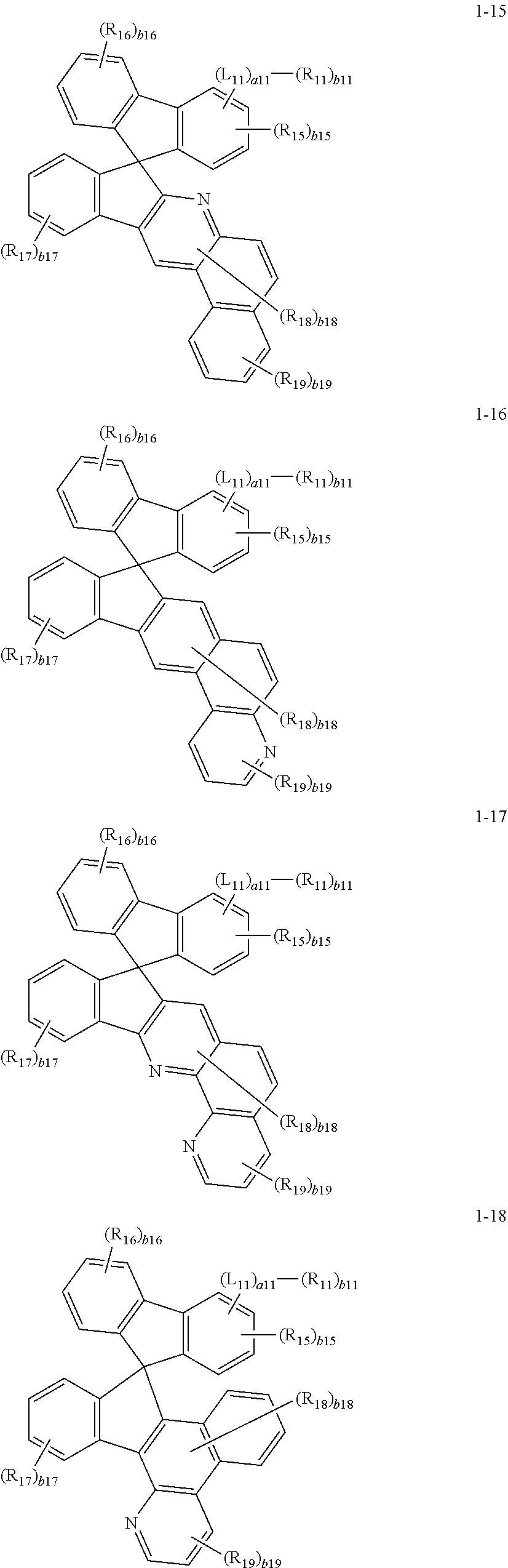
- the first material may be represented by one of the following Formulae 1-11 to 1-22.
- L 11 , a11, R 11 , R 15 to R 18 , b11 and b15 to b18 may be the same as defined above with respect to Formula 1;
- R 19 may be the same as defined in connection with R 15 in Formula 1;
- b19 may be the same as defined in connection with b15 in Formula 1.
- the first material may be represented by one of the following Formulae 1-31 to 1-42.
- L 11 , a 11 , R 11 , and b11 may be the same as defined above with respect to Formula 1.
- the first material may be one of the following Compounds 1 to 12.
- the second material (e.g., represented by Formula 2) may be represented by the following Formula 2-1.
- L 21 , a21, R 21 , R 24 to R 26 , b21 and b24 to b26 may be the same as defined above with respect to Formula 2.
- the second material may be represented by one of the following Formulae 2-11 and 2-12.
- L 21 , a21, R 21 , R 24 to R 26 , b21 and b24 to b26 may be the same as defined above with respect to Formula 2.
- the second material may be represented by one of the following Formulae 2-21 to 2-24.
- L 21 , a21, and R 21 may be the same as defined above with respect to Formula 2;
- R 27 may be the same as defined in connection with R 21 in Formula 2.
- the second material may be one of the following Compounds 101 to 124.
- the first material may have a high charge transporting property and an appropriate triplet energy level.
- an organic light-emitting device including the first material may have a high carrier density and a large amount of excitons in an emission layer.
- the first material may include an electrochemically stable core, and thus lifespan of the organic light-emitting device including the first material may increase.
- the first material may be electrochemically more stable than a compound having an indenocarbazole moiety as a core.
- the second material may have a wide energy gap and a low charge mobility.
- the second material may help control a charge transporting property of the first material.
- An organic light-emitting device including the first material and the second material may have good charge and hole balance in an emission layer, and excitons may be evenly distributed throughout the whole emission layer. Therefore, the organic light-emitting device including the first material and the second material may have improved efficiency and lifespan characteristics.
- a weight ratio of the first material to the second material may be about 1:9 to about 9:1.
- a weight ratio of the first material to the second material may be about 2:8 to about 8:2.
- a weight ratio of the first material to the second material may be about 3:7 to about 7:3.
- a weight ratio of the first material to the second material may be about 5:5.
- the first material and the second material may be both included in the emission layer in the organic layer 150 .
- all of the first material and the second material may be a host.
- the hole transport region may be disposed between the first electrode 110 and the emission layer.
- the hole transport region may include at least one of a hole injection layer (HIL), a hole transport layer (HTL), a buffer layer, and an electron blocking layer (EBL).
- HIL hole injection layer
- HTL hole transport layer
- EBL electron blocking layer
- EIL electron injection layer
- the hole transport region may have a single-layered structure formed of a single material, a single-layered structure formed of a plurality of different materials, or a multi-layered structure having a plurality of layers formed of a plurality of different materials.
- the hole transport region may have a single-layered structure formed of a plurality of different materials, or a structure of hole injection layer/hole transport layer, a structure of hole injection layer/hole transport layer/buffer layer, a structure of hole injection layer/buffer layer, a structure of hole transport layer/buffer layer, a structure of hole injection layer/hole transport layer/electron blocking layer, or a structure of hole transport layer/electron blocking layer, wherein layers of each of the structures are sequentially stacked from the first electrode 110 in this stated order.
- the hole injection layer may be formed on the first electrode 110 by using various methods, e.g., vacuum deposition, spin coating, casting, a Langmuir-Blodgett (LB) method, ink-jet printing, laser-printing, or laser-induced thermal imaging (LITI).
- various methods e.g., vacuum deposition, spin coating, casting, a Langmuir-Blodgett (LB) method, ink-jet printing, laser-printing, or laser-induced thermal imaging (LITI).
- LB Langmuir-Blodgett
- LITI laser-induced thermal imaging
- the vacuum deposition may be performed at a deposition temperature in a range of about 100° C. to about 500° C., at a vacuum degree in a range of about 10 ⁇ 8 torr to about 10 ⁇ 3 torr, and/or at a deposition rate in a range of about 0.01 ⁇ /sec to about 100 ⁇ /sec, in consideration of a compound for forming a hole injection layer and a structure of a desired hole injection layer.
- the spin coating may be performed at a coating rate in a range of about 2,000 rpm to about 5,000 rpm and/or at a temperature in a range of about 80° C. to about 200° C., in consideration of a compound for forming a hole injection layer and a structure of a desired hole injection layer.
- the hole transport layer may be formed on the first electrode 110 or on the hole injection layer by using various methods, e.g., vacuum deposition, spin coating, casting, a LB method, ink-jet printing, laser-printing, or LITI.
- vacuum deposition spin coating
- the deposition conditions or the coating conditions may be inferred based on the deposition conditions or the coating conditions for forming the hole injection layer.
- the hole transport region may include, e.g., at least one from m-MTDATA, TDATA, 2-TNATA, NPB, ⁇ -NPB, TPD, Spiro-TPD, Spiro-NPB, a methylated NPB, TAPC, HMTPD, 4,4′,4′′-tris(N-carbazolyl)triphenylamine (TCTA), polyaniline/dodecyla benzenesulfonic acid (Pani/DBSA), poly(3,4-ethylenedioxythiophene)/poly(4-styrenesulfonate) (PEDOT/PSS), polyaniline/camphor sulfonicacid (Pani/CSA), (polyaniline)/poly(4-styrenesulfonate) (PANI/PSS), a compound represented by Formula 201, and a compound represented by Formula 202:
- L 201 to L 205 may each independently be selected from a substituted or unsubstituted C 3 -C 10 cycloalkylene, a substituted or unsubstituted heterocycloalkylene, a substituted or unsubstituted C 3 -C 10 cycloalkenylene, a substituted or unsubstituted hetetocycloalkenylene, a substituted or unsubstituted C 6 -C 60 arylene, a substituted or unsubstituted heteroarylene, a substituted or unsubstituted divalent non-aromatic condensed polycyclic group, and a substituted or unsubstituted divalent non-aromatic condensed heteropolycyclic group;
- xa1 to xa4 may each independently be selected from 0, 1, 2, and 3;
- xa5 is selected from 1, 2, 3, 4, and 5;
- R 201 to R 205 may each independently be the same as defined in connection with R 11 in the present specification.
- the compound represented by Formula 201 may be represented by Formula 201A:
- the compound represented by Formula 201 may be represented by Formula 201A-1:
- the compound represented by Formula 202 may be represented by Formula 202A:
- L 201 to L 203 , xa1 to xa3, xa5, and R 202 to R 204 may be the same as defined in the present specification, and R 211 and R 212 may be the same as defined in connection with R 203 , and R 213 to R 216 may each independently be selected from a hydrogen, a deuterium, —F, —Cl, —Br, —I, a hydroxyl group, a cyano group, a nitro group, an amino group, an amidino group, a hydrazine group, a hydrazone group, a carboxylic acid or a salt thereof, a sulfonic acid or a salt thereof, a phosphoric acid or a salt thereof, a C 1 -C 60 alkyl group, a C 2 -C 60 alkenyl group, a C 2 -C 60 alkynyl group, a C 1 -
- L 201 to L 203 may each independently be selected from:
- xa1 to xa3 may each independently be 0 or 1;
- R 202 to R 204 , R 211 , and R 212 may each independently be selected from:
- R 213 and R 214 may each independently be selected from:
- a C 1 -C 20 alkyl group and a C 1 -C 20 alkoxy group each substituted with at least one selected from a deuterium, —F, —Cl, —Br, —I, a hydroxyl group, a cyano group, a nitro group, an amino group, an amidino group, a hydrazine group, a hydrazone group, a carboxylic acid or a salt thereof, a sulfonic acid or a salt thereof, a phosphoric acid or a salt thereof, a phenyl group, a naphthyl group, a fluorenyl group, a spiro-fluorenyl group, a benzofluorenyl group, a dibenzofluorenyl group, a phenanthrenyl group, an anthracenyl group, a pyrenyl group, a chrysenyl group, a pyridinyl group
- R 215 and R 216 may each independently be selected from:
- a deuterium —F, —Cl, —Br, —I, a hydroxyl group, a cyano group, a nitro group, an amino group, an amidino group, a hydrazine group, a hydrazone group, a carboxylic acid or a salt thereof, a sulfonic acid or a salt thereof, a phosphoric acid or a salt thereof, a C 1 -C 20 alkyl group, and a C 1 -C 20 alkoxy group;
- a C 1 -C 20 alkyl group and a C 1 -C 20 alkoxy group each substituted with at least one selected from a deuterium, —F, —Cl, —Br, —I, a hydroxyl group, a cyano group, a nitro group, an amino group, an amidino group, a hydrazine group, a hydrazone group, a carboxylic acid or a salt thereof, a sulfonic acid or a salt thereof, a phosphoric acid or a salt thereof, a phenyl group, a naphthyl group, a fluorenyl group, a spiro-fluorenyl group, a benzofluorenyl group, a dibenzofluorenyl group, a phenanthrenyl group, an anthracenyl group, a pyrenyl group, a chrysenyl group, a pyridinyl group
- xa5 may be 1 or 2.
- R 213 and R 214 may be fused to each other and form a saturated or unsaturated ring.
- the compound represented by Formula 201 and the compound represented by Formula 202 may include Compounds HT1 to HT20 below:
- a thickness of the hole transport region may be in a range of about 100 ⁇ to about 10,000 ⁇ , e.g., about 100 ⁇ to about 2,000 ⁇ .
- a thickness of the hole injection layer may be in a range of about 100 ⁇ to about 10,000 ⁇ , and, e.g., about 100 ⁇ to about 1,000 ⁇
- a thickness of the hole transport layer may be in a range of about 50 ⁇ to about 2,000 ⁇ , and, e.g., about 100 ⁇ to about 1,500 ⁇ .
- thicknesses of the hole transport region, the hole injection layer, and the hole transport layer are within these ranges described above, hole transporting properties may be satisfactory without a substantial increase in a driving voltage.
- the hole transport region may further include a charge-generating material to help improve conductive properties in addition to the mentioned materials above.
- the charge-generating material may be homogeneously or non-homogeneously dispersed throughout the hole transport region.
- the charge-generating material may be, e.g., a p-dopant.
- the p-dopant may include one selected from a quinone derivative, a metal oxide, and a cyano group-containing compound, but it is not limited thereto.
- a quinone derivative such as tetracyanoquinonedimethane (TCNQ) or 2,3,5,6-tetrafluoro-tetracyano-1,4-benzoquinonedimethane (F4-TCNQ)
- a metal oxide such as a tungsten oxide or a molybdenum oxide
- Compound HT-D1 illustrated below Compound HT-D1 illustrated below.
- the hole transport region may further include at least one selected from a buffer layer and an electron blocking layer, in addition to the hole injection layer and the hole transport layer.
- the buffer layer may compensate an optical resonance distance according to a wavelength of light emitted from the emission layer, and light-emission efficiency of an organic light-emitting device thus prepared may be improved.
- a material included in the buffer layer may be the same with a material that may be included in the hole transport region.
- the electron blocking layer prevents injection of electrons from the electron transport region.
- An emission layer may be formed on the first electrode 110 or the hole transport region by using various methods, e.g., vacuum deposition, spin coating, casting, a LB method, ink-jet printing, laser-printing, or laser-induced thermal imaging.
- deposition and coating conditions for the emission layer may be determined by referring to the deposition and coating conditions for the hole injection layer.
- the emission layer may include a host and a dopant.
- the host may include the first material and the second material.
- the dopant may be included in an amount of, e.g., about 0.01 part to about 15 parts by weight, based on 100 parts by weight of the host.
- a thickness of the emission layer may be about 100 ⁇ to about 1,000 ⁇ , e.g., about 200 ⁇ to about 600 ⁇ . When a thickness of the emission layer is within this range, light-emission characteristics of the emission layer may be excellent without a substantial increase in a driving voltage.
- the dopant may include, e.g., a phosphorescent dopant.
- the phosphorescent dopant may include, e.g., an organometallic compound including one of iridium (Ir), platinum (Pt), osmium (Os), titanium (Ti), zirconium (Zr), hafnium (Hf), europium (Eu), terbium (Tb), thulium (Tm), rhodium (Rh), and copper (Cu).
- an organometallic compound including one of iridium (Ir), platinum (Pt), osmium (Os), titanium (Ti), zirconium (Zr), hafnium (Hf), europium (Eu), terbium (Tb), thulium (Tm), rhodium (Rh), and copper (Cu).
- the phosphorescent dopant may include an organometallic compound represented by the following Formula 401.
- M may be selected from, e.g., iridium (Ir), platinum (Pt), osmium (Os), titanium (Ti), zirconium (Zr), hafnium (Hf), europium (Eu), terbium (Tb), thulium (Tm), rhodium (Rh), and copper (Cu);
- X 401 to X 404 may each independently be, e.g., nitrogen or carbon;
- rings A 401 and A 402 may each independently be selected from or include, e.g., a substituted or unsubstituted benzene, a substituted or unsubstituted naphthalene, a substituted or unsubstituted fluorene, a substituted or unsubstituted spiro-fluorene, a substituted or unsubstituted indene, a substituted or unsubstituted pyrrole, a substituted or unsubstituted thiophene, a substituted or unsubstituted furan, a substituted or unsubstituted imidazole, a substituted or unsubstituted pyrazole, a substituted or unsubstituted thiazole, a substituted or unsubstituted isothiazole, a substituted or unsubstituted oxazole, a substituted or unsubstituted isoxazole
- a deuterium —F, —Cl, —Br, —I, a hydroxyl group, a cyano group, a nitro group, an amino group, an amidino group, a hydrazine group, a hydrazone group, a carboxylic acid or a salt thereof, a sulfonic acid or a salt thereof, a phosphoric acid or a salt thereof, a C 1 -C 60 alkyl group, a C 2 -C 60 alkenyl group, a C 2 -C 60 alkynyl group, and a C 1 -C 60 alkoxy group;
- a C 1 -C 60 alkyl group, a C 2 -C 60 alkenyl group, a C 2 -C 60 alkynyl group, and a C 1 -C 60 alkoxy group each substituted with at least one selected from a deuterium, —F, —Cl, —Br, —I, a hydroxyl group, a cyano group, a nitro group, an amino group, an amidino group, a hydrazine group, a hydrazone group, a carboxylic acid or a salt thereof, a sulfonic acid or a salt thereof, a phosphoric acid or a salt thereof, a C 3 -C 10 cycloalkyl group, a C 1 -C 10 heterocycloalkyl group, a C 3 -C 10 cycloalkenyl group, a C 1 -C 10 heterocycloalkenyl group, a C 6 -C 60 aryl group, a
- L 401 may be, e.g., an organic ligand
- xc1 may be, e.g., 1, 2, or 3;
- xc2 may be, e.g., 0, 1, 2, or 3.
- L 401 may be, e.g., a monovalent, divalent, or trivalent organic ligand.
- L 401 may be selected from, e.g., a halogen ligand (for example, Cl or F), a diketone ligand (for example, acetylacetonate, 1,3-diphenyl-1,3-propandionate, 2,2,6,6-tetramethyl-3,5-heptanedionate, or hexafluoroacetonate), a carboxylic acid ligand (for example, picolinate, dimethyl-3-pyrazolecarboxylate, or benzoate), a carbon monoxide ligand, an isonitrile ligand, a cyano ligand, and a phosphorus ligand (for example, phosphine or phosphite).
- a halogen ligand for example, Cl or F
- a diketone ligand for example, acety
- a 401 and A 402 may be respectively and directly linked to A 401 and A 402 of a different neighboring ligand or may link to A 401 and A 402 of a different neighboring ligand via a linking group (e.g. a C 1 -C 5 alkylene group, —N(R′)— (where, R′ is a C 1 -C 10 alkyl group or a C 6 -C 20 aryl group), or —C( ⁇ O)—) therebetween.
- a linking group e.g. a C 1 -C 5 alkylene group, —N(R′)— (where, R′ is a C 1 -C 10 alkyl group or a C 6 -C 20 aryl group), or —C( ⁇ O)—
- the phosphorescent dopant may include at least one of Compounds PD1 to PD74.
- the phosphorescent dopant may include PtOEP.
- the emission layer may be patterned into a red emission layer, a green emission layer, or a blue emission layer.
- the emission layer may have a stacked structure of a red emission layer, a green emission layer, and/or a blue emission layer, and thus white light may be emitted from the emission layer.
- the electron transport region may be disposed on the emission layer.
- the electron transport region may include at least one of a hole blocking layer, an electron transport layer (ETL), and an electron injection layer.
- a hole blocking layer may include at least one of a hole blocking layer, an electron transport layer (ETL), and an electron injection layer.
- ETL electron transport layer
- the electron transport region may have a structure of electron transport layer/electron injection layer or a structure of hole blocking layer/electron transport layer/electron injection layer, wherein layers of each structure are sequentially stacked on from the emission layer in the stated order.
- the electron transport region may include a hole blocking layer.
- the hole blocking layer may be included to help prevent diffusion of triplet exitons or holes to an electron transport layer when a phosphorescent dopant is included in the emission layer.
- the hole blocking layer may be formed on the emission layer by using various methods, e.g., vacuum deposition, spin coating, casting, a Langmuir-Blodgett (LB) method, ink-jet printing, laser-printing, or laser-induced thermal imaging (LITI).
- vacuum deposition spin coating
- LB Langmuir-Blodgett
- LITI laser-induced thermal imaging
- the deposition conditions or the coating conditions may be inferred based on the deposition conditions or the coating conditions for forming the hole injection layer.
- the hole blocking layer may include at least one selected from BCP and Bphen.
- a thickness of the hole blocking layer may be in a range of about 20 ⁇ to about 1,000 ⁇ , e.g., about 30 ⁇ to about 300 ⁇ . When the thickness of the hole blocking layer is within this range, hole blocking characteristics of the hole blocking layer may be excellent without a substantial increase in driving voltage.
- the electron transport region may include an electron transport layer.
- the electron transport layer may be formed on the emission layer by using various methods, e.g., vacuum deposition, spin coating, casting, a LB method, ink-jet printing, laser-printing, or laser-induced thermal imaging.
- vacuum deposition and coating conditions for the electron transport layer may be determined by referring to the vacuum deposition and coating conditions for the hole injection layer.
- the electron transport layer may include at least one selected from BCP and BPhen above and Alq 3 , Balq, TAZ, and NTAZ below.
- the electron transport layer may include a compound represented by Formula 601.
- a 601 may be selected from:
- L 601 may be the same as defined in connection with L 201 ;
- E 601 may be selected from:
- xe1 may be selected from 0, 1, 2, and 3;
- xe2 may be selected from 1, 2, 3, and 4.
- the electron transport layer may include a compound represented by Formula 602.
- X 611 may be N or C-(L 611 ) xe611 -R 611
- X 612 may be N or C-(L 612 ) xe612 -R 612
- X 613 may be N or C-(L 613 ) xe613 -R 613
- at least one of X 611 to X 613 may be N;
- each of L 611 to L 616 may be the same as defined in connection with L 201 ;
- R 611 to R 616 may each independently be selected from:
- xe611 to xe616 may each independently be selected from 0, 1, 2, and 3.
- a compound represented by Formula 601 and a compound represented by Formula 602 may include at least one of the following Compounds ET1 to ET15.
- a thickness of the electron transport layer may be in a range of about 100 ⁇ to about 1,000 ⁇ , e.g., about 150 ⁇ to about 500 ⁇ . When the thickness of the electron transport layer is within this range, hole transporting characteristics of the electron transport layer may be excellent without a substantial increase in driving voltage.
- the electron transport layer may further include a metal-containing material, in addition to the materials described above.
- the metal-containing material may include a Li complex.
- the Li complex may include, e.g., Compound ET-D1 (lithium quinolate, LiQ) or ET-D2.
- the electron transport region may include an electron injection layer that facilitates electron injection from the second electrode 190 .
- the electron injection layer may be formed on the electron transport layer by using various methods, e.g., vacuum deposition, spin coating, casting, a LB method, ink-jet printing, laser-printing, or LITI.
- vacuum deposition and coating conditions for the electron injection layer may be determined by referring to the vacuum deposition and coating conditions for the hole injection layer.
- the electron injection layer may include at least one selected from LiF, NaCl, CsF, Li 2 O, BaO, and LiQ.
- a thickness of the electron injection layer may be in a range of about 1 ⁇ to about 100 ⁇ , e.g., about 3 ⁇ to about 90 ⁇ . When the thickness of the electron injection layer is within this range, electron injecting characteristics of the electron injection layer may be excellent without a substantial increase in a driving voltage.
- the second electrode 190 may be disposed on the electron transport region.
- the second electrode 190 may be a cathode that is an electron injection electrode, and, in this regard, a material for forming the second electrode 190 may be a material having a low work function, and such a material may be metal, alloy, an electrically conductive compound, or a mixture thereof.
- Examples of the material for the second electrode 190 may include lithium (Li), magnesium (Mg), aluminum (Al), aluminum-lithium (Al—Li), calcium (Ca), magnesium-indium (Mg—In), or magnesium-silver (Mg—Ag).
- the material for forming the second electrode 190 may be ITO or IZO.
- the second electrode 190 may be a reflective electrode, a semi-transmissive electrode, or a transmissive electrode.
- the organic light-emitting device 10 may be included in a flat display device including a thin film transistor.
- the thin film transistor may include a gate electrode, source and drain electrodes, a gate insulating layer, and an active layer, and one of the source and drain electrodes may be electrically connected with the first electrode 110 of the organic light-emitting device 10 .
- the active layer may include crystalline silicon, amorphous silicon, an organic semiconductor, or an oxide semiconductor, but it is not limited thereto.
- a C 1 -C 60 alkyl group used herein refers to a linear or branched aliphatic monovalent hydrocarbon group having 1 to 60 carbon atoms, and examples of the C 1 -C 60 alkyl group may include a methyl group, an ethyl group, a propyl group, an isobutyl group, a sec-butyl group, a tert-butyl group, a pentyl group, an iso-amyl group, and a hexyl group.
- a C 1 -C 60 alkylene group used herein refers to a divalent group having the same structure with the C 1 -C 60 alkyl group.
- a C 1 -C 60 alkoxy group used herein refers to a monovalent group represented by —OA 101 (where, A 101 is the C 1 -C 60 alkyl group), and examples of the C 1 -C 60 alkoxy group may include a methoxy group, an ethoxy group, and an isopropyloxy group.
- a C 2 -C 60 alkenyl group used herein refers to a hydrocarbon group including at least one carbon double bond in the middle or at a terminal of the C 2 -C 60 alkyl group, and examples of the C 2 -C 60 alkenyl group may include an ethenyl group, a prophenyl group, and a butenyl group.
- a C 2 -C 60 alkenylene group used herein refers to a divalent group having the same structure with the C 2 -C 60 alkenyl group.
- a C 2 -C 60 alkynyl group used herein refers to a hydrocarbon group including at least one carbon triple bond in the middle or at a terminal of the C 2 -C 60 alkyl group, and examples of the C 2 -C 60 alkynyl group may include an ethynyl group and a propynyl group.
- a C 2 -C 60 alkynylene group used herein refers to a divalent group having the same structure with the C 2 -C 60 alkynyl group.
- a C 3 -C 10 cycloalkyl group used herein refers to a monovalent monocyclic saturated hydrocarbon group including 3 to 10 carbon atoms, and examples of the C 3 -C 10 cycloalkyl group may include a cyclopropyl group, a cyclobutyl group, a cyclopentyl group, a cyclohexyl group, and a cycloheptyl group.
- a C 3 -C 10 cycloalkylene group used herein refers to a divalent group having the same structure with the C 3 -C 10 cycloalkyl group.
- a C 1 -C 10 heterocycloalkyl group used herein refers to a monovalent monocyclic group including at least one hetero atom selected from N, O, P, and S as a ring-forming atom and 1 to 10 carbon atoms, and examples of the C 1 -C 10 heterocycloalkyl group may include a tetrahydrofuranyl group and a tetrahydrothiophenyl group.
- a C 1 -C 10 heterocycloalkylene group used herein refers to a divalent group having the same structure with the C 1 -C 10 heterocycloalkyl group.
- a C 3 -C 10 cycloalkenyl group used herein refers to a monovalent monocyclic group including 3 to 10 carbon atoms and at least one double bond in the ring of the C 3 -C 10 cycloalkenyl group, and does not have aromacity.
- Examples of the C 3 -C 10 cycloalkenyl group may include a cyclopentenyl group, a cyclohexenyl group, and a cycloheptenyl group.
- a C 3 -C 10 cycloalkenylene group used herein refers to a divalent group having the same structure with the C 3 -C 10 cycloalkenyl group.
- a C 1 -C 10 heterocycloalkenyl group used herein refers to a monovalent monocyclic group including at least one hetero atom selected from N, O, P, and S as a ring-forming atom, 1 to 10 carbon atoms, and at least one double bond in its ring.
- Examples of the C 1 -C 10 heterocycloalkenyl group may include a 2,3-hydrofuranyl group and a 2,3-hydrothiophenyl group.
- a C 1 -C 10 heterocycloalkenylene group used herein refers to a divalent group having the same structure with the C 1 -C 10 heterocycloalkenyl group.
- a C 6 -C 60 aryl group used herein refers to a monovalent group including a carbocyclic aromatic system having 6 to 60 carbon atoms
- a C 6 -C 60 arylene group used herein refers to a divalent group including a carbocyclic aromatic system having 6 to 60 carbon atoms.
- Examples of the C 6 -C 60 aryl group may include a phenyl group, a naphthyl group, an anthracenyl group, a phenanthrenyl group, a pyrenyl group, and a chrysenyl group.
- the C 6 -C 60 aryl group and the C 6 -C 60 arylene group each include two or more rings, the rings may be fused to each other.
- a C 1 -C 60 heteroaryl group used herein refers to a monovalent group having a carbocyclic aromatic system including at least one hetero atom selected from N, O, P, and S as a ring-forming atom and 1 to 6 carbon atoms.
- a C 2 -C 60 heteroarylene group used herein refers to a divalent group having a carbocyclic aromatic system including at least one hetero atom selected from N, O, P, and S as a ring-forming atom and 1 to 60 carbon atoms.
- Examples of the C 1 -C 60 heteroaryl group may include a pyridinyl group, a pyrimidinyl group, a pyrazinyl group, a pyridazinyl group, a triazinyl group, a quinolinyl group, and an isoquinolinyl group.
- the C 1 -C 60 heteroaryl group and the C 1 -C 60 heteroarylene group each include two or more rings, the rings may be fused to each other.
- a C 6 -C 60 aryloxy group used herein denotes —OA 102 (where, A 102 is the C 6 -C 60 aryl group), and a C 6 -C 60 arylthio group used herein denotes —SA 103 (where, A 103 is the C 6 -C 60 aryl group).
- a monovalent non-aromatic condensed polycyclic group used herein refers to a monovalent group (for example, having 8 to 60 carbon atoms) that has two or more rings condensed to each other, only carbon atoms as a ring forming atom, and non-aromacity in the entire molecular structure.
- Examples of the monovalent non-aromatic condensed polycyclic group may include a fluorenyl group.
- a divalent non-aromatic condensed polycyclic group used herein refers to a divalent group having the same structure with the monovalent non-aromatic condensed polycyclic group.
- a monovalent non-aromatic condensed heteropolycyclic group used herein refers to a monovalent group (for example, having 1 to 60 carbon atoms) that has two or more rings condensed to each other, has a hetero atom selected from N, O, P, and S, other than carbon atoms, as a ring forming atom, and has non-aromacity in the entire molecular structure.
- Example of the monovalent non-aromatic condensed heteropolycyclic group may include a carbazolyl group.
- a divalent non-aromatic condensed heteropolycyclic group used herein refers to a divalent group having the same structure with the monovalent non-aromatic condensed heteropolycyclic group.
- a 15 ⁇ /cm 2 (500 ⁇ ) ITO glass substrate (available from Corning Co.) was cut to a size of 50 mm ⁇ 50 mm ⁇ 0.5 mm, washed with ultrasonic waves in isopropyl alcohol and pure water for 10 minutes each, and then cleaned with UV and ozone for 10 minutes. The ITO glass substrate was then mounted on a vacuum depositor.
- 2-TNATA was deposited on the ITO anode to form a hole injection layer having a thickness of 600 ⁇ , and then NPB was deposited on the hole injection layer to form a hole transport layer having a thickness of 300 ⁇ .
- Compound 1, Compound 103, and tris-(2-phenyl pyridine) iridium (III) (hereinafter, also referred to as “Ir(ppy) 3 ”) were co-deposited on the hole transport layer at a weight ratio of 20:70:10 to form an emission layer having a thickness of 400 ⁇ . Then, Alq 3 was deposited on the emission layer at a thickness of 300 ⁇ to form an electron transport layer, and Al was deposited thereon at a thickness of 1,200 ⁇ to form a cathode electrode, thereby completing manufacture of an organic light-emitting device.
- Ir(ppy) 3 tris-(2-phenyl pyridine) iridium
- Organic light-emitting devices were manufactured in the same manner as in Example 1, except that respective compounds shown in Table 1 were used at a weight ratio shown in Table 1, instead of Compound 1 and Compound 103 in the formation of the emission layer.
- T 90 Data of current densities, efficiencies, and lifespans (T 90 ) with respect to the organic light-emitting devices prepared in Examples 1 to 18 and Comparative Examples 1 to 8 were evaluated by using an IVL measuring apparatus (Photo Research PR650, Keithley 238), and the results are shown in Table 1.
- T 90 data (@3000 nit) was time consumed for an organic light-emitting device to have 90% of brightness after driving the device compared to its initial brightness (100%).
- an organic light-emitting device may have high efficiency and long lifespan characteristics.
Landscapes
- Chemical & Material Sciences (AREA)
- Engineering & Computer Science (AREA)
- Materials Engineering (AREA)
- Physics & Mathematics (AREA)
- Spectroscopy & Molecular Physics (AREA)
- Organic Chemistry (AREA)
- Optics & Photonics (AREA)
- Electroluminescent Light Sources (AREA)
Abstract
Description


in Formula 401 may be identical to or different from each other. In Formula 401, when xc1 is 2 or greater, A401 and A402 may be respectively and directly linked to A401 and A402 of a different neighboring ligand or may link to A401 and A402 of a different neighboring ligand via a linking group (e.g. a C1-C5 alkylene group, —N(R′)— (where, R′ is a C1-C10 alkyl group or a C6-C20 aryl group), or —C(═O)—) therebetween.


Ar601-[(L601)xe1-E601]xe2 <Formula 601>


| TABLE 1 | |||||||
| Weight ratio | Current | ||||||
| First | Second | (First material: second | density | Efficiency | T90 | ||
| material | material | Dopant | material: dopant) | (mA/cm2) | (cd/A) | (h) | |
| Example 1 | 1 | 103 | Ir(ppy)3 | 25:65:10 | 10 | 46.9 | 160 |
| Example 2 | 1 | 103 | Ir(ppy)3 | 15:75:10 | 10 | 42.5 | 226 |
| Example 3 | 4 | 103 | Ir(ppy)3 | 25:65:10 | 10 | 49.3 | 110 |
| Example 4 | 4 | 103 | Ir(ppy)3 | 15:75:10 | 10 | 44.9 | 130 |
| Example 5 | 11 | 103 | Ir(ppy)3 | 25:65:10 | 10 | 51.3 | 188 |
| Example 6 | 11 | 103 | Ir(ppy)3 | 15:75:10 | 10 | 44.3 | 160 |
| Example 7 | 1 | 108 | Ir(ppy)3 | 25:65:10 | 10 | 65.5 | 220 |
| Example 8 | 1 | 108 | Ir(ppy)3 | 15:75:10 | 10 | 48.8 | 290 |
| Example 9 | 4 | 108 | Ir(ppy)3 | 25:65:10 | 10 | 56.7 | 150 |
| Example 10 | 4 | 108 | Ir(ppy)3 | 15:75:10 | 10 | 51.6 | 240 |
| Example 11 | 11 | 108 | Ir(ppy)3 | 25:65:10 | 10 | 39.6 | 105 |
| Example 12 | 11 | 108 | Ir(ppy)3 | 15:75:10 | 10 | 44.8 | 100 |
| Example 13 | 1 | 120 | Ir(ppy)3 | 25:65:10 | 10 | 46.1 | 145 |
| Example 14 | 1 | 120 | Ir(ppy)3 | 15:75:10 | 10 | 44.4 | 160 |
| Example 15 | 4 | 120 | Ir(ppy)3 | 25:65:10 | 10 | 42.0 | 115 |
| Example 16 | 4 | 120 | Ir(ppy)3 | 15:75:10 | 10 | 34.4 | 140 |
| Example 17 | 11 | 120 | Ir(ppy)3 | 25:65:10 | 10 | 24.9 | 72 |
| Example 18 | 11 | 120 | Ir(ppy)3 | 15:75:10 | 10 | 28.1 | 184 |
| Comparative | 1 | — | Ir(ppy)3 | 90:0:10 | 10 | 22.3 | 21 |
| Example 1 | |||||||
| Comparative | 4 | — | Ir(ppy)3 | 90:0:10 | 10 | 37.1 | 23 |
| Example 2 | |||||||
| Comparative | 11 | Ir(ppy)3 | 90:0:10 | 10 | 26.4 | 41 | |
| Example 3 | |||||||
| Comparative | — | 103 | Ir(ppy)3 | 0:90:10 | 10 | 5.0 | 3 |
| Example 4 | |||||||
| Comparative | — | 108 | Ir(ppy)3 | 0:90:10 | 10 | 4.6 | 6 |
| Example 5 | |||||||
| Comparative | — | 120 | Ir(ppy)3 | 0:90:10 | 10 | 4.1 | 3 |
| Example 6 | |||||||
| Comparative | Compound | 107 | Ir(ppy)3 | 25:65:10 | 10 | 21.6 | 35 |
| Example 7 | A | ||||||
| Comparative | Compound | 107 | Ir(ppy)3 | 15:75:10 | 10 | 18.3. | 60 |
| Example 8 | A | ||||||
 |
|||||||
Claims (3)


Priority Applications (1)
| Application Number | Priority Date | Filing Date | Title |
|---|---|---|---|
| US16/904,155 US11217758B2 (en) | 2014-11-05 | 2020-06-17 | Organic light-emitting device |
Applications Claiming Priority (4)
| Application Number | Priority Date | Filing Date | Title |
|---|---|---|---|
| KR10-2014-0152861 | 2014-11-05 | ||
| KR1020140152861A KR102285389B1 (en) | 2014-11-05 | 2014-11-05 | Organic light-emitting device |
| US14/706,600 US10727418B2 (en) | 2014-11-05 | 2015-05-07 | Organic light-emitting device |
| US16/904,155 US11217758B2 (en) | 2014-11-05 | 2020-06-17 | Organic light-emitting device |
Related Parent Applications (1)
| Application Number | Title | Priority Date | Filing Date |
|---|---|---|---|
| US14/706,600 Continuation US10727418B2 (en) | 2014-11-05 | 2015-05-07 | Organic light-emitting device |
Publications (2)
| Publication Number | Publication Date |
|---|---|
| US20200321538A1 US20200321538A1 (en) | 2020-10-08 |
| US11217758B2 true US11217758B2 (en) | 2022-01-04 |
Family
ID=55853626
Family Applications (2)
| Application Number | Title | Priority Date | Filing Date |
|---|---|---|---|
| US14/706,600 Active 2036-10-01 US10727418B2 (en) | 2014-11-05 | 2015-05-07 | Organic light-emitting device |
| US16/904,155 Expired - Fee Related US11217758B2 (en) | 2014-11-05 | 2020-06-17 | Organic light-emitting device |
Family Applications Before (1)
| Application Number | Title | Priority Date | Filing Date |
|---|---|---|---|
| US14/706,600 Active 2036-10-01 US10727418B2 (en) | 2014-11-05 | 2015-05-07 | Organic light-emitting device |
Country Status (2)
| Country | Link |
|---|---|
| US (2) | US10727418B2 (en) |
| KR (1) | KR102285389B1 (en) |
Families Citing this family (8)
| Publication number | Priority date | Publication date | Assignee | Title |
|---|---|---|---|---|
| KR20120100709A (en) | 2010-01-15 | 2012-09-12 | 이데미쓰 고산 가부시키가이샤 | Organic electroluminescent element |
| KR102424977B1 (en) | 2015-04-14 | 2022-07-26 | 삼성디스플레이 주식회사 | Condensed-cyclic compound and organic light emitting device comprising the same |
| KR102630644B1 (en) | 2015-12-17 | 2024-01-30 | 삼성디스플레이 주식회사 | Organic light emitting device |
| KR102643638B1 (en) * | 2016-09-13 | 2024-03-06 | 삼성디스플레이 주식회사 | Condensed-cyclic compound and organic light emitting device comprising the same |
| CN106749236B (en) * | 2016-12-06 | 2019-01-29 | 中节能万润股份有限公司 | Azaspiro-type organic electroluminescent material with dibenzocycloheptene structure and application thereof |
| WO2019120263A1 (en) * | 2017-12-21 | 2019-06-27 | 广州华睿光电材料有限公司 | Organic mixture and application thereof in organic electronic devices |
| CN108530437B (en) * | 2018-04-27 | 2020-12-04 | 陕西莱特光电材料股份有限公司 | Main luminescent material and synthesis method and application thereof |
| KR20190125937A (en) * | 2018-04-30 | 2019-11-07 | 주식회사 엘지화학 | Novel compound and organic light emitting device comprising the same |
Citations (12)
| Publication number | Priority date | Publication date | Assignee | Title |
|---|---|---|---|---|
| WO2009021126A2 (en) | 2007-08-08 | 2009-02-12 | Universal Display Corporation | Benzo-fused thiophene or benzo-fused furan compounds comprising a triphenylene group |
| KR20110002156A (en) | 2009-07-01 | 2011-01-07 | 주식회사 엘지화학 | Novel compound and organic electronic device using same |
| US20110057171A1 (en) | 2006-12-28 | 2011-03-10 | Universal Display Corporation | Long lifetime Phosphorescent Organic Light Emitting Device (OLED) Structures |
| US20110254436A1 (en) | 2010-04-18 | 2011-10-20 | National Tsing Hua University | Triphenylene based aromatic compounds and oleds utilizing the same |
| KR20110130904A (en) | 2010-05-28 | 2011-12-06 | 주식회사 두산 | Bipolar triphenylene compound and organic electroluminescent device comprising same |
| US20120077987A1 (en) | 2010-09-27 | 2012-03-29 | Semiconductor Energy Laboratory Co., Ltd. | Organic compound, light-emitting element, light-emitting device, electronic device, and lighting device |
| WO2012133653A1 (en) | 2011-03-31 | 2012-10-04 | 富士フイルム株式会社 | Charge transport material, organic electroluminescent element, and illumination device, display device, or light-emitting device characterized by using said element |
| US20130112952A1 (en) | 2010-04-28 | 2013-05-09 | Nippon Steel Chemical Co., Ltd. | Depositing premixed materials |
| US20130277656A1 (en) * | 2012-04-20 | 2013-10-24 | Semiconductor Energy Laboratory Co., Ltd. | Light-Emitting Element, Light-Emitting Device, Electronic Appliance, and Lighting Device |
| KR20130122602A (en) | 2013-10-24 | 2013-11-07 | 주식회사 엘지화학 | New compounds and organic electronic device using the same |
| KR101433822B1 (en) * | 2013-06-17 | 2014-08-27 | 삼성디스플레이 주식회사 | Organic light emitting diode device |
| US20150001488A1 (en) | 2013-07-01 | 2015-01-01 | Soo-Hyun Min | Composition and organic optoelectric device and display device |
-
2014
- 2014-11-05 KR KR1020140152861A patent/KR102285389B1/en active Active
-
2015
- 2015-05-07 US US14/706,600 patent/US10727418B2/en active Active
-
2020
- 2020-06-17 US US16/904,155 patent/US11217758B2/en not_active Expired - Fee Related
Patent Citations (16)
| Publication number | Priority date | Publication date | Assignee | Title |
|---|---|---|---|---|
| US20110057171A1 (en) | 2006-12-28 | 2011-03-10 | Universal Display Corporation | Long lifetime Phosphorescent Organic Light Emitting Device (OLED) Structures |
| WO2009021126A2 (en) | 2007-08-08 | 2009-02-12 | Universal Display Corporation | Benzo-fused thiophene or benzo-fused furan compounds comprising a triphenylene group |
| US20100237334A1 (en) | 2007-08-08 | 2010-09-23 | Universal Display Corporation | Benzo-Fused Thiophene or Bezon-Fused Furan Compounds Comprising a Triphenylene Group |
| KR20110002156A (en) | 2009-07-01 | 2011-01-07 | 주식회사 엘지화학 | Novel compound and organic electronic device using same |
| US20110254436A1 (en) | 2010-04-18 | 2011-10-20 | National Tsing Hua University | Triphenylene based aromatic compounds and oleds utilizing the same |
| US20130112952A1 (en) | 2010-04-28 | 2013-05-09 | Nippon Steel Chemical Co., Ltd. | Depositing premixed materials |
| KR20130073023A (en) | 2010-04-28 | 2013-07-02 | 유니버셜 디스플레이 코포레이션 | Depositing premixed materials |
| KR20110130904A (en) | 2010-05-28 | 2011-12-06 | 주식회사 두산 | Bipolar triphenylene compound and organic electroluminescent device comprising same |
| US20120077987A1 (en) | 2010-09-27 | 2012-03-29 | Semiconductor Energy Laboratory Co., Ltd. | Organic compound, light-emitting element, light-emitting device, electronic device, and lighting device |
| WO2012133653A1 (en) | 2011-03-31 | 2012-10-04 | 富士フイルム株式会社 | Charge transport material, organic electroluminescent element, and illumination device, display device, or light-emitting device characterized by using said element |
| US20150069332A1 (en) | 2011-03-31 | 2015-03-12 | Udc Ireland Limited | Charge transport material, oganic electroluminescent element, and illumination device, display device, or light-emitting device characterized by using said element |
| US20130277656A1 (en) * | 2012-04-20 | 2013-10-24 | Semiconductor Energy Laboratory Co., Ltd. | Light-Emitting Element, Light-Emitting Device, Electronic Appliance, and Lighting Device |
| KR101433822B1 (en) * | 2013-06-17 | 2014-08-27 | 삼성디스플레이 주식회사 | Organic light emitting diode device |
| US20140367645A1 (en) * | 2013-06-17 | 2014-12-18 | Samsung Display Co., Ltd. | Organic light emitting diode device |
| US20150001488A1 (en) | 2013-07-01 | 2015-01-01 | Soo-Hyun Min | Composition and organic optoelectric device and display device |
| KR20130122602A (en) | 2013-10-24 | 2013-11-07 | 주식회사 엘지화학 | New compounds and organic electronic device using the same |
Non-Patent Citations (2)
| Title |
|---|
| KR101433822 English Machine Translation, created Dec. 11, 2020. (Year: 2020). * |
| KR20110002156 English machine translation via KIPRIS created Oct. 25, 2017 (Year: 2017). * |
Also Published As
| Publication number | Publication date |
|---|---|
| US10727418B2 (en) | 2020-07-28 |
| KR20160054115A (en) | 2016-05-16 |
| US20160126475A1 (en) | 2016-05-05 |
| KR102285389B9 (en) | 2024-01-08 |
| US20200321538A1 (en) | 2020-10-08 |
| KR102285389B1 (en) | 2021-08-04 |
Similar Documents
| Publication | Publication Date | Title |
|---|---|---|
| US9972789B2 (en) | Organic light-emitting device | |
| US11217758B2 (en) | Organic light-emitting device | |
| US12336426B2 (en) | Organic light-emitting device | |
| US10305041B2 (en) | Organic light-emitting device | |
| US9917262B2 (en) | Organic light-emitting device | |
| US10333074B2 (en) | Organic light-emitting device | |
| US20160013427A1 (en) | Organic light-emitting device | |
| US20160028014A1 (en) | Organic light-emitting device | |
| US20170125697A1 (en) | Organic light-emitting device | |
| US9666807B2 (en) | Organic light emitting device | |
| US9825107B2 (en) | Organic light-emitting device | |
| US10825993B2 (en) | Organic light-emitting device and method of manufacturing the same | |
| US9490434B2 (en) | Organic light-emitting device | |
| US11038113B2 (en) | Organic light-emitting device | |
| US10170703B2 (en) | Condensed cyclic compound and organic light-emitting device including the same | |
| US20170133599A1 (en) | Organic light-emitting device | |
| US10186666B2 (en) | Condensed-cyclic compound and organic light emitting device including the same | |
| US10361372B2 (en) | Organic light-emitting device | |
| US20170125690A1 (en) | Organic light-emitting device | |
| US10032994B2 (en) | Organic light-emitting device | |
| US20170155054A1 (en) | Organic light-emitting device | |
| US9905771B2 (en) | Organic light-emitting device | |
| US9793496B2 (en) | Condensed-cyclic compound and organic light-emitting device including the same | |
| US10230054B2 (en) | Organic light-emitting device | |
| US9793494B2 (en) | Organic light-emitting device |
Legal Events
| Date | Code | Title | Description |
|---|---|---|---|
| FEPP | Fee payment procedure |
Free format text: ENTITY STATUS SET TO UNDISCOUNTED (ORIGINAL EVENT CODE: BIG.); ENTITY STATUS OF PATENT OWNER: LARGE ENTITY |
|
| STPP | Information on status: patent application and granting procedure in general |
Free format text: NON FINAL ACTION MAILED |
|
| STPP | Information on status: patent application and granting procedure in general |
Free format text: RESPONSE TO NON-FINAL OFFICE ACTION ENTERED AND FORWARDED TO EXAMINER |
|
| STPP | Information on status: patent application and granting procedure in general |
Free format text: FINAL REJECTION MAILED |
|
| STPP | Information on status: patent application and granting procedure in general |
Free format text: RESPONSE AFTER FINAL ACTION FORWARDED TO EXAMINER |
|
| AS | Assignment |
Owner name: SAMSUNG DISPLAY CO., LTD., KOREA, REPUBLIC OF Free format text: ASSIGNMENT OF ASSIGNORS INTEREST;ASSIGNORS:LEE, JAE-YONG;CHO, HWAN-HEE;KIM, MYEONG-SUK;REEL/FRAME:057257/0903 Effective date: 20150417 |
|
| STPP | Information on status: patent application and granting procedure in general |
Free format text: NOTICE OF ALLOWANCE MAILED -- APPLICATION RECEIVED IN OFFICE OF PUBLICATIONS |
|
| STPP | Information on status: patent application and granting procedure in general |
Free format text: PUBLICATIONS -- ISSUE FEE PAYMENT VERIFIED |
|
| STCF | Information on status: patent grant |
Free format text: PATENTED CASE |
|
| FEPP | Fee payment procedure |
Free format text: MAINTENANCE FEE REMINDER MAILED (ORIGINAL EVENT CODE: REM.); ENTITY STATUS OF PATENT OWNER: LARGE ENTITY |
|
| LAPS | Lapse for failure to pay maintenance fees |
Free format text: PATENT EXPIRED FOR FAILURE TO PAY MAINTENANCE FEES (ORIGINAL EVENT CODE: EXP.); ENTITY STATUS OF PATENT OWNER: LARGE ENTITY |
|
| STCH | Information on status: patent discontinuation |
Free format text: PATENT EXPIRED DUE TO NONPAYMENT OF MAINTENANCE FEES UNDER 37 CFR 1.362 |