US11217517B2 - Semiconductor package with a trench portion - Google Patents
Semiconductor package with a trench portion Download PDFInfo
- Publication number
- US11217517B2 US11217517B2 US16/835,915 US202016835915A US11217517B2 US 11217517 B2 US11217517 B2 US 11217517B2 US 202016835915 A US202016835915 A US 202016835915A US 11217517 B2 US11217517 B2 US 11217517B2
- Authority
- US
- United States
- Prior art keywords
- pads
- disposed
- connection terminals
- connection
- semiconductor package
- Prior art date
- Legal status (The legal status is an assumption and is not a legal conclusion. Google has not performed a legal analysis and makes no representation as to the accuracy of the status listed.)
- Active
Links
Images


Classifications
-
- H—ELECTRICITY
- H01—ELECTRIC ELEMENTS
- H01L—SEMICONDUCTOR DEVICES NOT COVERED BY CLASS H10
- H01L23/00—Details of semiconductor or other solid state devices
- H01L23/48—Arrangements for conducting electric current to or from the solid state body in operation, e.g. leads, terminal arrangements ; Selection of materials therefor
- H01L23/488—Arrangements for conducting electric current to or from the solid state body in operation, e.g. leads, terminal arrangements ; Selection of materials therefor consisting of soldered or bonded constructions
- H01L23/498—Leads, i.e. metallisations or lead-frames on insulating substrates, e.g. chip carriers
- H01L23/49811—Additional leads joined to the metallisation on the insulating substrate, e.g. pins, bumps, wires, flat leads
- H01L23/49816—Spherical bumps on the substrate for external connection, e.g. ball grid arrays [BGA]
-
- H10W20/43—
-
- H—ELECTRICITY
- H01—ELECTRIC ELEMENTS
- H01L—SEMICONDUCTOR DEVICES NOT COVERED BY CLASS H10
- H01L23/00—Details of semiconductor or other solid state devices
- H01L23/28—Encapsulations, e.g. encapsulating layers, coatings, e.g. for protection
- H01L23/31—Encapsulations, e.g. encapsulating layers, coatings, e.g. for protection characterised by the arrangement or shape
- H01L23/3107—Encapsulations, e.g. encapsulating layers, coatings, e.g. for protection characterised by the arrangement or shape the device being completely enclosed
- H01L23/3121—Encapsulations, e.g. encapsulating layers, coatings, e.g. for protection characterised by the arrangement or shape the device being completely enclosed a substrate forming part of the encapsulation
-
- H—ELECTRICITY
- H01—ELECTRIC ELEMENTS
- H01L—SEMICONDUCTOR DEVICES NOT COVERED BY CLASS H10
- H01L23/00—Details of semiconductor or other solid state devices
- H01L23/48—Arrangements for conducting electric current to or from the solid state body in operation, e.g. leads, terminal arrangements ; Selection of materials therefor
- H01L23/488—Arrangements for conducting electric current to or from the solid state body in operation, e.g. leads, terminal arrangements ; Selection of materials therefor consisting of soldered or bonded constructions
- H01L23/498—Leads, i.e. metallisations or lead-frames on insulating substrates, e.g. chip carriers
- H01L23/49861—Lead-frames fixed on or encapsulated in insulating substrates
-
- H—ELECTRICITY
- H01—ELECTRIC ELEMENTS
- H01L—SEMICONDUCTOR DEVICES NOT COVERED BY CLASS H10
- H01L24/00—Arrangements for connecting or disconnecting semiconductor or solid-state bodies; Methods or apparatus related thereto
- H01L24/01—Means for bonding being attached to, or being formed on, the surface to be connected, e.g. chip-to-package, die-attach, "first-level" interconnects; Manufacturing methods related thereto
- H01L24/02—Bonding areas ; Manufacturing methods related thereto
- H01L24/04—Structure, shape, material or disposition of the bonding areas prior to the connecting process
- H01L24/05—Structure, shape, material or disposition of the bonding areas prior to the connecting process of an individual bonding area
-
- H—ELECTRICITY
- H01—ELECTRIC ELEMENTS
- H01L—SEMICONDUCTOR DEVICES NOT COVERED BY CLASS H10
- H01L24/00—Arrangements for connecting or disconnecting semiconductor or solid-state bodies; Methods or apparatus related thereto
- H01L24/01—Means for bonding being attached to, or being formed on, the surface to be connected, e.g. chip-to-package, die-attach, "first-level" interconnects; Manufacturing methods related thereto
- H01L24/10—Bump connectors ; Manufacturing methods related thereto
- H01L24/12—Structure, shape, material or disposition of the bump connectors prior to the connecting process
- H01L24/13—Structure, shape, material or disposition of the bump connectors prior to the connecting process of an individual bump connector
-
- H—ELECTRICITY
- H01—ELECTRIC ELEMENTS
- H01L—SEMICONDUCTOR DEVICES NOT COVERED BY CLASS H10
- H01L24/00—Arrangements for connecting or disconnecting semiconductor or solid-state bodies; Methods or apparatus related thereto
- H01L24/01—Means for bonding being attached to, or being formed on, the surface to be connected, e.g. chip-to-package, die-attach, "first-level" interconnects; Manufacturing methods related thereto
- H01L24/42—Wire connectors; Manufacturing methods related thereto
- H01L24/44—Structure, shape, material or disposition of the wire connectors prior to the connecting process
- H01L24/45—Structure, shape, material or disposition of the wire connectors prior to the connecting process of an individual wire connector
-
- H10W20/484—
-
- H10W70/479—
-
- H10W70/65—
-
- H10W72/072—
-
- H10W72/20—
-
- H10W72/30—
-
- H10W72/50—
-
- H10W72/90—
-
- H10W74/114—
-
- H10W74/117—
-
- H10W74/124—
-
- H10W90/00—
-
- H10W90/401—
-
- H10W90/701—
-
- H10W70/60—
-
- H10W70/652—
-
- H10W70/698—
-
- H10W72/07236—
-
- H10W72/07252—
-
- H10W72/07253—
-
- H10W72/07254—
-
- H10W72/073—
-
- H10W72/07335—
-
- H10W72/07338—
-
- H10W72/074—
-
- H10W72/227—
-
- H10W72/232—
-
- H10W72/234—
-
- H10W72/241—
-
- H10W72/244—
-
- H10W72/247—
-
- H10W72/248—
-
- H10W72/252—
-
- H10W72/29—
-
- H10W72/325—
-
- H10W72/352—
-
- H10W72/353—
-
- H10W72/354—
-
- H10W72/551—
-
- H10W72/59—
-
- H10W72/859—
-
- H10W72/877—
-
- H10W72/879—
-
- H10W72/884—
-
- H10W72/942—
-
- H10W72/944—
-
- H10W74/10—
-
- H10W90/291—
-
- H10W90/722—
-
- H10W90/724—
-
- H10W90/734—
-
- H10W90/754—
Definitions
- the present inventive concept relates to a semiconductor package.
- An aspect of the present inventive concept is to provide a semiconductor package capable of preventing shorts from occurring between external connection terminals of a semiconductor package.
- a semiconductor package may be disclosed.
- the semiconductor package may include a substrate having an upper surface on which a plurality of first pads are disposed and a lower surface on which a plurality of second pads, electrically connected to the plurality of first pads, are disposed.
- the semiconductor package may further include a semiconductor chip disposed on the upper surface of the substrate, the semiconductor chip having a first surface on which connection electrodes connected to a first set of the plurality of first pads are disposed and a second surface opposite to the first surface.
- the semiconductor package may include an interposer disposed on the second surface of the semiconductor chip, the interposer having an upper surface on which a plurality of first connection pads, connected to a second set of the plurality of first pads, and a plurality of second connection pads are disposed, the interposer having a lower surface opposite to the upper surface and facing the second surface of the semiconductor chip, and having a width greater than a width of the semiconductor chip in at least one direction.
- the semiconductor package may further include a plurality of connection terminals disposed on a set of the plurality of second connection pads of the interposer, and a molding material disposed on the upper surface of the substrate. The molding material covering at least the upper surface of the interposer, and having at least one trench portion exposing two or more adjacent connection terminals of the plurality of connection terminals.
- a semiconductor package may be disclosed.
- the semiconductor package may include a substrate having an upper surface and a lower surface, each of the upper surface and the lower surface being provided with a plurality of pads.
- the semiconductor package may further include a semiconductor chip disposed on the upper surface of the substrate that is electrically connected to the substrate and an interposer disposed on the semiconductor chip, and having an upper surface provided with a plurality of connection pads.
- the semiconductor package may further include a plurality of connection terminals disposed on at least a first set of the plurality of connection pads of the interposer, and a molding material disposed on the upper surface of the substrate. The molding material covering at least the upper surface of the interposer, and having at least one trench portion exposing the plurality of connection terminals.
- a second set of connection pads of the plurality of connection pads of the interposer, not provided with the plurality of connection terminals may be connected to the substrate.
- a semiconductor package may be disclosed.
- the semiconductor package may include a substrate having an upper surface and a lower surface, and each of the upper surface and the lower surface may be provided with a plurality of pads.
- the semiconductor package may further include a semiconductor chip disposed on the upper surface of the substrate that has an upper surface provided with a plurality of connection pads.
- the semiconductor package may further include a plurality of connection terminals disposed on the upper surface of the semiconductor chip that are connected to at least a subset of the plurality of connection pads, and a molding material having a trench portion covering at least the upper surface of the semiconductor chip and exposing at least a portion of the plurality of connection terminals.
- FIG. 1 is a side cross-sectional view illustrating a semiconductor package according to an embodiment of the present disclosure
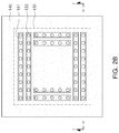
- FIGS. 2A to 2D are top plan views of the semiconductor package illustrated in FIG. 1 and illustrate a variously modified shape of a trench portion;
- FIGS. 3 to 8 are schematic side cross-sectional views illustrating a process of manufacturing the semiconductor package illustrated in FIG. 1 ;
- FIGS. 9 to 11 are side cross-sectional views illustrating a structure in which a second semiconductor package is coupled to a first semiconductor package illustrated in FIG. 1 ;
- FIGS. 12A, 12B, 13A, and 13B are cross-sectional views illustrating a state before (a) and after (b) fusion of a first upper connection terminal and a second lower connection terminal in portion “A” of FIGS. 9 and 10 to explain the effect due to a trench portion employed in an embodiment of the present disclosure;
- FIG. 14 is a graph illustrating a volume ratio in which a connection terminal could occupy in a via structure and a trench structure
- FIG. 15 is a side cross-sectional view illustrating a semiconductor package according to another embodiment of the present disclosure.
- FIG. 16 is a side cross-sectional view illustrating a state in which a semiconductor package illustrated in FIG. 15 and a second semiconductor package are coupled to each other;
- FIG. 17 is a side cross-sectional view illustrating a semiconductor package according to another embodiment of the present disclosure.
- FIG. 18 is a side cross-sectional view illustrating a state in which a semiconductor package illustrated in FIG. 17 and a second semiconductor package are coupled to each other;
- FIG. 19 is a side cross-sectional view illustrating a semiconductor package according to another embodiment of the present disclosure.
- FIG. 20 is a side cross-sectional view illustrating a state in which a semiconductor package illustrated in FIG. 19 and a second semiconductor package are coupled to each other.
- FIG. 1 is a side cross-sectional view illustrating a semiconductor package 100 A according to an embodiment of the present disclosure
- FIGS. 2A to 2D are top plan views of a semiconductor package, in which various shapes of a trench portion are illustrated.
- FIG. 1 is a cross-sectional view of the semiconductor package of FIGS. 2A to 2D , taken along line I-I′.
- a semiconductor package 100 A includes a substrate 110 , a semiconductor chip 120 , an interposer 130 , and a molding material 140 .
- lower connection terminals 150 may be further included.
- the substrate 110 may include a plurality of first pads 111 , a plurality of second pads 112 , and wirings (not shown) electrically connecting the plurality of first pads 111 to the plurality of second pads 112 .
- the substrate 110 may be a substrate for a semiconductor package such as a printed circuit board (PCB), a ceramic board, a tape wiring board, or the like.
- the substrate 110 may include a thermosetting resin such as an epoxy resin, a thermoplastic resin such as polyimide, or a photosensitive insulating layer.
- the substrate may include a material such as prepreg, an Ajinomoto build-up film (ABF), FR- 4 , Bismaleimide Triazine (BT), a Photo Imageable Dielectric (PID) resin, or the like.
- a material such as prepreg, an Ajinomoto build-up film (ABF), FR- 4 , Bismaleimide Triazine (BT), a Photo Imageable Dielectric (PID) resin, or the like.
- the plurality of first pads 111 may be disposed on an upper surface of the substrate 110 , and may be electrically and/or physically connected to the semiconductor chip 120 .
- the plurality of first pads 111 may have a horizontal width less than a horizontal width of the plurality of second pads 112 .
- the plurality of second pads 112 may be disposed on a lower surface of the substrate 110 , and may be electrically and/or physically connected to lower connection terminals 150 .
- the plurality of second pads 112 may be electrically connected to an external device such as a mainboard through the lower connection terminals 150 .
- the lower connection terminals 150 may have a flip-chip connection structure having a solder ball, a conductive bump, or a grid array such as a pin grid array, a ball grid array, or a land grid array.
- the various “pads” described herein may be connected to internal circuitry within the device to which they are connected, and may transmit signals and/or supply voltages to and/or from the device to which they are attached.
- substrate pads disposed on the package substrate may connect to rerouting and other electrical lines disposed within the package substrate, and the pads disposed on the semiconductor chips may connect to an integrated circuit on one or more of the semiconductor chips.
- the various pads described herein may generally have a planar surface at a location for connecting to a terminal for external communications outside of the device to which the pads are connected.
- the pads may be formed of a conductive material, such as metal, for example.
- the semiconductor chip 120 may have an active surface provided with connection electrodes 120 P and an inactive surface opposite to the active surface.
- the semiconductor chip 120 may be a logic chip or a memory chip.
- the semiconductor chip 120 may include a system Large scale integration (LSI), a logic circuit, a CMOS imaging sensor (CIS), a memory device such as DRAM, SRAM, flash, PRAM, ReRAM, FeRAM, MRAM, a high bandwidth memory (HBM), a Hybrid memory cubic (HMC), or the like, or a Microelectromechanical system (MEMS) device.
- LSI system Large scale integration
- CIS CMOS imaging sensor
- MRAM Microelectromechanical system
- connection members 121 may be disposed on the connection electrodes 120 P.
- the connection members 121 may include a solder ball, or a copper pillar, and the semiconductor chip 120 may be mounted on the substrate 110 in a manner of flip-chip bonding through the same.
- connection members 121 connecting the connection electrodes 120 P to at least a portion of the plurality of first pads 111 may be disposed.
- an underfill resin surrounding the connection members 121 may be formed between the active surface of the semiconductor chip 120 and the upper surface of the substrate 110 .
- the connection members 121 may be formed of conductive material, and may be, for example, conductive interconnectors (e.g., conductive wiring).
- embodiments of the present disclosure are not limited thereto, and the semiconductor chip 120 may be mounted on the substrate 110 in a manner of wire bonding in various embodiments of the present disclosure.
- the interposer 130 may include a plurality of first connection pads 131 and a plurality of second connection pads 132 and a plurality of upper connection terminals 133 (also referred to herein as a “connection terminal”), disposed on an upper surface of the interposer.
- the interposer 130 may have an upper surface and a lower surface, opposing each other.
- the interposer 130 may be a substrate including a semiconductor material or an insulating material, or a semiconductor chip.
- the interposer may include silicon, germanium, silicon-germanium, gallium-arsenic (GaAs), glass, ceramic, or the like.
- connection pads 131 and 132 are disposed on an upper surface of the interposer 130
- connection pads may be additionally disposed on a lower surface of the interposer 130
- the interposer 130 may be understood to include a wiring circuit (not shown) connecting the plurality of first and second connection pads 131 and 132 to each other.
- the interposer 130 may have a width greater than a width of the semiconductor chip 120 in at least one direction.
- the interposer 130 may have a horizontal width 130 W greater than a horizontal width 120 W of the semiconductor chip 120 .
- a space for arranging the plurality of first and second connection pads 131 and 132 may be sufficiently secured on an upper surface and/or a lower surface of the interposer 130 .
- the plurality of first connection pads 131 may be disposed close to an edge on a plane of the interposer 130 , while the plurality of second connection pads 132 may be disposed in an interior surrounded by the plurality of first connection pads 131 on a plane of the interposer 130 .
- the plurality of first connection pads 131 may be disposed on the plane of the interposer 130 and be located outside of a region overlapping the semiconductor chip in a vertical direction.
- the upper connection terminals 133 may be disposed on at least a portion (e.g., a set) of the plurality of second connection pads 132 .
- the plurality of first connection pads 131 may be connected to a portion (e.g., a set) of the plurality of first pads 111 of the substrate 110 .
- Each upper connection terminal of the upper connection terminals 133 may be, for example, a solder ball.
- the plurality of first connection pads 131 may be connected to, for example, a portion (e.g., a set) of the plurality of first pads 111 by a bonding wire WB.
- a distance d between the upper connection terminals 133 may be equal to or less than about 0.2 mm (see description of FIG. 14 ).
- the molding material 140 may cover at least the upper surface of the interposer 130 , and may have at least one trench portion 141 exposing at least two or more adjacent connection terminals 133 of the upper connection terminals 133 .
- the molding material 140 may cover an upper surface of the substrate 110 , a side surface of the semiconductor chip 120 , and an upper surface of the interposer 130 , and may fill a space between the semiconductor chip 120 and the substrate 110 .
- the molding material 140 may include an insulating material.
- an epoxy molding compound (EMC) may be used.
- the trench portion 141 may have a lower surface 141 B having a stepped portion with respect to an uppermost surface of the molding material 140 , and a wall 141 S connecting the uppermost surface of the molding material 140 to the lower surface 141 B of the trench portion 141 .
- the trench portion 141 may be formed using a laser drill, or the like.
- the lower surface 141 B of the trench portion 141 may be located at a first level that is higher in elevation than a second level of a contact interface between the upper connection terminals 133 and the plurality of second connection pads 132 .
- a portion of the molding material 140 may be in physical contact with at least a portion of a side surface of the upper connection terminals 133 .
- the lower surface 141 B of the trench portion 141 may be located at a first level exposing at least a portion of a side portion of the upper connection terminal 133 .
- the trench portion 141 may expose an upper region of the upper connection terminal 133 and at least a portion of a lower region of the upper connection terminal 133 based on a line L connecting maximum widths W 1 of the upper connection terminals 133 (see FIG. 12A ).
- an upper region of the upper connection terminals 133 and a lower region of the upper connection terminals 133 may be delineated from one another based on a horizontal line L connecting respective maximum widths W 1 of the upper connection terminals 133 .
- the wall 141 S of the trench portion 141 may be spaced apart from the adjacently disposed upper connection terminals 133 .
- the wall 141 S of the trench portion 141 may have a shape that is tapered to be closer to the adjacently disposed upper connection terminals 133 toward the lower surface 141 B of the trench portion 141 than at the uppermost surface of the molding material 140 .
- the trench portion 141 may have a plurality of bar shapes exposing the upper connection terminals 133 in a line on a plane, and the plurality of bars may be connected to each other.
- the upper connection terminals 133 may be arranged in a plurality of rows, and the at least one trench portion 141 may include a plurality of trenches arranged in each of the plurality of rows and exposing upper connection terminals that are disposed in each row.
- the upper connection terminals 133 are disposed in a form of at least one or more grids along an edge of the interposer 130 on a plane of the interposer 130
- the at least one trench portion 141 may include a plurality of trenches arranged in the form of a grid and exposing the plurality of connection terminals 133 disposed at the edge of the plane of the interposer 130 .
- FIGS. 3 to 8 are schematic side cross-sectional views illustrating a process of manufacturing a semiconductor package 100 A according to an embodiment of the present disclosure.
- a substrate 110 having an upper surface provided with a plurality of first pads 111 and a lower surface provided with a plurality of second pads 112 , electrically connected to the plurality of first pads 111 may be provided.
- the substrate 110 may further include a wiring circuit connecting the first pads 111 to the second pads 112 .
- a semiconductor chip 120 may be disposed on an upper surface of the substrate 110 .
- the connection electrodes 120 P disposed on a lower surface of the semiconductor chip 120 , may be connected to a plurality of first pads 111 on an upper surface of the substrate 110 through the connection members 121 .
- the connection members 121 may be a copper pillar, for example.
- an interposer 130 may be disposed on an upper surface of the semiconductor chip 120 .
- An upper surface of the semiconductor chip 120 and a lower surface of the interposer 130 may be bonded by an attaching member DA.
- the attaching member DA may be, for example, a non-conductive film (NCF), an anisotropic conductive film (ACF), a UV sensitive film, an instantaneous adhesive, a thermosetting adhesive, a laser curing adhesive, an ultrasonic curing adhesive, a nonconductive paste (NCP), or the like.
- a plurality of first and second connection pads 131 and 132 may be disposed on the upper surface of the interposer 130 .
- the first connection pads 131 may be disposed outside a region vertically overlapping the semiconductor chip 120 , as compared with the second connection pads 132 , on a plane of the interposer 130 , and the first connection pads 131 may be connected to the plurality of first pads 111 by a bonding wire WB.
- upper connection terminals 133 may be formed on the plurality of second connection pads 132 disposed on an inside region of the plane as compared with the first connection pads 131 .
- the upper connection terminals 133 may be a solder ball, for example.
- a molding material 140 may be formed to cover the substrate 110 , the semiconductor chip 120 , and the interposer 130 .
- the molding material 140 may be an epoxy molding compound (EMC), for example.
- EMC epoxy molding compound
- the molding material 140 may be formed to cover a plurality of upper connection terminals 133 disposed on an upper surface of the interposer 130 .
- a trench portion 141 exposing the upper connection terminals 133 may be formed in an upper portion of the molding material 140 .
- the trench portion 141 may be formed using a laser drill, or the like.
- a lower surface 141 B of the trench portion 141 may be formed to be located on a level that is higher in elevation than a level of a lower surface of the upper connection terminals 133 (when viewed in a side cross-sectional view).
- connection reliability of the upper connection terminals 133 may be improved.
- the wall 141 S of the trench portion 141 is spaced apart from the upper connection terminals 133 adjacent thereto, and may have a shape tapered to be closer to the adjacently disposed upper connection terminal 133 toward the lower surface 141 B of the trench portion 141 than at a higher portion of the molding material.
- the horizontal width of the trench portion 141 may increase from the lower most portion of the trench portion 141 to the upper most portion of the trench portion 141 .
- lower connection terminals 150 may be formed on a plurality of second pads 112 disposed on a lower surface of the substrate 110 .
- the lower connection terminals 150 may be formed using a reflow process, for example.
- FIGS. 9 to 11 are side cross-sectional views illustrating a structure in which second semiconductor packages 200 A and 200 B are coupled to the first semiconductor package 100 A illustrated in FIG. 1 .
- a second semiconductor package 200 A may include a second substrate 210 , a second semiconductor chip 220 , a second molding material 240 , and second lower connection terminals 250 .
- the second semiconductor chip 220 may be mounted on the second substrate 210 by a bonding wire 221 , for example.
- the second lower connection terminals 250 of the second semiconductor package 200 A may correspond to and may be physically/electrically connected to the first upper connection terminals 133 of the first semiconductor package 100 A.
- the first upper connection terminals 133 and the second lower connection terminals 250 may be fused to each other using a reflow process, for example.
- the second semiconductor chip 220 may be mounted on the second substrate 210 in a manner of a flip-chip.
- the second connection members 221 may be disposed between the second semiconductor chip 220 and the second substrate 210 .
- FIGS. 12A, 12B, 13A, and 13B are cross-sectional views illustrating a state before (a) and after (b) fusion of a first upper connection terminal 133 and a second lower connection terminal 250 in portion “A” of FIGS. 9 and 10 to explain the effect due to a trench portion employed in an embodiment of the present disclosure.
- a maximum width W 2 of a connection terminal C after fusion ( FIG. 12B ) of the first upper connection terminal 133 and the second lower connection terminal 250 may be further increased as compared with a maximum width W 1 of the first upper connection terminal 133 before fusion ( FIG. 12A ) of the first upper connection terminal 133 and the second lower connection terminal 250 .
- the trench portion 141 may expose an upper region of the first upper connection terminal 133 and at least a portion of a lower region of the first upper connection terminal 133 based on a line L connecting maximum widths W 1 of the first upper connection terminals 133 , from the molding material 140 . Accordingly, after fusion, an occupation space for the connection terminal C may be sufficiently secured.
- the molding material 140 may have an opening 140 H through which the first upper connection terminal 133 passes, and the maximum width HW of the opening 140 H may be less than the maximum width W 1 of the first upper connection terminal 133 .
- a maximum width W 3 of the connection terminal C after fusion may be increased rapidly.
- the first upper connection terminal 133 molten in a reflow process, is in close contact with a wall 141 ′S of a tapered via hole 141 ′ and comes up to an upper portion of the via hole 141 ′, a maximum width W 3 of the connection terminal C′ after fusion of FIG. 13B may be further increased as compared with a maximum width W 2 of the connection terminal C after fusion of FIG. 12B .
- FIG. 14 is a graph illustrating a volume ratio (a via/a trench) in which a connection terminal could occupy in a via structure and a trench structure.
- a volume of a via structure to a trench structure may be about 82%.
- a volume of a via structure to a trench structure is reduced rapidly to about 41%.
- first upper connection terminals 133 disposed adjacently, is equal to or less than about 0.2 mm, an occupation space for a connection terminal fused by applying a trench structure is secured sufficiently, so shorting between the fused connection terminals may be prevented and/or suppressed from occurring.
- FIG. 15 is a side cross-sectional view illustrating a semiconductor package 100 B according to another embodiment of the present disclosure
- FIG. 16 is a side cross-sectional view illustrating a second semiconductor package 200 A coupled to the semiconductor package 100 B illustrated in FIG. 15 .
- a semiconductor package 100 B may have a lower surface provided with connection electrodes 120 P and an upper surface provided with connection pads 122 .
- a portion of the connection pads 122 may be connected to a first pad 111 of the substrate 110 by a bonding wire WB, while a remaining portion of the connection pads 122 may be connected to upper connection terminals 123 .
- the upper connection terminals 123 may accommodate lower connection terminals of the second semiconductor package 200 A.
- FIG. 17 is a side cross-sectional view illustrating a semiconductor package 100 C according to another embodiment of the present disclosure
- FIG. 18 is a side cross-sectional view illustrating a second semiconductor package 200 A coupled to the semiconductor package 100 C illustrated in FIG. 17 .
- a semiconductor chip 120 may have an upper surface provided with connection electrodes 120 P and a lower surface opposite to the upper surface and attached to the substrate 110 .
- a portion of the connection electrodes 120 P may be connected to a first pad 111 of the substrate 110 by a bonding wire WB, while a remaining portion of the connection electrodes 120 P may be connected to upper connection terminals 123 .
- the upper connection terminals 123 may accommodate lower connection terminals of the second semiconductor package 200 A.
- FIG. 19 is a side cross-sectional view illustrating a semiconductor package 100 D according to another embodiment of the present disclosure
- FIG. 20 is a side cross-sectional view illustrating a second semiconductor package 200 A coupled to the semiconductor package 100 D illustrated in FIG. 19 .
- a semiconductor chip 120 may have a lower surface provided with connection electrodes 120 P and an upper surface provided with connection pads 122 , and may further include a through-electrode 124 connecting the connection electrodes 120 P to the connection pads 122 .
- the connection pads 122 may be connected to upper connection terminals 123 .
- the upper connection terminals 123 may accommodate lower connection terminals of the second semiconductor package 200 A, and may be electrically connected to the substrate 110 through a through-electrode 124 of the semiconductor chip 120 .
- the description of the components of the present disclosure may be referred to in the description of the same or similar components of the semiconductor package 100 A illustrated in FIG. 1 , unless specifically explained otherwise.
- a semiconductor package may be provided, capable of preventing and/or suppressing shorting between external connection terminals of a semiconductor package from occurring by introducing a trench portion securing an occupation space for the external connection terminal.
Landscapes
- Engineering & Computer Science (AREA)
- Microelectronics & Electronic Packaging (AREA)
- Power Engineering (AREA)
- Computer Hardware Design (AREA)
- Physics & Mathematics (AREA)
- Condensed Matter Physics & Semiconductors (AREA)
- General Physics & Mathematics (AREA)
- Structures Or Materials For Encapsulating Or Coating Semiconductor Devices Or Solid State Devices (AREA)
- Geometry (AREA)
Abstract
Description
Claims (18)
Applications Claiming Priority (2)
| Application Number | Priority Date | Filing Date | Title |
|---|---|---|---|
| KR10-2019-0093098 | 2019-07-31 | ||
| KR1020190093098A KR102728523B1 (en) | 2019-07-31 | 2019-07-31 | Semiconductor package |
Publications (2)
| Publication Number | Publication Date |
|---|---|
| US20210035895A1 US20210035895A1 (en) | 2021-02-04 |
| US11217517B2 true US11217517B2 (en) | 2022-01-04 |
Family
ID=74258691
Family Applications (1)
| Application Number | Title | Priority Date | Filing Date |
|---|---|---|---|
| US16/835,915 Active US11217517B2 (en) | 2019-07-31 | 2020-03-31 | Semiconductor package with a trench portion |
Country Status (3)
| Country | Link |
|---|---|
| US (1) | US11217517B2 (en) |
| KR (1) | KR102728523B1 (en) |
| CN (1) | CN112310001A (en) |
Cited By (1)
| Publication number | Priority date | Publication date | Assignee | Title |
|---|---|---|---|---|
| US20220077127A1 (en) * | 2020-09-04 | 2022-03-10 | SK Hynix Inc. | Semiconductor package including stacked semiconductor chips and method for fabricating the semiconductor package |
Families Citing this family (4)
| Publication number | Priority date | Publication date | Assignee | Title |
|---|---|---|---|---|
| JP2021177515A (en) * | 2020-05-07 | 2021-11-11 | 富士通株式会社 | Substrate unit |
| US20220399278A1 (en) * | 2021-06-11 | 2022-12-15 | Intel Corporation | Package with embedded device cavity provided by spaced interposers |
| EP4325556A4 (en) | 2022-07-08 | 2024-06-26 | Changxin Memory Technologies, Inc. | SEMICONDUCTOR PACKAGING ASSEMBLY AND PREPARATION METHOD |
| EP4325561A4 (en) | 2022-07-08 | 2024-12-11 | Changxin Memory Technologies, Inc. | SEMICONDUCTOR PACKAGING STRUCTURE AND MANUFACTURING METHODS |
Citations (15)
| Publication number | Priority date | Publication date | Assignee | Title |
|---|---|---|---|---|
| US7185426B1 (en) | 2002-05-01 | 2007-03-06 | Amkor Technology, Inc. | Method of manufacturing a semiconductor package |
| US20090127686A1 (en) | 2007-11-21 | 2009-05-21 | Advanced Chip Engineering Technology Inc. | Stacking die package structure for semiconductor devices and method of the same |
| US7749808B2 (en) | 2005-09-01 | 2010-07-06 | Micron Technology, Inc. | Stacked microelectronic devices and methods for manufacturing microelectronic devices |
| US7750455B2 (en) * | 2008-08-08 | 2010-07-06 | Stats Chippac Ltd. | Triple tier package on package system |
| US8034660B2 (en) | 2009-07-24 | 2011-10-11 | Texas Instruments Incorporated | PoP precursor with interposer for top package bond pad pitch compensation |
| US8050047B2 (en) | 2007-07-12 | 2011-11-01 | Stats Chippac Ltd. | Integrated circuit package system with flexible substrate and recessed package |
| US8884419B1 (en) | 2009-05-06 | 2014-11-11 | Marvell International Ltd. | Integrated circuit packaging configurations |
| US9070627B2 (en) | 2013-09-11 | 2015-06-30 | Broadcom Corporation | Interposer package-on-package structure |
| US9337135B2 (en) | 2014-10-08 | 2016-05-10 | Taiwan Semiconductor Manufacturing Company, Ltd. | Pop joint through interposer |
| US20170117261A1 (en) | 2014-08-22 | 2017-04-27 | Taiwan Semiconductor Manufacturing Company, Ltd. | Semiconductor packages and methods of forming the same |
| US9842798B2 (en) | 2012-03-23 | 2017-12-12 | STATS ChipPAC Pte. Ltd. | Semiconductor device and method of forming a PoP device with embedded vertical interconnect units |
| US20180053753A1 (en) | 2016-08-16 | 2018-02-22 | Freescale Semiconductor, Inc. | Stackable molded packages and methods of manufacture thereof |
| US10049964B2 (en) | 2012-03-23 | 2018-08-14 | STATS ChipPAC Pte. Ltd. | Semiconductor device and method of forming a fan-out PoP device with PWB vertical interconnect units |
| US10083903B1 (en) | 2011-06-16 | 2018-09-25 | STATS ChipPAC Pte. Ltd. | Integrated circuit packaging system with molded laser via interposer and method of manufacture thereof |
| US20200328187A1 (en) * | 2019-04-15 | 2020-10-15 | Samsung Electronics Co., Ltd. | Semiconductor package |
Family Cites Families (4)
| Publication number | Priority date | Publication date | Assignee | Title |
|---|---|---|---|---|
| JPH09260540A (en) * | 1996-03-27 | 1997-10-03 | Toshiba Corp | Method of manufacturing package base for semiconductor |
| US8492263B2 (en) * | 2007-11-16 | 2013-07-23 | Taiwan Semiconductor Manufacturing Company, Ltd. | Protected solder ball joints in wafer level chip-scale packaging |
| KR102229202B1 (en) * | 2013-11-07 | 2021-03-17 | 삼성전자주식회사 | Semicondcutor packages having trench type opening and methods for fabricating the same |
| KR101933425B1 (en) * | 2017-11-30 | 2018-12-28 | 삼성전기 주식회사 | Semiconductor package |
-
2019
- 2019-07-31 KR KR1020190093098A patent/KR102728523B1/en active Active
-
2020
- 2020-03-31 US US16/835,915 patent/US11217517B2/en active Active
- 2020-07-06 CN CN202010641308.XA patent/CN112310001A/en active Pending
Patent Citations (15)
| Publication number | Priority date | Publication date | Assignee | Title |
|---|---|---|---|---|
| US7185426B1 (en) | 2002-05-01 | 2007-03-06 | Amkor Technology, Inc. | Method of manufacturing a semiconductor package |
| US7749808B2 (en) | 2005-09-01 | 2010-07-06 | Micron Technology, Inc. | Stacked microelectronic devices and methods for manufacturing microelectronic devices |
| US8050047B2 (en) | 2007-07-12 | 2011-11-01 | Stats Chippac Ltd. | Integrated circuit package system with flexible substrate and recessed package |
| US20090127686A1 (en) | 2007-11-21 | 2009-05-21 | Advanced Chip Engineering Technology Inc. | Stacking die package structure for semiconductor devices and method of the same |
| US7750455B2 (en) * | 2008-08-08 | 2010-07-06 | Stats Chippac Ltd. | Triple tier package on package system |
| US8884419B1 (en) | 2009-05-06 | 2014-11-11 | Marvell International Ltd. | Integrated circuit packaging configurations |
| US8034660B2 (en) | 2009-07-24 | 2011-10-11 | Texas Instruments Incorporated | PoP precursor with interposer for top package bond pad pitch compensation |
| US10083903B1 (en) | 2011-06-16 | 2018-09-25 | STATS ChipPAC Pte. Ltd. | Integrated circuit packaging system with molded laser via interposer and method of manufacture thereof |
| US9842798B2 (en) | 2012-03-23 | 2017-12-12 | STATS ChipPAC Pte. Ltd. | Semiconductor device and method of forming a PoP device with embedded vertical interconnect units |
| US10049964B2 (en) | 2012-03-23 | 2018-08-14 | STATS ChipPAC Pte. Ltd. | Semiconductor device and method of forming a fan-out PoP device with PWB vertical interconnect units |
| US9070627B2 (en) | 2013-09-11 | 2015-06-30 | Broadcom Corporation | Interposer package-on-package structure |
| US20170117261A1 (en) | 2014-08-22 | 2017-04-27 | Taiwan Semiconductor Manufacturing Company, Ltd. | Semiconductor packages and methods of forming the same |
| US9337135B2 (en) | 2014-10-08 | 2016-05-10 | Taiwan Semiconductor Manufacturing Company, Ltd. | Pop joint through interposer |
| US20180053753A1 (en) | 2016-08-16 | 2018-02-22 | Freescale Semiconductor, Inc. | Stackable molded packages and methods of manufacture thereof |
| US20200328187A1 (en) * | 2019-04-15 | 2020-10-15 | Samsung Electronics Co., Ltd. | Semiconductor package |
Cited By (2)
| Publication number | Priority date | Publication date | Assignee | Title |
|---|---|---|---|---|
| US20220077127A1 (en) * | 2020-09-04 | 2022-03-10 | SK Hynix Inc. | Semiconductor package including stacked semiconductor chips and method for fabricating the semiconductor package |
| US11569216B2 (en) * | 2020-09-04 | 2023-01-31 | SK Hynix Inc. | Semiconductor package including stacked semiconductor chips and method for fabricating the semiconductor package |
Also Published As
| Publication number | Publication date |
|---|---|
| US20210035895A1 (en) | 2021-02-04 |
| KR102728523B1 (en) | 2024-11-13 |
| KR20210016119A (en) | 2021-02-15 |
| CN112310001A (en) | 2021-02-02 |
Similar Documents
| Publication | Publication Date | Title |
|---|---|---|
| US11217517B2 (en) | Semiconductor package with a trench portion | |
| CN109585390B (en) | Semiconductor package | |
| US12205939B2 (en) | Semiconductor package | |
| TWI479630B (en) | Enhanced stacked microelectronic assembly with central contacts and its system, module and configuration | |
| JP7612974B2 (en) | Electronics | |
| US9484292B2 (en) | Semiconductor package and method of forming the same | |
| US8957518B2 (en) | Molded interposer package and method for fabricating the same | |
| KR101236798B1 (en) | wafer level stack package and method for manufacturing the same | |
| TWI698966B (en) | Electronic package and manufacturing method thereof | |
| TWI496270B (en) | Semiconductor package and its manufacturing method | |
| US12255182B2 (en) | Electronic package and manufacturing method thereof | |
| US20070190690A1 (en) | Integrated circuit package system with exposed interconnects | |
| US11961795B2 (en) | Semiconductor package and package-on-package including the same | |
| EP3547364B1 (en) | Semiconductor chip and semiconductor package including the same | |
| US20180240747A1 (en) | Packaging substrate and method of fabricating the same | |
| CN103384913A (en) | Enhanced stacked microelectronic assemblies with central contacts and improved ground or power distribution | |
| KR20110099555A (en) | Stacked Semiconductor Packages | |
| US20190355667A1 (en) | Semiconductor package | |
| US20260041013A1 (en) | Semiconductor package | |
| CN112992862A (en) | Interposer and semiconductor package having the same | |
| KR102729133B1 (en) | Semiconductor package | |
| US20140117557A1 (en) | Package substrate and method of forming the same | |
| US20240421136A1 (en) | Semiconductor package | |
| US20250183239A1 (en) | Electronic package and manufacturing method thereof | |
| US20240079336A1 (en) | Semiconductor package |
Legal Events
| Date | Code | Title | Description |
|---|---|---|---|
| FEPP | Fee payment procedure |
Free format text: ENTITY STATUS SET TO UNDISCOUNTED (ORIGINAL EVENT CODE: BIG.); ENTITY STATUS OF PATENT OWNER: LARGE ENTITY |
|
| AS | Assignment |
Owner name: SAMSUNG ELECTRONICS CO., LTD., KOREA, REPUBLIC OF Free format text: ASSIGNMENT OF ASSIGNORS INTEREST;ASSIGNORS:OH, JUHYEON;CHOI, WOOJIN;REEL/FRAME:052313/0833 Effective date: 20200107 |
|
| STPP | Information on status: patent application and granting procedure in general |
Free format text: DOCKETED NEW CASE - READY FOR EXAMINATION |
|
| STPP | Information on status: patent application and granting procedure in general |
Free format text: NON FINAL ACTION MAILED |
|
| STPP | Information on status: patent application and granting procedure in general |
Free format text: RESPONSE TO NON-FINAL OFFICE ACTION ENTERED AND FORWARDED TO EXAMINER |
|
| STPP | Information on status: patent application and granting procedure in general |
Free format text: NOTICE OF ALLOWANCE MAILED -- APPLICATION RECEIVED IN OFFICE OF PUBLICATIONS |
|
| STPP | Information on status: patent application and granting procedure in general |
Free format text: PUBLICATIONS -- ISSUE FEE PAYMENT RECEIVED |
|
| STPP | Information on status: patent application and granting procedure in general |
Free format text: PUBLICATIONS -- ISSUE FEE PAYMENT VERIFIED |
|
| STCF | Information on status: patent grant |
Free format text: PATENTED CASE |
|
| MAFP | Maintenance fee payment |
Free format text: PAYMENT OF MAINTENANCE FEE, 4TH YEAR, LARGE ENTITY (ORIGINAL EVENT CODE: M1551); ENTITY STATUS OF PATENT OWNER: LARGE ENTITY Year of fee payment: 4 |