US11217455B2 - Carbon-based dielectric materials for semiconductor structure fabrication and the resulting structures - Google Patents
Carbon-based dielectric materials for semiconductor structure fabrication and the resulting structures Download PDFInfo
- Publication number
- US11217455B2 US11217455B2 US16/954,419 US201816954419A US11217455B2 US 11217455 B2 US11217455 B2 US 11217455B2 US 201816954419 A US201816954419 A US 201816954419A US 11217455 B2 US11217455 B2 US 11217455B2
- Authority
- US
- United States
- Prior art keywords
- dielectric
- layer
- conductive
- adamantane
- lines
- Prior art date
- Legal status (The legal status is an assumption and is not a legal conclusion. Google has not performed a legal analysis and makes no representation as to the accuracy of the status listed.)
- Expired - Fee Related, expires
Links
Images


Classifications
-
- H01L21/31122—
-
- H—ELECTRICITY
- H10—SEMICONDUCTOR DEVICES; ELECTRIC SOLID-STATE DEVICES NOT OTHERWISE PROVIDED FOR
- H10P—GENERIC PROCESSES OR APPARATUS FOR THE MANUFACTURE OR TREATMENT OF DEVICES COVERED BY CLASS H10
- H10P50/00—Etching of wafers, substrates or parts of devices
- H10P50/20—Dry etching; Plasma etching; Reactive-ion etching
- H10P50/28—Dry etching; Plasma etching; Reactive-ion etching of insulating materials
- H10P50/282—Dry etching; Plasma etching; Reactive-ion etching of insulating materials of inorganic materials
- H10P50/283—Dry etching; Plasma etching; Reactive-ion etching of insulating materials of inorganic materials by chemical means
- H10P50/285—Dry etching; Plasma etching; Reactive-ion etching of insulating materials of inorganic materials by chemical means of materials not containing Si, e.g. PZT or Al2O3
-
- H—ELECTRICITY
- H10—SEMICONDUCTOR DEVICES; ELECTRIC SOLID-STATE DEVICES NOT OTHERWISE PROVIDED FOR
- H10W—GENERIC PACKAGES, INTERCONNECTIONS, CONNECTORS OR OTHER CONSTRUCTIONAL DETAILS OF DEVICES COVERED BY CLASS H10
- H10W20/00—Interconnections in chips, wafers or substrates
- H10W20/01—Manufacture or treatment
- H10W20/071—Manufacture or treatment of dielectric parts thereof
- H10W20/081—Manufacture or treatment of dielectric parts thereof by forming openings in the dielectric parts
- H10W20/084—Manufacture or treatment of dielectric parts thereof by forming openings in the dielectric parts for dual-damascene structures
- H10W20/088—Manufacture or treatment of dielectric parts thereof by forming openings in the dielectric parts for dual-damascene structures involving partial etching of via holes
-
- C—CHEMISTRY; METALLURGY
- C23—COATING METALLIC MATERIAL; COATING MATERIAL WITH METALLIC MATERIAL; CHEMICAL SURFACE TREATMENT; DIFFUSION TREATMENT OF METALLIC MATERIAL; COATING BY VACUUM EVAPORATION, BY SPUTTERING, BY ION IMPLANTATION OR BY CHEMICAL VAPOUR DEPOSITION, IN GENERAL; INHIBITING CORROSION OF METALLIC MATERIAL OR INCRUSTATION IN GENERAL
- C23C—COATING METALLIC MATERIAL; COATING MATERIAL WITH METALLIC MATERIAL; SURFACE TREATMENT OF METALLIC MATERIAL BY DIFFUSION INTO THE SURFACE, BY CHEMICAL CONVERSION OR SUBSTITUTION; COATING BY VACUUM EVAPORATION, BY SPUTTERING, BY ION IMPLANTATION OR BY CHEMICAL VAPOUR DEPOSITION, IN GENERAL
- C23C16/00—Chemical coating by decomposition of gaseous compounds, without leaving reaction products of surface material in the coating, i.e. chemical vapour deposition [CVD] processes
- C23C16/22—Chemical coating by decomposition of gaseous compounds, without leaving reaction products of surface material in the coating, i.e. chemical vapour deposition [CVD] processes characterised by the deposition of inorganic material, other than metallic material
- C23C16/26—Deposition of carbon only
-
- H01L21/0271—
-
- H01L21/0337—
-
- H01L21/823431—
-
- H01L29/41791—
-
- H01L29/66795—
-
- H01L29/785—
-
- H—ELECTRICITY
- H10—SEMICONDUCTOR DEVICES; ELECTRIC SOLID-STATE DEVICES NOT OTHERWISE PROVIDED FOR
- H10D—INORGANIC ELECTRIC SEMICONDUCTOR DEVICES
- H10D30/00—Field-effect transistors [FET]
- H10D30/01—Manufacture or treatment
- H10D30/021—Manufacture or treatment of FETs having insulated gates [IGFET]
- H10D30/024—Manufacture or treatment of FETs having insulated gates [IGFET] of fin field-effect transistors [FinFET]
-
- H—ELECTRICITY
- H10—SEMICONDUCTOR DEVICES; ELECTRIC SOLID-STATE DEVICES NOT OTHERWISE PROVIDED FOR
- H10D—INORGANIC ELECTRIC SEMICONDUCTOR DEVICES
- H10D30/00—Field-effect transistors [FET]
- H10D30/60—Insulated-gate field-effect transistors [IGFET]
- H10D30/62—Fin field-effect transistors [FinFET]
- H10D30/6219—Fin field-effect transistors [FinFET] characterised by the source or drain electrodes
-
- H—ELECTRICITY
- H10—SEMICONDUCTOR DEVICES; ELECTRIC SOLID-STATE DEVICES NOT OTHERWISE PROVIDED FOR
- H10D—INORGANIC ELECTRIC SEMICONDUCTOR DEVICES
- H10D64/00—Electrodes of devices having potential barriers
- H10D64/01—Manufacture or treatment
- H10D64/017—Manufacture or treatment using dummy gates in processes wherein at least parts of the final gates are self-aligned to the dummy gates, i.e. replacement gate processes
-
- H—ELECTRICITY
- H10—SEMICONDUCTOR DEVICES; ELECTRIC SOLID-STATE DEVICES NOT OTHERWISE PROVIDED FOR
- H10D—INORGANIC ELECTRIC SEMICONDUCTOR DEVICES
- H10D64/00—Electrodes of devices having potential barriers
- H10D64/20—Electrodes characterised by their shapes, relative sizes or dispositions
- H10D64/27—Electrodes not carrying the current to be rectified, amplified, oscillated or switched, e.g. gates
- H10D64/311—Gate electrodes for field-effect devices
- H10D64/411—Gate electrodes for field-effect devices for FETs
- H10D64/511—Gate electrodes for field-effect devices for FETs for IGFETs
- H10D64/512—Disposition of the gate electrodes, e.g. buried gates
- H10D64/513—Disposition of the gate electrodes, e.g. buried gates within recesses in the substrate, e.g. trench gates, groove gates or buried gates
-
- H—ELECTRICITY
- H10—SEMICONDUCTOR DEVICES; ELECTRIC SOLID-STATE DEVICES NOT OTHERWISE PROVIDED FOR
- H10D—INORGANIC ELECTRIC SEMICONDUCTOR DEVICES
- H10D64/00—Electrodes of devices having potential barriers
- H10D64/60—Electrodes characterised by their materials
- H10D64/66—Electrodes having a conductor capacitively coupled to a semiconductor by an insulator, e.g. MIS electrodes
- H10D64/68—Electrodes having a conductor capacitively coupled to a semiconductor by an insulator, e.g. MIS electrodes characterised by the insulator, e.g. by the gate insulator
- H10D64/681—Electrodes having a conductor capacitively coupled to a semiconductor by an insulator, e.g. MIS electrodes characterised by the insulator, e.g. by the gate insulator having a compositional variation, e.g. multilayered
- H10D64/685—Electrodes having a conductor capacitively coupled to a semiconductor by an insulator, e.g. MIS electrodes characterised by the insulator, e.g. by the gate insulator having a compositional variation, e.g. multilayered being perpendicular to the channel plane
-
- H—ELECTRICITY
- H10—SEMICONDUCTOR DEVICES; ELECTRIC SOLID-STATE DEVICES NOT OTHERWISE PROVIDED FOR
- H10D—INORGANIC ELECTRIC SEMICONDUCTOR DEVICES
- H10D84/00—Integrated devices formed in or on semiconductor substrates that comprise only semiconducting layers, e.g. on Si wafers or on GaAs-on-Si wafers
- H10D84/01—Manufacture or treatment
- H10D84/0123—Integrating together multiple components covered by H10D12/00 or H10D30/00, e.g. integrating multiple IGBTs
- H10D84/0126—Integrating together multiple components covered by H10D12/00 or H10D30/00, e.g. integrating multiple IGBTs the components including insulated gates, e.g. IGFETs
- H10D84/0158—Integrating together multiple components covered by H10D12/00 or H10D30/00, e.g. integrating multiple IGBTs the components including insulated gates, e.g. IGFETs the components including FinFETs
-
- H—ELECTRICITY
- H10—SEMICONDUCTOR DEVICES; ELECTRIC SOLID-STATE DEVICES NOT OTHERWISE PROVIDED FOR
- H10D—INORGANIC ELECTRIC SEMICONDUCTOR DEVICES
- H10D84/00—Integrated devices formed in or on semiconductor substrates that comprise only semiconducting layers, e.g. on Si wafers or on GaAs-on-Si wafers
- H10D84/01—Manufacture or treatment
- H10D84/02—Manufacture or treatment characterised by using material-based technologies
- H10D84/03—Manufacture or treatment characterised by using material-based technologies using Group IV technology, e.g. silicon technology or silicon-carbide [SiC] technology
- H10D84/038—Manufacture or treatment characterised by using material-based technologies using Group IV technology, e.g. silicon technology or silicon-carbide [SiC] technology using silicon technology, e.g. SiGe
-
- H—ELECTRICITY
- H10—SEMICONDUCTOR DEVICES; ELECTRIC SOLID-STATE DEVICES NOT OTHERWISE PROVIDED FOR
- H10P—GENERIC PROCESSES OR APPARATUS FOR THE MANUFACTURE OR TREATMENT OF DEVICES COVERED BY CLASS H10
- H10P14/00—Formation of materials, e.g. in the shape of layers or pillars
- H10P14/60—Formation of materials, e.g. in the shape of layers or pillars of insulating materials
- H10P14/69—Inorganic materials
- H10P14/6902—Inorganic materials composed of carbon, e.g. alpha-C, diamond or hydrogen doped carbon
-
- H—ELECTRICITY
- H10—SEMICONDUCTOR DEVICES; ELECTRIC SOLID-STATE DEVICES NOT OTHERWISE PROVIDED FOR
- H10P—GENERIC PROCESSES OR APPARATUS FOR THE MANUFACTURE OR TREATMENT OF DEVICES COVERED BY CLASS H10
- H10P50/00—Etching of wafers, substrates or parts of devices
- H10P50/73—Etching of wafers, substrates or parts of devices using masks for insulating materials
-
- H—ELECTRICITY
- H10—SEMICONDUCTOR DEVICES; ELECTRIC SOLID-STATE DEVICES NOT OTHERWISE PROVIDED FOR
- H10P—GENERIC PROCESSES OR APPARATUS FOR THE MANUFACTURE OR TREATMENT OF DEVICES COVERED BY CLASS H10
- H10P76/00—Manufacture or treatment of masks on semiconductor bodies, e.g. by lithography or photolithography
- H10P76/20—Manufacture or treatment of masks on semiconductor bodies, e.g. by lithography or photolithography of masks comprising organic materials
-
- H—ELECTRICITY
- H10—SEMICONDUCTOR DEVICES; ELECTRIC SOLID-STATE DEVICES NOT OTHERWISE PROVIDED FOR
- H10P—GENERIC PROCESSES OR APPARATUS FOR THE MANUFACTURE OR TREATMENT OF DEVICES COVERED BY CLASS H10
- H10P76/00—Manufacture or treatment of masks on semiconductor bodies, e.g. by lithography or photolithography
- H10P76/40—Manufacture or treatment of masks on semiconductor bodies, e.g. by lithography or photolithography of masks comprising inorganic materials
- H10P76/405—Manufacture or treatment of masks on semiconductor bodies, e.g. by lithography or photolithography of masks comprising inorganic materials characterised by their composition, e.g. multilayer masks
-
- H—ELECTRICITY
- H10—SEMICONDUCTOR DEVICES; ELECTRIC SOLID-STATE DEVICES NOT OTHERWISE PROVIDED FOR
- H10P—GENERIC PROCESSES OR APPARATUS FOR THE MANUFACTURE OR TREATMENT OF DEVICES COVERED BY CLASS H10
- H10P76/00—Manufacture or treatment of masks on semiconductor bodies, e.g. by lithography or photolithography
- H10P76/40—Manufacture or treatment of masks on semiconductor bodies, e.g. by lithography or photolithography of masks comprising inorganic materials
- H10P76/408—Manufacture or treatment of masks on semiconductor bodies, e.g. by lithography or photolithography of masks comprising inorganic materials characterised by their sizes, orientations, dispositions, behaviours or shapes
- H10P76/4085—Manufacture or treatment of masks on semiconductor bodies, e.g. by lithography or photolithography of masks comprising inorganic materials characterised by their sizes, orientations, dispositions, behaviours or shapes characterised by the processes involved to create the masks
-
- H—ELECTRICITY
- H10—SEMICONDUCTOR DEVICES; ELECTRIC SOLID-STATE DEVICES NOT OTHERWISE PROVIDED FOR
- H10W—GENERIC PACKAGES, INTERCONNECTIONS, CONNECTORS OR OTHER CONSTRUCTIONAL DETAILS OF DEVICES COVERED BY CLASS H10
- H10W20/00—Interconnections in chips, wafers or substrates
- H10W20/01—Manufacture or treatment
- H10W20/031—Manufacture or treatment of conductive parts of the interconnections
- H10W20/069—Manufacture or treatment of conductive parts of the interconnections by forming self-aligned vias or self-aligned contact plugs
- H10W20/0693—Manufacture or treatment of conductive parts of the interconnections by forming self-aligned vias or self-aligned contact plugs by forming self-aligned vias
-
- H—ELECTRICITY
- H10—SEMICONDUCTOR DEVICES; ELECTRIC SOLID-STATE DEVICES NOT OTHERWISE PROVIDED FOR
- H10W—GENERIC PACKAGES, INTERCONNECTIONS, CONNECTORS OR OTHER CONSTRUCTIONAL DETAILS OF DEVICES COVERED BY CLASS H10
- H10W20/00—Interconnections in chips, wafers or substrates
- H10W20/01—Manufacture or treatment
- H10W20/071—Manufacture or treatment of dielectric parts thereof
- H10W20/081—Manufacture or treatment of dielectric parts thereof by forming openings in the dielectric parts
- H10W20/084—Manufacture or treatment of dielectric parts thereof by forming openings in the dielectric parts for dual-damascene structures
- H10W20/085—Manufacture or treatment of dielectric parts thereof by forming openings in the dielectric parts for dual-damascene structures involving intermediate temporary filling with material
-
- H—ELECTRICITY
- H10—SEMICONDUCTOR DEVICES; ELECTRIC SOLID-STATE DEVICES NOT OTHERWISE PROVIDED FOR
- H10W—GENERIC PACKAGES, INTERCONNECTIONS, CONNECTORS OR OTHER CONSTRUCTIONAL DETAILS OF DEVICES COVERED BY CLASS H10
- H10W20/00—Interconnections in chips, wafers or substrates
- H10W20/01—Manufacture or treatment
- H10W20/071—Manufacture or treatment of dielectric parts thereof
- H10W20/081—Manufacture or treatment of dielectric parts thereof by forming openings in the dielectric parts
- H10W20/084—Manufacture or treatment of dielectric parts thereof by forming openings in the dielectric parts for dual-damascene structures
- H10W20/087—Manufacture or treatment of dielectric parts thereof by forming openings in the dielectric parts for dual-damascene structures involving multiple stacked pre-patterned masks
-
- H—ELECTRICITY
- H10—SEMICONDUCTOR DEVICES; ELECTRIC SOLID-STATE DEVICES NOT OTHERWISE PROVIDED FOR
- H10W—GENERIC PACKAGES, INTERCONNECTIONS, CONNECTORS OR OTHER CONSTRUCTIONAL DETAILS OF DEVICES COVERED BY CLASS H10
- H10W20/00—Interconnections in chips, wafers or substrates
- H10W20/01—Manufacture or treatment
- H10W20/031—Manufacture or treatment of conductive parts of the interconnections
- H10W20/056—Manufacture or treatment of conductive parts of the interconnections by filling conductive material into holes, grooves or trenches
Definitions
- Embodiments of the disclosure are in the field of semiconductor structures and processing and, in particular, carbon-based dielectric materials for semiconductor structure fabrication, and the resulting structures.
- integrated circuits commonly include electrically conductive microelectronic structures, which are known in the art as vias, to electrically connect metal lines or other interconnects above the vias to metal lines or other interconnects below the vias.
- Vias are typically formed by a lithographic process.
- a photoresist layer may be spin coated over a dielectric layer, the photoresist layer may be exposed to patterned actinic radiation through a patterned mask, and then the exposed layer may be developed in order to form an opening in the photoresist layer.
- an opening for the via may be etched in the dielectric layer by using the opening in the photoresist layer as an etch mask. This opening is referred to as a via opening.
- the via opening may be filled with one or more metals or other conductive materials to form the via.
- the overlay between the vias and the overlying interconnects, and the overlay between the vias and the underlying landing interconnects generally need to be controlled to high tolerances on the order of a quarter of the via pitch.
- the overlay tolerances tend to scale with them at an even greater rate than lithographic equipment is able to keep up.
- improvements are needed in the area of via and related interconnect manufacturing technologies.
- multi-gate transistors such as tri-gate transistors
- tri-gate or other non-planar transistors are generally fabricated on either bulk silicon substrates or silicon-on-insulator substrates.
- bulk silicon substrates are preferred due to their lower cost and compatibility with the existing high-yielding bulk silicon substrate infrastructure.
- Scaling multi-gate transistors has not been without consequence, however. As the dimensions of these fundamental building blocks of microelectronic circuitry are reduced and as the sheer number of fundamental building blocks fabricated in a given region is increased, the constraints on the semiconductor processes used to fabricate these building blocks have become overwhelming. Thus, improvements are needed in the area of non-planar transistor manufacturing technologies.
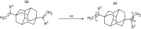
- FIG. 1 is a schematic showing an exemplary method for polymerizing disubstituted diamantane into oligomeric or polymeric (n) form, in accordance with an embodiment of the present disclosure.
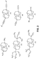
- FIG. 2 illustrates exemplary functionalized diamantanes (a)-(f) that can be polymerized (alone or with another monomer), in accordance with an embodiment of the present disclosure.
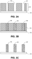
- FIGS. 3A-3C illustrate cross-sectional views representing various operations in a method of fabricating a patterned adamantane-based carbon hardmask, in accordance with an embodiment of the present disclosure.
- FIGS. 4A-4D illustrate cross-sectional views representing various operations in a method of using an adamantane-based carbon hardmask material for semiconductor structure manufacture, in accordance with an embodiment of the present disclosure.
- FIGS. 5A-5C illustrates selective etching of a gate electrode cap layer relative to a contact cap layer for self-aligned gate contact fabrication, in accordance with an embodiment of the present disclosure.
- FIGS. 6A-6H illustrate portions of integrated circuit layers representing various operations in a method of using an adamantane-based carbon hardmask material for semiconductor structure fabrication, in accordance with another embodiment of the present disclosure.
- FIG. 7A illustrates a plan view and corresponding cross-sectional view taken along the a-a′ axis of the plan view of a metallization layer, in accordance with an embodiment of the present disclosure.
- FIG. 7B illustrates a cross-sectional view of a line end or plug, in accordance with an embodiment of the present disclosure.
- FIG. 7C illustrates another cross-sectional view of a line end or plug, in accordance with an embodiment of the present disclosure.
- FIGS. 8A-8F illustrate plan views and corresponding cross-sectional views representing various operations in a plug last processing scheme, in accordance with an embodiment of the present disclosure.
- FIG. 9A illustrates a cross-sectional view of a conductive line plug having a seam therein, in accordance with an embodiment of the present disclosure.
- FIG. 9B illustrates a cross-sectional view of a stack of metallization layers including a conductive line plug at a lower metal line location, in accordance with an embodiment of the present disclosure.
- FIG. 10 illustrates a computing device in accordance with one implementation of an embodiment of the disclosure.
- FIG. 11 is an interposer implementing one or more embodiments of the disclosure.
- Embodiments described herein may be directed to front-end-of-line (FEOL) semiconductor processing and structures.
- FEOL is the first portion of integrated circuit (IC) fabrication where the individual devices (e.g., transistors, capacitors, resistors, etc.) are patterned in the semiconductor substrate or layer.
- FEOL generally covers everything up to (but not including) the deposition of metal interconnect layers. Following the last FEOL operation, the result is typically a wafer with isolated transistors (e.g., without any wires).
- Embodiments described herein may be directed to back end of line (BEOL) semiconductor processing and structures.
- BEOL is the second portion of IC fabrication where the individual devices (e.g., transistors, capacitors, resistors, etc.) are interconnected with wiring on the wafer, e.g., the metallization layer or layers.
- BEOL includes contacts, insulating layers (dielectrics), metal levels, and bonding sites for chip-to-package connections.
- contacts pads
- interconnect wires, vias and dielectric structures are formed. For modern IC processes, more than 10 metal layers may be added in the BEOL.
- Embodiments described below may be applicable to FEOL processing and structures, BEOL processing and structures, or both FEOL and BEOL processing and structures.
- an exemplary processing scheme may be illustrated using a FEOL processing scenario, such approaches may also be applicable to BEOL processing.
- an exemplary processing scheme may be illustrated using a BEOL processing scenario, such approaches may also be applicable to FEOL processing.
- One or more embodiments are directed to fabrication of a material layer, such as a hardmask layer, having properties suitable for high aspect ratio gapfill.
- the described materials may be composed of etch resistant, insulating carbon formed using oligomeric and polymeric diamondoid spin-on precursors.
- Embodiments described herein may be implemented to enable patterning techniques for fabricating semiconductor devices or structures having a pitch or 20 nanometers (20 nm) or less.
- Embodiments described herein may be implemented enable the fabrication of etch resistant fill materials.
- adamantane-based precursors multi-functional adamantanes, diamantanes, triamantanes etc.
- adamantane-based precursors are used to synthesize small oligomers and polymers.
- the resulting carbon hardmask material (referred to herein as adamantane-based carbon hardmask material) can be delivered as a material having a high percentage of sp3-hybridized carbon into features that are challenging to fill.
- FIG. 1 is a schematic showing an exemplary method for polymerizing disubstituted diamantane 100 into oligomeric or polymeric (n) form 104 , in accordance with an embodiment of the present disclosure.
- divinyl-diamantane is used as the precursor 100 .
- the process 102 for forming the oligomeric or polymeric (n) form 104 may involve use of a ruthenium (Ru) metathesis catalyst.
- the oligomeric or polymeric (n) form 104 may be suitable for delivery using, e.g., spin-coating.
- C ⁇ C bonds are included along the polymer chain or in the R1 group and provide sites for thermal, UV or other curing once the material is deposited into a selected feature.
- FIG. 2 illustrates exemplary functionalized diamantanes (a)-(f) that can be polymerized (alone or with another monomer), in accordance with an embodiment of the present disclosure.
- the oligomers or polymers resulting from treatment of the exemplary functionalized diamantanes (a)-(f), such as by process 102 may then be used as spin-coating precursors to provide high carbon content where the majority of carbon is already in a diamond-like structure.
- the molecules described herein may be used in monomeric form as volatile precursors for flowable CVD approaches for filling features.
- the monomers may be delivered to a surface where a high energy plasma or catalyst is used to initiate oligomerization at low temperature allowing newly formed molecules to flow into features prior to curing.
- FIGS. 3A-3C illustrate cross-sectional views representing various operations in a method of fabricating a patterned adamantane-based carbon hardmask, in accordance with an embodiment of the present disclosure.
- a method of fabricating a patterned adamantane-based carbon hardmask for semiconductor structure fabrication includes first forming a patterned material layer 302 above a substrate or underlying structure 300 .
- the patterned material layer 302 includes a plurality of trenches 304 formed therein.
- the patterned material layer 302 is a patterned hardmask layer.
- the patterned material layer 302 is a patterned dielectric layer.
- the trenches 304 in the patterned material layer 302 are formed using a pitch division processing and patterning scheme.
- Pitch division patterning typically refers to pitch halving, pitch quartering etc.
- Pitch division schemes may be applicable to FEOL processing, BEOL processing, or both FEOL (device) and BEOL (metallization) processing.
- optical lithography is first implemented to print unidirectional lines (e.g., either strictly unidirectional or predominantly unidirectional) in a pre-defined pitch, e.g., to form a grating structure.
- Pitch division processing is then implemented as a technique to increase line density.
- an adamantane-based carbon hardmask material 306 is formed in the trenches 304 of the patterned material layer 302 .
- the adamantane-based carbon hardmask material 306 is formed using a spin-on deposition process or a flowable chemical vapor deposition process.
- the adamantane-based carbon hardmask material 306 is formed from an adamantane monomer precursor, as described in association with FIG. 1 .
- the adamantane-based carbon hardmask material 306 is a spin-on material that has been optimized to fill high aspect ratio features.
- the adamantane-based carbon hardmask material 306 can provide for uniform fill of up to 10:1 (height to width) aspect ratio features, and even up to 20:1 or 30:1, e.g., trenches formed in a conventional hardmask layer.
- the layer 302 that now includes adamantane-based carbon hardmask material 306 therein is referred to as a two-color structure because of the dual etch properties of the film, e.g., the etch properties of the hardmask or ILD 302 and the etch properties of the adamantane-based carbon hardmask material 306 .
- the adamantane-based carbon hardmask material 306 of the two color system has a unique etch selectivity and good fill (e.g., no voids or seams).
- FIG. 3B may be used to ultimately pattern an underlying semiconductor layer.
- FIG. 3C illustrates a cross-sectional view representing an operation in a method of using an adamantane-based carbon hardmask material for semiconductor structure manufacture, in accordance with an embodiment of the present disclosure.
- the patterned material layer 302 is removed the selective to the adamantane-based carbon hardmask material 306 .
- the patterned material layer 302 is a patterned carbon-doped silicon oxide material and is removed using an etch process selective to the adamantane-based carbon hardmask material 306 .
- the pattern formed by the remaining adamantane-based carbon hardmask material 306 may then be transferred to an underlying semiconductor layer (e.g., in this case, substrate 300 is a semiconductor substrate or is a substrate having a semiconductor layer thereon). Overall, the process may effectively be viewed as a negative-tone process.
- the adamantane-based carbon hardmask material 306 is used as an etch mask for etching a semiconductor layer. In an embodiment, the adamantane-based carbon hardmask material 306 is used as an etch mask for etching a plurality of semiconductor fins in a semiconductor layer. In another embodiment, the adamantane-based carbon hardmask material 306 is used as an etch mask for etching a plurality of gate lines in a semiconductor layer. In either case, in an embodiment, the adamantane-based carbon hardmask material 306 is a sacrificial material in that it is ultimately removed, e.g., by an ash process.
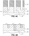
- FIGS. 4A-4D illustrate cross-sectional views representing various operations in a method of using an adamantane-based carbon hardmask material for semiconductor structure manufacture, in accordance with an embodiment of the present disclosure.
- the structure of FIG. 3B is shown having a patterned resist or hardmask layer 404 formed thereon.
- the patterned material layer 302 is a patterned hardmask layer.
- an inter-layer dielectric layer 402 is depicted above a substrate 400 , below the patterned material layer 302 having the adamantane-based carbon hardmask material 306 formed in trenches therein.
- the plurality of trenches represents all possible via locations for a metallization layer.
- an opening 406 is formed in patterned resist or hardmask layer 404 .
- a lithographic exposure is performed to form opening 406 using a relatively large exposure window.
- a trench in the center of the exposure window is selected as a via location for ultimate adamantane-based carbon hardmask material 306 clearance.
- Neighboring hardmask material portions of 302 are exposed but are not impacted by a subsequent etch process because of the dual etch selectivity of the layer 302 and the adamantane-based carbon hardmask material 306 As such, even though the neighboring regions are exposed adjacent to one or both sides of the selected trench for via formation, these regions are not impacted by a process used to remove the adamantane-based carbon hardmask material 306 from the selected via location or locations.
- the exposed one of the adamantane-based carbon hardmask material 306 regions is removed.
- the removal represents removal of the adamantane-based carbon hardmask material 306 from fewer than all of the plurality of trenches to define selected via locations for the metallization layer.
- the patterned hardmask layer 302 and remaining portions of the adamantane-based carbon hardmask material 306 are used as a mask to form one or more via trenches 408 in the ILD layer 402 to form once-patterned ILD layer 402 ′.
- the trench 408 represents an eventual interconnect line location having an associated underlying via. Accordingly, the etch process used to form trench 408 is, in one embodiment, a via selection process based on selection and removal of an adamantane-based carbon hardmask material 306 .
- the remaining portions of the adamantane-based carbon hardmask material 306 are removed.
- the patterned hardmask layer 302 is then used as a mask to form line trenches 410 in the ILD layer 402 ′ and to extend the one or more via trenches 408 to form corresponding one or more extended via trenches 408 ′ in a twice-patterned ILD layer 402 ′′.
- a dry etch process is used to pattern twice-patterned dielectric layer 402 ′′.
- the patterned hardmask layer 302 is removed.
- the one or more extended via trenches 408 ′ and the line trenches 410 are then filled with a conductive material to form a plurality of metal lines 4312 and one or more underlying conductive vias 414 .
- the plurality of metal lines 412 and one or more underlying conductive vias 414 are formed by a metal deposition and subsequent planarization process.
- FIG. 4D may subsequently be used as a foundation for forming subsequent metal line/via and ILD layers.
- the structure of FIG. 4D may represent the final metal interconnect layer in an integrated circuit.
- one or more embodiments are directed to approaches for, and structures formed from, landing a gate contact via directly on an active transistor gate. Such approaches may eliminate the need for extension of a gate line on isolation for contact purposes. Such approaches may also eliminate the need for a separate gate contact layer to conduct signals from a gate line or structure. In an embodiment, eliminating the above features is achieved by recessing contact metals in a trench contact and introducing an additional dielectric material in the process flow. The additional dielectric material is included as a trench contact dielectric cap layer with etch characteristics different from the gate dielectric material cap layer already used for trench contact alignment in a gate aligned contact process processing scheme.
- FIGS. 5A-5C illustrates selective etching of a gate electrode cap layer relative to a contact cap layer for self-aligned gate contact fabrication, in accordance with an embodiment of the present disclosure.
- a gate stack 502 is formed on or above a substrate 500 .
- First and second conductive trench contacts 514 are at first and second sides of the gate stack 502 , respectively, with an optional dielectric spacer 512 formed there between.
- a first hardmask component 510 is formed on and aligned with an uppermost surface of the gate stack 502 .
- a second hardmask component 516 is formed on and aligned with the first and second conductive trench contacts 514 .
- the first 510 and second 516 hardmask components differ in composition from one another.
- the first hardmask component 510 or the second hardmask component 516 is an adamantane-based carbon hardmask material.
- the first hardmask component 510 includes or is an adamantane-based carbon hardmask material.
- the gate stack 502 includes a high-k gate dielectric layer 504 , a workfunction gate electrode layer 506 and a conducive fill layer 508 , as is depicted.
- the first hardmask component 510 is removed from over the gate electrode 502 to form an opening 520 above gate electrode 502 . It is to be appreciated that the opening 520 may expose only a portion of the gate electrode 502 , where portions of the gate electrode 502 into and out of the page of the perspective shown remain covered by remaining unetched portions of the first hardmask component 510 . In an embodiment, the first hardmask component 510 is removed selective to the second hardmask component 516 and, if applicable, selective to the dielectric spacers 512 .
- a conductive via 522 is formed in the opening 520 in the first hardmask component and on a portion of the gate stack 502 .
- a portion of the conductive via 522 is on a portion of the second hardmask component 516 , as is depicted.
- FIGS. 6A-6H illustrate portions of integrated circuit layers representing various operations in a method of using an adamantane-based carbon hardmask material for semiconductor structure fabrication, in accordance with another embodiment of the present disclosure.
- an angled three-dimensional cross-section view is provided.
- FIG. 6A illustrates a starting point structure 600 for a subtractive via and plug process following deep metal line fabrication, in accordance with an embodiment of the present disclosure.
- structure 600 includes metal lines 602 with intervening interlayer dielectric (ILD) lines 604 .
- ILD interlayer dielectric
- the metal lines 602 are formed by patterning trenches into an ILD material (e.g., the ILD material of lines 604 ). The trenches are then filled by metal and, if needed, planarized to the top of the ILD lines 604 .
- the metal trench and fill process involves high aspect ratio features. For example, in one embodiment, the aspect ratio of metal line height to metal line width is approximately in the range of 5-10.
- FIG. 6B illustrates the structure of FIG. 6A following recessing of the metal lines, in accordance with an embodiment of the present disclosure.
- the metal lines 602 are recessed selectively to provide first level metal lines 606 .
- the recessing is performed selectively to the ILD lines 604 .
- the recessing may be performed by etching through dry etch, wet etch, or a combination thereof.
- the extent of recessing may be determined by the targeted thickness of the first level metal lines 606 for use as suitable conductive interconnect lines within a back end of line (BEOL) interconnect structure.
- BEOL back end of line
- FIG. 6C illustrates the structure of FIG. 6B following formation of an interlayer dielectric (ILD) layer, in accordance with an embodiment of the present disclosure.
- ILD interlayer dielectric
- FIG. 6D illustrates the structure of FIG. 6C following deposition and patterning of a hardmask layer, in accordance with an embodiment of the present disclosure.
- a hardmask layer 610 is formed on the ILD layer 608 .
- the hardmask layer 610 is formed with a grating pattern orthogonal to the grating pattern of the first level metal lines 606 /ILD lines 604 , as is depicted in FIG. 6D .
- the grating structure formed by the hardmask layer 610 is a tight pitch grating structure. In one such embodiment, the tight pitch is not achievable directly through conventional lithography.
- a pattern based on conventional lithography may first be formed, but the pitch may be halved by the use of spacer mask patterning. Even further, the original pitch may be quartered by a second round of spacer mask patterning. Accordingly, the grating-like pattern of the second hardmask layer 610 of FIG. 6D may have hardmask lines spaced at a constant pitch and having a constant width.
- FIG. 6E illustrates the structure of FIG. 6D following trench formation defined using the pattern of the hardmask of FIG. 6D , in accordance with an embodiment of the present disclosure.
- the exposed regions (i.e., unprotected by 610 ) of the ILD layer 608 are etched to form trenches 612 and patterned ILD layer 614 .
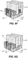
- FIG. 6F illustrates the structure of FIG. 6E following an adamantane-based carbon hardmask material formation, in accordance with an embodiment of the present disclosure.
- an adamantane-based carbon hardmask material 616 A, 616 B and 616 C is formed in possible via locations above exposed portions of the recessed metal lines 606 .
- the adamantane-based carbon hardmask material 616 A, 616 B and 616 C is formed laterally adjacent to the ILD lines 604 .
- the hardmask layer 610 may be removed from the patterned ILD layer 614 .
- FIG. 6G illustrates the structure of FIG. 6F following removal of portions of the adamantane-based carbon hardmask material to reveal selected via locations. For example, portions 616 A and 616 C of the adamantane-based carbon hardmask material are removed in select via locations. On the other hand, remaining adamantane-based carbon hardmask material 616 B is retained in locations not selected for via formation.
- the etch characteristics of the portions 616 A and 616 C of the adamantane-based carbon hardmask material enable highly selective removal of the portions 616 A and 616 C of the adamantane-based carbon hardmask material relative to the ILD lines 604 and the ILD lines 614 .
- the difference in etch characteristics between the portions 616 A and 616 C of the adamantane-based carbon hardmask material relative to the ILD lines 604 and the ILD lines 614 enables use of a wider or more relaxed lithographic process, allowing for some overlap and exposure of portions of the ILD lines 604 and/or the ILD lines 614 .
- the resulting structure includes up to three different dielectric material regions (ILD lines 604 +ILD lines 614 +remaining adamantane-based carbon hardmask material 616 B) in a single plane of the metallization structure.
- the ILD lines 604 and ILD lines 614 are composed of a same material.
- the ILD lines 604 , and the ILD lines 614 are composed of different ILD materials.
- the remaining adamantane-based carbon hardmask material 616 B is composed of an adamantane-based carbon hardmask material, examples of which are described above, and is different from the material of the ILD lines 604 and the ILD lines 614 .
- a vertical seam between the materials of ILD lines 604 and ILD lines 614 e.g., seam 697
- the remaining adamantane-based carbon hardmask material 616 B e.g., seam 698
- ILD lines 614 and the remaining adamantane-based carbon hardmask material 616 B e.g., seam 699
- FIG. 6H illustrates the structure of FIG. 6G following metal line and via formation, in accordance with an embodiment of the present disclosure.
- metal lines 622 and vias 624 are formed upon metal fill of the openings of FIG. 6G .
- the metal lines 622 are coupled to the underlying metal lines 606 by the vias 624 .
- the openings are filled in a damascene approach or a bottom-up fill approach to provide the structure shown in FIG. 6H .
- the metal (e.g., copper and associated barrier and seed layers) deposition to form metal lines and vias in the above approach may be that typically used for standard back end of line (BEOL) processing.
- BEOL back end of line
- the ILD lines 614 may be removed to provide air gaps between the resulting metal lines 624 .
- the remaining adamantane-based carbon hardmask material 616 B is retained in the final structure of FIG. 6H , as is depicted in FIG. 6H .
- the structure of FIG. 6H may subsequently be used as a foundation for forming subsequent metal line/via and ILD layers.
- the structure of FIG. 6H may represent the final metal interconnect layer in an integrated circuit.
- the above process operations may be practiced in alternative sequences, not every operation need be performed and/or additional process operations may be performed.
- the resulting structures enable fabrication of vias that are directly centered on underlying metal lines. That is, the vias may be wider than, narrower than, or the same thickness as the underlying metal lines, e.g., due to non-perfect selective etch processing. Nonetheless, in an embodiment, the centers of the vias are directly aligned (match up) with the centers of the metal lines.
- the ILD used to select which plugs and vias will likely be very different from the primary ILD and will be perfectly self-aligned in both directions.
- offset due to conventional lithography/dual damascene patterning that must otherwise be tolerated is not a factor for the resulting structures described herein.
- self-aligned fabrication by the subtractive approach may be complete at this stage.
- a next layer fabricated in a like manner likely requires initiation of the entire process once again.
- other approaches may be used at this stage to provide additional interconnect layers, such as conventional dual or single damascene approaches.
- FIG. 7A illustrates a plan view and corresponding cross-sectional view taken along the a-a′ axis of the plan view of a metallization layer, in accordance with an embodiment of the present disclosure.
- FIG. 7B illustrates a cross-sectional view of a line end or plug, in accordance with an embodiment of the present disclosure.
- FIG. 7C illustrates another cross-sectional view of a line end or plug, in accordance with an embodiment of the present disclosure.
- a metallization layer 700 includes metal lines 702 formed in a dielectric layer 704 .
- the metal lines 702 may be coupled to underlying vias 703 .
- the dielectric layer 704 may include line end or plug regions 705 .
- a line end or plug region 705 of a dielectric layer 704 may be fabricated by patterning a hardmask layer 710 on the dielectric layer 704 and then etching exposed portions of the dielectric layer 704 .
- the exposed portions of the dielectric layer 704 may be etched to a depth suitable to form a line trench 706 or further etched to a depth suitable to form a via trench 708 .
- two vias adjacent opposing sidewalls of the line end or plug 705 may be fabricated in a single large exposure 716 to ultimately form line trenches 712 and via trenches 714 .
- one or more embodiments described herein include implementation of a process flow involving construction of a line end dielectric (plug) after a trench and via patterning process.
- one or more embodiments described herein are directed to approaches for building non-conductive spaces or interruptions between metals lines (referred to as “line ends,” “plugs” or “cuts”) and, in some embodiments, associated conductive vias.
- Conductive vias by definition, are used to land on a previous layer metal pattern.
- embodiments described herein enable a more robust interconnect fabrication scheme since alignment by lithography equipment is relied on to a lesser extent. Such an interconnect fabrication scheme can be used to relax constraints on alignment/exposures, can be used to improve electrical contact (e.g., by reducing via resistance), and can be used to reduce total process operations and processing time otherwise required for patterning such features using conventional approaches.
- FIGS. 8A-8F illustrate plan views and corresponding cross-sectional views representing various operations in a plug last processing scheme, in accordance with an embodiment of the present disclosure.
- a method of fabricating an integrated circuit structure includes forming a line trench 806 in an upper portion 804 of an interlayer dielectric (ILD) material layer 802 formed above an underlying metallization layer 800 .
- a via trench 808 is formed in a lower portion 810 of the ILD material layer 802 .
- the via trench 808 exposes a metal line 812 of the underlying metallization layer 800 .
- a sacrificial material 814 is formed above the ILD material layer 802 and in the line trench 806 and the via trench 808 .
- the sacrificial material 814 may have a hardmask 815 formed thereon, as is depicted in FIG. 8B .
- the sacrificial material 814 is patterned to break a continuity of the sacrificial material 814 in the line trench 806 , e.g., to provide an opening 816 in the sacrificial material 814 .
- the opening 816 in the sacrificial material 814 is filled with a dielectric material to form a dielectric plug 818 .
- the hardmask 815 is removed to provide the dielectric plug 818 having an upper surface 820 above an upper surface 822 of the ILD material 802 , as is depicted in FIG. 8D .
- the sacrificial material 814 is removed to leave the dielectric plug 818 to remain.
- filling the opening 816 of the sacrificial material 814 with the dielectric material includes filling with an adamantane-based carbon hardmask material.
- filling the opening 814 of the sacrificial material 816 with the adamantane-based carbon hardmask material includes filling using a spin-on process or a flowable chemical vapor deposition process.
- the line trench 806 and the via trench 808 are filled with a conductive material 824 .
- the conductive material 824 is formed above and over the dielectric plug 818 and the ILD layer 802 , as is depicted.
- the conductive material 824 and the dielectric plug 818 are planarized to provide a planarized dielectric plug 818 ′ breaking a continuity of the conductive material 824 in the line trench 806 .
- an integrated circuit structure 850 includes an inter-layer dielectric (ILD) layer 802 above a substrate.
- a conductive interconnect line 824 is in a trench 806 in the ILD layer 802 .
- the conductive interconnect line 824 has a first portion 824 A and a second portion 824 B, the first portion 824 A laterally adjacent to the second portion 824 B.
- a dielectric plug 818 ′ is between and laterally adjacent to the first 824 A and second 824 B portions of the conductive interconnect line 824 .
- the conductive interconnect line 824 includes a conductive barrier liner and a conductive fill material, exemplary materials for which are described above.
- the conductive fill material includes cobalt.
- the dielectric plug 818 ′ includes an adamantane-based carbon hardmask material. In an embodiment, the dielectric plug 818 ′ is in direct contact with the first 824 A and second 824 B portions of the conductive interconnect line 824 .
- the dielectric plug 818 ′ has a bottom 818 A substantially co-planar with a bottom 824 C of the conductive interconnect line 824 .
- a first conductive via 826 is in a trench 808 in the ILD layer 802 .
- the first conductive via 826 is below the bottom 824 C of the interconnect line 824 , and the first conductive via 826 is electrically coupled to the first portion 824 A of the conductive interconnect line 824 .
- a second conductive via 828 is in a third trench 830 in the ILD layer 802 .
- the second conductive via 828 is below the bottom 824 C of the interconnect line 824 , and the second conductive via 828 is electrically coupled to the second portion 824 B of the conductive interconnect line 824 .
- the dielectric plug is formed using a spin-on process and does not include a seam.
- a dielectric plug may be formed using a fill process (e.g., CVD) where artifacts may remain in the fabricated dielectric plug.
- FIG. 9A illustrates a cross-sectional view of a conductive line plug having a seam therein, in accordance with an embodiment of the present disclosure.
- a dielectric plug 918 has an approximately vertical seam 900 spaced approximately equally from the first portion 824 A of the conductive interconnect line 824 and from the second portion 824 B of the conductive interconnect line 824 .
- dielectric plugs differing in composition from an ILD material in which they are housed may be included on only select metallization layers, such as in lower metallization layers.
- FIG. 9B illustrates a cross-sectional view of a stack of metallization layers including a conductive line plug at a lower metal line location, in accordance with an embodiment of the present disclosure.
- an integrated circuit structure 950 includes a first plurality of conductive interconnect lines 956 in and spaced apart by a first inter-layer dielectric (ILD) layer 954 above a substrate 952 .
- Individual ones of the first plurality of conductive interconnect lines 956 have a continuity broken by one or more dielectric plugs 958 .
- the one or more dielectric plugs 958 include a material different than the ILD layer 952 .
- a second plurality of conductive interconnect lines 966 is in and spaced apart by a second ILD layer 964 above the first ILD layer 954 .
- individual ones of the second plurality of conductive interconnect lines 966 have a continuity broken by one or more portions 968 of the second ILD layer 964 . It is to be appreciated, as depicted, that other metallization layers may be included in the integrated circuit structure 950 .
- the one or more dielectric plugs 958 include an adamantane-based carbon hardmask material.
- the first ILD layer 954 and the second ILD layer 964 (and, hence, the one or more portions 968 of the second ILD layer 964 ) include a carbon-doped silicon oxide material.
- individual ones of the first plurality of conductive interconnect lines 956 include a first conductive barrier liner 956 A and a first conductive fill material 956 B.
- Individual ones of the second plurality of conductive interconnect lines 966 include a second conductive barrier liner 966 A and a second conductive fill material 966 B.
- the first conductive fill material 956 B is different in composition from the second conductive fill material 966 B.
- the first conductive fill material 956 B includes cobalt
- the second conductive fill material 966 B includes copper.
- the first plurality of conductive interconnect lines 956 has a first pitch (P 1 , as shown in like-layer 970 ).
- the second plurality of conductive interconnect lines 966 has a second pitch (P 2 , as shown in like-layer 980 ).
- the second pitch (P 2 ) is greater than the first pitch (P 1 ).
- individual ones of the first plurality of conductive interconnect lines 956 have a first width (W 1 , as shown in like-layer 970 ).
- Individual ones of the second plurality of conductive interconnect lines 966 have a second width (W 2 , as shown in like-layer 980 ).
- the second width (W 2 ) is greater than the first width (W 1 ).
- an underlying semiconductor substrate represents a general workpiece object used to manufacture integrated circuits.
- the semiconductor substrate often includes a wafer or other piece of silicon or another semiconductor material.
- Suitable semiconductor substrates include, but are not limited to, single crystal silicon, polycrystalline silicon and silicon on insulator (SOI), as well as similar substrates formed of other semiconductor materials, such as substrates including germanium, carbon, or group III-V materials.
- SOI silicon on insulator
- the semiconductor substrate depending on the stage of manufacture, often includes transistors, integrated circuitry, and the like.
- the substrate may also include semiconductor materials, metals, dielectrics, dopants, and other materials commonly found in semiconductor substrates.
- the structures depicted may be fabricated on underlying lower level back end of line (BEOL) interconnect layers.
- BEOL back end of line
- interlayer dielectric (ILD) material is composed of or includes a layer of a dielectric or insulating material.
- suitable dielectric materials include, but are not limited to, oxides of silicon (e.g., silicon dioxide (SiO 2 )), doped oxides of silicon, fluorinated oxides of silicon, carbon doped oxides of silicon, various low-k dielectric materials known in the arts, and combinations thereof.
- the interlayer dielectric material may be formed by techniques, such as, for example, chemical vapor deposition (CVD), physical vapor deposition (PVD), or by other deposition methods.
- metal lines or interconnect line material is composed of one or more metal or other conductive structures.
- a common example is the use of copper lines and structures that may or may not include barrier layers between the copper and surrounding ILD material.
- the term metal includes alloys, stacks, and other combinations of multiple metals.
- the metal interconnect lines may include barrier layers (e.g., layers including one or more of Ta, TaN, Ti or TiN), stacks of different metals or alloys, etc.
- the interconnect lines may be a single material layer, or may be formed from several layers, including conductive liner layers and fill layers.
- interconnect lines are composed of a conductive material such as, but not limited to, Cu, Al, Ti, Zr, Hf, V, Ru, Co, Ni, Pd, Pt, W, Ag, Au or alloys thereof.
- the interconnect lines are also sometimes referred to in the art as traces, wires, lines, metal, or simply interconnect.
- hardmask materials other than the above described adamantane-based carbon hardmask materials are composed of dielectric materials different from the interlayer dielectric material.
- different hardmask materials may be used in different regions so as to provide different growth or etch selectivity to each other and to the underlying dielectric and metal layers.
- a hardmask layer includes a layer of a nitride of silicon (e.g., silicon nitride) or a layer of an oxide of silicon, or both, or a combination thereof.
- Other suitable materials may include carbon-based materials.
- a hardmask material includes a metal species.
- a hardmask or other overlying material may include a layer of a nitride of titanium or another metal (e.g., titanium nitride). Potentially lesser amounts of other materials, such as oxygen, may be included in one or more of these layers.
- other hardmask layers known in the arts may be used depending upon the particular implementation.
- the hardmask layers maybe formed by CVD, PVD, or by other deposition methods.
- lithographic operations are performed using 193 nm immersion lithography (i193), extreme ultra-violet (EUV) lithography or electron beam direct write (EBDW) lithography, or the like.
- a positive tone or a negative tone resist may be used.
- a lithographic mask is a trilayer mask composed of a topographic masking portion, an anti-reflective coating (ARC) layer, and a photoresist layer.
- the topographic masking portion is a carbon hardmask (CHM) layer and the anti-reflective coating layer is a silicon ARC layer.
- Patterned features may be patterned in a grating-like pattern with lines, holes or trenches spaced at a constant pitch and having a constant width.
- the pattern for example, may be fabricated by a pitch halving or pitch quartering approach.
- a blanket film (such as a polycrystalline silicon film) is patterned using lithography and etch processing which may involve, e.g., spacer-based-quadruple-patterning (SBQP) or pitch quartering.
- SBQP spacer-based-quadruple-patterning
- a grating pattern of lines can be fabricated by numerous methods, including 193 nm immersion lithography (i193), extreme ultra-violet (EUV) and/or electron-beam direct write (EBDW) lithography, directed self-assembly, etc.
- the pitch does not need to be constant, nor does the width.
- the term “grating structure” for metal lines, ILD lines or hardmask lines is used herein to refer to a tight pitch grating structure.
- the tight pitch is not achievable directly through conventional lithography.
- a pattern based on conventional lithography may first be formed, but the pitch may be halved by the use of spacer mask patterning, as is known in the art. Even further, the original pitch may be quartered by a second round of spacer mask patterning.
- the grating-like patterns described herein may have metal lines, ILD lines or hardmask lines spaced at a constant pitch and having a constant width.
- the pattern may be fabricated by a pitch halving or pitch quartering, or other pitch division, approach.
- Embodiments disclosed herein may be used to manufacture a wide variety of different types of integrated circuits and/or microelectronic devices. Examples of such integrated circuits include, but are not limited to, processors, chipset components, graphics processors, digital signal processors, micro-controllers, and the like. In other embodiments, semiconductor memory may be manufactured. Moreover, the integrated circuits or other microelectronic devices may be used in a wide variety of electronic devices known in the arts. For example, in computer systems (e.g., desktop, laptop, server), cellular phones, personal electronics, etc. The integrated circuits may be coupled with a bus and other components in the systems. For example, a processor may be coupled by one or more buses to a memory, a chipset, etc. Each of the processor, the memory, and the chipset, may potentially be manufactured using the approaches disclosed herein.
- FIG. 10 illustrates a computing device 1000 in accordance with one implementation of an embodiment of the disclosure.
- the computing device 1000 houses a board 1002 .
- the board 1002 may include a number of components, including but not limited to a processor 1004 and at least one communication chip 1006 .
- the processor 1004 is physically and electrically coupled to the board 1002 .
- the at least one communication chip 1006 is also physically and electrically coupled to the board 1002 .
- the communication chip 1006 is part of the processor 1004 .
- computing device 1000 may include other components that may or may not be physically and electrically coupled to the board 1002 .
- these other components include, but are not limited to, volatile memory (e.g., DRAM), non-volatile memory (e.g., ROM), flash memory, a graphics processor, a digital signal processor, a crypto processor, a chipset, an antenna, a display, a touchscreen display, a touchscreen controller, a battery, an audio codec, a video codec, a power amplifier, a global positioning system (GPS) device, a compass, an accelerometer, a gyroscope, a speaker, a camera, and a mass storage device (such as hard disk drive, compact disk (CD), digital versatile disk (DVD), and so forth).
- volatile memory e.g., DRAM
- non-volatile memory e.g., ROM
- flash memory e.g., a graphics processor, a digital signal processor, a crypto processor, a chipset, an
- the communication chip 1006 enables wireless communications for the transfer of data to and from the computing device 1000 .
- the term “wireless” and its derivatives may be used to describe circuits, devices, systems, methods, techniques, communications channels, etc., that may communicate data through the use of modulated electromagnetic radiation through a non-solid medium. The term does not imply that the associated devices do not contain any wires, although in some embodiments they might not.
- the communication chip 1006 may implement any of a number of wireless standards or protocols, including but not limited to Wi-Fi (IEEE 802.11 family), WiMAX (IEEE 802.16 family), IEEE 802.20, long term evolution (LTE), Ev-DO, HSPA+, HSDPA+, HSUPA+, EDGE, GSM, GPRS, CDMA, TDMA, DECT, Bluetooth, derivatives thereof, as well as any other wireless protocols that are designated as 3G, 4G, 5G, and beyond.
- the computing device 1000 may include a plurality of communication chips 1006 .
- a first communication chip 1006 may be dedicated to shorter range wireless communications such as Wi-Fi and Bluetooth and a second communication chip 1006 may be dedicated to longer range wireless communications such as GPS, EDGE, GPRS, CDMA, WiMAX, LTE, Ev-DO, and others.
- the processor 1004 of the computing device 1000 includes an integrated circuit die packaged within the processor 1004 .
- the integrated circuit die of the processor includes or is fabricated using an adamantane-based carbon hardmask material as described herein.
- the term “processor” may refer to any device or portion of a device that processes electronic data from registers and/or memory to transform that electronic data into other electronic data that may be stored in registers and/or memory.
- the communication chip 1006 also includes an integrated circuit die packaged within the communication chip 1006 .
- the integrated circuit die of the communication chip includes or is fabricated using an adamantane-based carbon hardmask material as described herein.
- another component housed within the computing device 1000 may contain an integrated circuit die that includes or is fabricated using an adamantane-based carbon hardmask material as described herein.
- the computing device 1000 may be a laptop, a netbook, a notebook, an ultrabook, a smartphone, a tablet, a personal digital assistant (PDA), an ultra mobile PC, a mobile phone, a desktop computer, a server, a printer, a scanner, a monitor, a set-top box, an entertainment control unit, a digital camera, a portable music player, or a digital video recorder.
- the computing device 1000 may be any other electronic device that processes data.
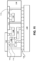
- FIG. 11 illustrates an interposer 1100 that includes one or more embodiments of the disclosure.
- the interposer 1100 is an intervening substrate used to bridge a first substrate 1102 to a second substrate 1104 .
- the first substrate 1102 may be, for instance, an integrated circuit die.
- the second substrate 1104 may be, for instance, a memory module, a computer motherboard, or another integrated circuit die.
- the purpose of an interposer 1100 is to spread a connection to a wider pitch or to reroute a connection to a different connection.
- an interposer 1100 may couple an integrated circuit die to a ball grid array (BGA) 1106 that can subsequently be coupled to the second substrate 1104 .
- BGA ball grid array
- first and second substrates 1102 / 1104 are attached to opposing sides of the interposer 1100 . In other embodiments, the first and second substrates 1102 / 1104 are attached to the same side of the interposer 1100 . And in further embodiments, three or more substrates are interconnected by way of the interposer 1100 .
- the interposer 1100 may be formed of an epoxy resin, a fiberglass-reinforced epoxy resin, a ceramic material, or a polymer material such as polyimide.
- the interposer may be formed of alternate rigid or flexible materials that may include the same materials described above for use in a semiconductor substrate, such as silicon, germanium, and other group III-V and group IV materials.
- the interposer may include metal interconnects 1108 and vias 1110 , including but not limited to through-silicon vias (TSVs) 1112 .
- the interposer 1100 may further include embedded devices 1114 , including both passive and active devices. Such devices include, but are not limited to, capacitors, decoupling capacitors, resistors, inductors, fuses, diodes, transformers, sensors, and electrostatic discharge (ESD) devices. More complex devices such as radio-frequency (RF) devices, power amplifiers, power management devices, antennas, arrays, sensors, and MEMS devices may also be formed on the interposer 1100 .
- RF radio-frequency
- apparatuses or processes disclosed herein may be used in the fabrication of interposer 1100 .
- embodiments of the present disclosure include carbon-based dielectric materials for semiconductor structure fabrication, and the resulting structures.
- a method of patterning a layer for a semiconductor structure includes forming a plurality of trenches in a dielectric layer above a semiconductor layer above a substrate to form a patterned dielectric layer. The method also includes filling the plurality of trenches with an adamantane-based carbon hardmask material. The method also includes removing the patterned dielectric layer selective to the adamantane-based carbon hardmask material. The method also includes using the adamantane-based carbon hardmask material to pattern the semiconductor layer.
- filling the plurality of trenches with the adamantane-based carbon hardmask material includes using a spin-on deposition process or a flowable chemical vapor deposition process.
- the method of example embodiment 1, 2 or 3 wherein using the adamantane-based carbon hardmask material to pattern the semiconductor layer includes forming a plurality of semiconductor fins in the semiconductor layer.
- An integrated circuit structure includes a gate stack above a substrate.
- a first and a second conductive trench contact are at first and second sides of the gate stack, respectively.
- a first hardmask component is on and aligned with an uppermost surface of the gate stack.
- a second hardmask component is on and aligned with first and second conductive trench contacts.
- the first and second hardmask components differ in composition from one another.
- One of the first hardmask component or the second hardmask component includes an adamantane-based carbon hardmask material.
- a conductive via is in an opening in the first hardmask component and on a portion of the gate stack.
- An integrated circuit structure includes an inter-layer dielectric (ILD) layer above a substrate.
- ILD inter-layer dielectric
- a conductive interconnect line is in a trench in the ILD layer, the conductive interconnect line having a first portion and a second portion, the first portion laterally adjacent to the second portion.
- a dielectric plug is between and laterally adjacent to the first and second portions of the conductive interconnect line, the dielectric plug including an adamantane-based carbon hardmask material.
- the integrated circuit structure of example embodiment 9, 10, 11, 12 or 13, further including a first conductive via in a second trench in the ILD layer, the first conductive via below the bottom of the interconnect line, and the first conductive via electrically coupled to the first portion of the conductive interconnect line, and a second conductive via in a third trench in the ILD layer, the second conductive via below the bottom of the interconnect line, and the second conductive via electrically coupled to the second portion of the conductive interconnect line.
- the conductive interconnect line includes a conductive barrier liner and a conductive fill material, the conductive fill material including cobalt.
- An interconnect structure for an integrated circuit includes a first layer of the interconnect structure disposed above a substrate.
- the first layer includes a first grating of alternating metal lines and dielectric lines in a first direction.
- the dielectric lines have an uppermost surface higher than an uppermost surface of the metal lines.
- a second layer of the interconnect structure is disposed above the first layer of the interconnect structure.
- the second layer includes a second grating of alternating metal lines and dielectric lines in a second direction, perpendicular to the first direction.
- the dielectric lines have a lowermost surface lower than a lowermost surface of the metal lines of the second grating.
- the dielectric lines of the second grating overlap and contact, but are distinct from, the dielectric lines of the first grating.
- a region of dielectric material is disposed between the metal lines of the first grating and the metal lines of the second grating, and in a same plane as upper portions of the dielectric lines of the first grating and lower portions of the dielectric lines of the second grating.
- the region of dielectric material includes an adamantane-based carbon hardmask material.
- interconnect structure of example embodiment 16 further including a conductive via disposed between and coupling a metal line of the first grating to a metal line of the second grating.
- the interconnect structure of example embodiment 19, and the dielectric lines of the second grating are composed of a second, different dielectric material.
- the first and second dielectric materials are different than the region of dielectric material composed of the adamantane-based carbon hardmask material.
Landscapes
- Chemical & Material Sciences (AREA)
- Inorganic Chemistry (AREA)
- General Chemical & Material Sciences (AREA)
- Chemical Kinetics & Catalysis (AREA)
- Engineering & Computer Science (AREA)
- Materials Engineering (AREA)
- Mechanical Engineering (AREA)
- Metallurgy (AREA)
- Organic Chemistry (AREA)
- Internal Circuitry In Semiconductor Integrated Circuit Devices (AREA)
- Drying Of Semiconductors (AREA)
Abstract
Description
Claims (20)
Applications Claiming Priority (1)
| Application Number | Priority Date | Filing Date | Title |
|---|---|---|---|
| PCT/US2018/024771 WO2019190495A1 (en) | 2018-03-28 | 2018-03-28 | Carbon-based dielectric materials for semiconductor structure fabrication and the resulting structures |
Publications (2)
| Publication Number | Publication Date |
|---|---|
| US20210057230A1 US20210057230A1 (en) | 2021-02-25 |
| US11217455B2 true US11217455B2 (en) | 2022-01-04 |
Family
ID=68060374
Family Applications (1)
| Application Number | Title | Priority Date | Filing Date |
|---|---|---|---|
| US16/954,419 Expired - Fee Related US11217455B2 (en) | 2018-03-28 | 2018-03-28 | Carbon-based dielectric materials for semiconductor structure fabrication and the resulting structures |
Country Status (4)
| Country | Link |
|---|---|
| US (1) | US11217455B2 (en) |
| EP (1) | EP3776644A1 (en) |
| JP (1) | JP7151976B2 (en) |
| WO (1) | WO2019190495A1 (en) |
Families Citing this family (3)
| Publication number | Priority date | Publication date | Assignee | Title |
|---|---|---|---|---|
| US11393754B2 (en) * | 2018-09-28 | 2022-07-19 | Intel Corporation | Contact over active gate structures with etch stop layers for advanced integrated circuit structure fabrication |
| US11862559B2 (en) | 2020-07-31 | 2024-01-02 | Taiwan Semiconductor Manufacturing Co., Ltd. | Semiconductor structures and methods of forming the same |
| US12260296B1 (en) | 2020-12-16 | 2025-03-25 | Intel Corporation | Diamondoid materials in quantum computing devices |
Citations (6)
| Publication number | Priority date | Publication date | Assignee | Title |
|---|---|---|---|---|
| US20070057253A1 (en) * | 2005-08-29 | 2007-03-15 | Rohm And Haas Electronic Materials Llc | Antireflective hard mask compositions |
| US20080009647A1 (en) | 2004-09-24 | 2008-01-10 | Idemitsu Kosan Co., Ltd. | Adamantane Derivative, Process for Producing the Same, and Photosensitive Material for Photoresist |
| US20090163035A1 (en) | 2005-03-08 | 2009-06-25 | Lam Research Corporation | Etch with high etch rate resist mask |
| JP2010156985A (en) | 2010-02-03 | 2010-07-15 | Panasonic Corp | Material for forming barrier film and pattern forming method using same |
| US20140094035A1 (en) | 2012-05-18 | 2014-04-03 | Novellus Systems, Inc. | Carbon deposition-etch-ash gap fill process |
| KR20160146881A (en) | 2014-06-13 | 2016-12-21 | 후지필름 가부시키가이샤 | Pattern forming method, active light sensitive or radiation sensitive resin composition, active light sensitive or radiation sensitive film, method for manufacturing electronic device, and electronic device |
Family Cites Families (3)
| Publication number | Priority date | Publication date | Assignee | Title |
|---|---|---|---|---|
| JP2003252982A (en) | 2002-03-06 | 2003-09-10 | Fujitsu Ltd | Organic insulating film material, manufacturing method thereof, method of forming organic insulating film, and semiconductor device provided with organic insulating film |
| JP4335932B2 (en) | 2007-02-27 | 2009-09-30 | 富士通株式会社 | Semiconductor device manufacturing and manufacturing method thereof |
| EP3559746B1 (en) | 2016-12-21 | 2021-03-31 | Merck Patent GmbH | Composition of spin-on materials containing metal oxide nanoparticles and an organic polymer |
-
2018
- 2018-03-28 EP EP18912552.9A patent/EP3776644A1/en not_active Withdrawn
- 2018-03-28 JP JP2020533231A patent/JP7151976B2/en active Active
- 2018-03-28 WO PCT/US2018/024771 patent/WO2019190495A1/en not_active Ceased
- 2018-03-28 US US16/954,419 patent/US11217455B2/en not_active Expired - Fee Related
Patent Citations (7)
| Publication number | Priority date | Publication date | Assignee | Title |
|---|---|---|---|---|
| US20080009647A1 (en) | 2004-09-24 | 2008-01-10 | Idemitsu Kosan Co., Ltd. | Adamantane Derivative, Process for Producing the Same, and Photosensitive Material for Photoresist |
| US20090163035A1 (en) | 2005-03-08 | 2009-06-25 | Lam Research Corporation | Etch with high etch rate resist mask |
| US20070057253A1 (en) * | 2005-08-29 | 2007-03-15 | Rohm And Haas Electronic Materials Llc | Antireflective hard mask compositions |
| JP2010156985A (en) | 2010-02-03 | 2010-07-15 | Panasonic Corp | Material for forming barrier film and pattern forming method using same |
| US20140094035A1 (en) | 2012-05-18 | 2014-04-03 | Novellus Systems, Inc. | Carbon deposition-etch-ash gap fill process |
| KR20160146881A (en) | 2014-06-13 | 2016-12-21 | 후지필름 가부시키가이샤 | Pattern forming method, active light sensitive or radiation sensitive resin composition, active light sensitive or radiation sensitive film, method for manufacturing electronic device, and electronic device |
| US20170059995A1 (en) | 2014-06-13 | 2017-03-02 | Fujifilm Corporation | Pattern forming method, active light sensitive or radiation sensitive resin composition, active light sensitive or radiation sensitive film, method for manufacturing electronic device, and electronic device |
Non-Patent Citations (2)
| Title |
|---|
| International Preliminary Report on Patentability for International Patent Application No. PCT/US2018/024771, dated Oct. 8, 2020, 7 pgs. |
| International Search Report and Written Opinion for International Patent Application No. PCT/US2018/024771 dated Dec. 18, 2018, 11 pgs. |
Also Published As
| Publication number | Publication date |
|---|---|
| JP2021524996A (en) | 2021-09-16 |
| EP3776644A1 (en) | 2021-02-17 |
| WO2019190495A1 (en) | 2019-10-03 |
| JP7151976B2 (en) | 2022-10-12 |
| US20210057230A1 (en) | 2021-02-25 |
Similar Documents
| Publication | Publication Date | Title |
|---|---|---|
| US11990403B2 (en) | Dielectric helmet-based approaches for back end of line (BEOL) interconnect fabrication and structures resulting therefrom | |
| US10636700B2 (en) | Metal via processing schemes with via critical dimension (CD) control for back end of line (BEOL) interconnects and the resulting structures | |
| US12341061B2 (en) | Bottom-up fill dielectric materials for semiconductor structure fabrication and their methods of fabrication | |
| US11373900B2 (en) | Damascene plug and tab patterning with photobuckets | |
| US10559529B2 (en) | Pitch division patterning approaches with increased overlay margin for back end of line (BEOL) interconnect fabrication and structures resulting therefrom | |
| US10522402B2 (en) | Grid self-aligned metal via processing schemes for back end of line (BEOL) interconnects and structures resulting therefrom | |
| US10770291B2 (en) | Methods and masks for line end formation for back end of line (BEOL) interconnects and structures resulting therefrom | |
| US11145541B2 (en) | Conductive via and metal line end fabrication and structures resulting therefrom | |
| WO2019190453A1 (en) | Selective etching and controlled atomic layer etching of transition metal oxide films for device fabrication | |
| US11710636B2 (en) | Metal and spacer patterning for pitch division with multiple line widths and spaces | |
| US11217455B2 (en) | Carbon-based dielectric materials for semiconductor structure fabrication and the resulting structures | |
| WO2018236354A1 (en) | Metal spacer-based approaches for conductive interconnect and via fabrication and structures resulting therefrom | |
| US10529660B2 (en) | Pore-filled dielectric materials for semiconductor structure fabrication and their methods of fabrication | |
| US11894270B2 (en) | Grating replication using helmets and topographically-selective deposition | |
| CN109952637A (en) | Surface for last part technology (BEOL) interconnection manufacture is directed at lithographic patterning mode | |
| US11367684B2 (en) | Recessed metal interconnects to mitigate EPE-related via shorting |
Legal Events
| Date | Code | Title | Description |
|---|---|---|---|
| FEPP | Fee payment procedure |
Free format text: ENTITY STATUS SET TO UNDISCOUNTED (ORIGINAL EVENT CODE: BIG.); ENTITY STATUS OF PATENT OWNER: LARGE ENTITY |
|
| STPP | Information on status: patent application and granting procedure in general |
Free format text: APPLICATION DISPATCHED FROM PREEXAM, NOT YET DOCKETED |
|
| STPP | Information on status: patent application and granting procedure in general |
Free format text: DOCKETED NEW CASE - READY FOR EXAMINATION |
|
| STPP | Information on status: patent application and granting procedure in general |
Free format text: NOTICE OF ALLOWANCE MAILED -- APPLICATION RECEIVED IN OFFICE OF PUBLICATIONS |
|
| AS | Assignment |
Owner name: INTEL CORPORATION, CALIFORNIA Free format text: ASSIGNMENT OF ASSIGNORS INTEREST;ASSIGNORS:BLACKWELL, JAMES M.;MAHDI, TAYSEER;REEL/FRAME:057999/0644 Effective date: 20180418 |
|
| STPP | Information on status: patent application and granting procedure in general |
Free format text: PUBLICATIONS -- ISSUE FEE PAYMENT VERIFIED |
|
| STCF | Information on status: patent grant |
Free format text: PATENTED CASE |
|
| FEPP | Fee payment procedure |
Free format text: MAINTENANCE FEE REMINDER MAILED (ORIGINAL EVENT CODE: REM.); ENTITY STATUS OF PATENT OWNER: LARGE ENTITY |
|
| LAPS | Lapse for failure to pay maintenance fees |
Free format text: PATENT EXPIRED FOR FAILURE TO PAY MAINTENANCE FEES (ORIGINAL EVENT CODE: EXP.); ENTITY STATUS OF PATENT OWNER: LARGE ENTITY |
|
| STCH | Information on status: patent discontinuation |
Free format text: PATENT EXPIRED DUE TO NONPAYMENT OF MAINTENANCE FEES UNDER 37 CFR 1.362 |
|
| FP | Lapsed due to failure to pay maintenance fee |
Effective date: 20260104 |