US11216634B2 - Ultrasonic sensor and display device - Google Patents
Ultrasonic sensor and display device Download PDFInfo
- Publication number
- US11216634B2 US11216634B2 US17/107,746 US202017107746A US11216634B2 US 11216634 B2 US11216634 B2 US 11216634B2 US 202017107746 A US202017107746 A US 202017107746A US 11216634 B2 US11216634 B2 US 11216634B2
- Authority
- US
- United States
- Prior art keywords
- sensing
- electrode
- period
- voltage
- supplied
- Prior art date
- Legal status (The legal status is an assumption and is not a legal conclusion. Google has not performed a legal analysis and makes no representation as to the accuracy of the status listed.)
- Active
Links
Images


Classifications
-
- G—PHYSICS
- G01—MEASURING; TESTING
- G01H—MEASUREMENT OF MECHANICAL VIBRATIONS OR ULTRASONIC, SONIC OR INFRASONIC WAVES
- G01H11/00—Measuring mechanical vibrations or ultrasonic, sonic or infrasonic waves by detecting changes in electric or magnetic properties
- G01H11/06—Measuring mechanical vibrations or ultrasonic, sonic or infrasonic waves by detecting changes in electric or magnetic properties by electric means
- G01H11/08—Measuring mechanical vibrations or ultrasonic, sonic or infrasonic waves by detecting changes in electric or magnetic properties by electric means using piezoelectric devices
-
- G—PHYSICS
- G01—MEASURING; TESTING
- G01S—RADIO DIRECTION-FINDING; RADIO NAVIGATION; DETERMINING DISTANCE OR VELOCITY BY USE OF RADIO WAVES; LOCATING OR PRESENCE-DETECTING BY USE OF THE REFLECTION OR RERADIATION OF RADIO WAVES; ANALOGOUS ARRANGEMENTS USING OTHER WAVES
- G01S15/00—Systems using the reflection or reradiation of acoustic waves, e.g. sonar systems
- G01S15/88—Sonar systems specially adapted for specific applications
- G01S15/89—Sonar systems specially adapted for specific applications for mapping or imaging
-
- G06K9/0002—
-
- B—PERFORMING OPERATIONS; TRANSPORTING
- B06—GENERATING OR TRANSMITTING MECHANICAL VIBRATIONS IN GENERAL
- B06B—METHODS OR APPARATUS FOR GENERATING OR TRANSMITTING MECHANICAL VIBRATIONS OF INFRASONIC, SONIC, OR ULTRASONIC FREQUENCY, e.g. FOR PERFORMING MECHANICAL WORK IN GENERAL
- B06B1/00—Methods or apparatus for generating mechanical vibrations of infrasonic, sonic, or ultrasonic frequency
- B06B1/02—Methods or apparatus for generating mechanical vibrations of infrasonic, sonic, or ultrasonic frequency making use of electrical energy
- B06B1/06—Methods or apparatus for generating mechanical vibrations of infrasonic, sonic, or ultrasonic frequency making use of electrical energy operating with piezoelectric effect or with electrostriction
- B06B1/0644—Methods or apparatus for generating mechanical vibrations of infrasonic, sonic, or ultrasonic frequency making use of electrical energy operating with piezoelectric effect or with electrostriction using a single piezoelectric element
- B06B1/0662—Methods or apparatus for generating mechanical vibrations of infrasonic, sonic, or ultrasonic frequency making use of electrical energy operating with piezoelectric effect or with electrostriction using a single piezoelectric element with an electrode on the sensitive surface
-
- B—PERFORMING OPERATIONS; TRANSPORTING
- B06—GENERATING OR TRANSMITTING MECHANICAL VIBRATIONS IN GENERAL
- B06B—METHODS OR APPARATUS FOR GENERATING OR TRANSMITTING MECHANICAL VIBRATIONS OF INFRASONIC, SONIC, OR ULTRASONIC FREQUENCY, e.g. FOR PERFORMING MECHANICAL WORK IN GENERAL
- B06B1/00—Methods or apparatus for generating mechanical vibrations of infrasonic, sonic, or ultrasonic frequency
- B06B1/02—Methods or apparatus for generating mechanical vibrations of infrasonic, sonic, or ultrasonic frequency making use of electrical energy
- B06B1/0207—Driving circuits
- B06B1/0215—Driving circuits for generating pulses, e.g. bursts of oscillations, envelopes
-
- B—PERFORMING OPERATIONS; TRANSPORTING
- B06—GENERATING OR TRANSMITTING MECHANICAL VIBRATIONS IN GENERAL
- B06B—METHODS OR APPARATUS FOR GENERATING OR TRANSMITTING MECHANICAL VIBRATIONS OF INFRASONIC, SONIC, OR ULTRASONIC FREQUENCY, e.g. FOR PERFORMING MECHANICAL WORK IN GENERAL
- B06B1/00—Methods or apparatus for generating mechanical vibrations of infrasonic, sonic, or ultrasonic frequency
- B06B1/02—Methods or apparatus for generating mechanical vibrations of infrasonic, sonic, or ultrasonic frequency making use of electrical energy
- B06B1/06—Methods or apparatus for generating mechanical vibrations of infrasonic, sonic, or ultrasonic frequency making use of electrical energy operating with piezoelectric effect or with electrostriction
- B06B1/0688—Methods or apparatus for generating mechanical vibrations of infrasonic, sonic, or ultrasonic frequency making use of electrical energy operating with piezoelectric effect or with electrostriction with foil-type piezoelectric elements, e.g. PVDF
- B06B1/0692—Methods or apparatus for generating mechanical vibrations of infrasonic, sonic, or ultrasonic frequency making use of electrical energy operating with piezoelectric effect or with electrostriction with foil-type piezoelectric elements, e.g. PVDF with a continuous electrode on one side and a plurality of electrodes on the other side
-
- G—PHYSICS
- G06—COMPUTING OR CALCULATING; COUNTING
- G06F—ELECTRIC DIGITAL DATA PROCESSING
- G06F3/00—Input arrangements for transferring data to be processed into a form capable of being handled by the computer; Output arrangements for transferring data from processing unit to output unit, e.g. interface arrangements
- G06F3/01—Input arrangements or combined input and output arrangements for interaction between user and computer
- G06F3/03—Arrangements for converting the position or the displacement of a member into a coded form
- G06F3/041—Digitisers, e.g. for touch screens or touch pads, characterised by the transducing means
- G06F3/0414—Digitisers, e.g. for touch screens or touch pads, characterised by the transducing means using force sensing means to determine a position
-
- G—PHYSICS
- G06—COMPUTING OR CALCULATING; COUNTING
- G06F—ELECTRIC DIGITAL DATA PROCESSING
- G06F3/00—Input arrangements for transferring data to be processed into a form capable of being handled by the computer; Output arrangements for transferring data from processing unit to output unit, e.g. interface arrangements
- G06F3/01—Input arrangements or combined input and output arrangements for interaction between user and computer
- G06F3/03—Arrangements for converting the position or the displacement of a member into a coded form
- G06F3/041—Digitisers, e.g. for touch screens or touch pads, characterised by the transducing means
- G06F3/043—Digitisers, e.g. for touch screens or touch pads, characterised by the transducing means using propagating acoustic waves
-
- G06K9/209—
-
- G—PHYSICS
- G06—COMPUTING OR CALCULATING; COUNTING
- G06V—IMAGE OR VIDEO RECOGNITION OR UNDERSTANDING
- G06V40/00—Recognition of biometric, human-related or animal-related patterns in image or video data
- G06V40/10—Human or animal bodies, e.g. vehicle occupants or pedestrians; Body parts, e.g. hands
- G06V40/12—Fingerprints or palmprints
- G06V40/13—Sensors therefor
- G06V40/1306—Sensors therefor non-optical, e.g. ultrasonic or capacitive sensing
-
- H—ELECTRICITY
- H10—SEMICONDUCTOR DEVICES; ELECTRIC SOLID-STATE DEVICES NOT OTHERWISE PROVIDED FOR
- H10N—ELECTRIC SOLID-STATE DEVICES NOT OTHERWISE PROVIDED FOR
- H10N30/00—Piezoelectric or electrostrictive devices
- H10N30/20—Piezoelectric or electrostrictive devices with electrical input and mechanical output, e.g. functioning as actuators or vibrators
-
- H—ELECTRICITY
- H10—SEMICONDUCTOR DEVICES; ELECTRIC SOLID-STATE DEVICES NOT OTHERWISE PROVIDED FOR
- H10N—ELECTRIC SOLID-STATE DEVICES NOT OTHERWISE PROVIDED FOR
- H10N30/00—Piezoelectric or electrostrictive devices
- H10N30/80—Constructional details
- H10N30/802—Circuitry or processes for operating piezoelectric or electrostrictive devices not otherwise provided for, e.g. drive circuits
-
- H—ELECTRICITY
- H10—SEMICONDUCTOR DEVICES; ELECTRIC SOLID-STATE DEVICES NOT OTHERWISE PROVIDED FOR
- H10N—ELECTRIC SOLID-STATE DEVICES NOT OTHERWISE PROVIDED FOR
- H10N30/00—Piezoelectric or electrostrictive devices
- H10N30/80—Constructional details
- H10N30/85—Piezoelectric or electrostrictive active materials
- H10N30/853—Ceramic compositions
-
- H—ELECTRICITY
- H10—SEMICONDUCTOR DEVICES; ELECTRIC SOLID-STATE DEVICES NOT OTHERWISE PROVIDED FOR
- H10N—ELECTRIC SOLID-STATE DEVICES NOT OTHERWISE PROVIDED FOR
- H10N30/00—Piezoelectric or electrostrictive devices
- H10N30/80—Constructional details
- H10N30/87—Electrodes or interconnections, e.g. leads or terminals
-
- B—PERFORMING OPERATIONS; TRANSPORTING
- B06—GENERATING OR TRANSMITTING MECHANICAL VIBRATIONS IN GENERAL
- B06B—METHODS OR APPARATUS FOR GENERATING OR TRANSMITTING MECHANICAL VIBRATIONS OF INFRASONIC, SONIC, OR ULTRASONIC FREQUENCY, e.g. FOR PERFORMING MECHANICAL WORK IN GENERAL
- B06B2201/00—Indexing scheme associated with B06B1/0207 for details covered by B06B1/0207 but not provided for in any of its subgroups
- B06B2201/50—Application to a particular transducer type
- B06B2201/55—Piezoelectric transducer
- B06B2201/56—Foil type, e.g. PVDF
-
- B—PERFORMING OPERATIONS; TRANSPORTING
- B06—GENERATING OR TRANSMITTING MECHANICAL VIBRATIONS IN GENERAL
- B06B—METHODS OR APPARATUS FOR GENERATING OR TRANSMITTING MECHANICAL VIBRATIONS OF INFRASONIC, SONIC, OR ULTRASONIC FREQUENCY, e.g. FOR PERFORMING MECHANICAL WORK IN GENERAL
- B06B2201/00—Indexing scheme associated with B06B1/0207 for details covered by B06B1/0207 but not provided for in any of its subgroups
- B06B2201/70—Specific application
-
- G06K9/0008—
-
- G—PHYSICS
- G06—COMPUTING OR CALCULATING; COUNTING
- G06V—IMAGE OR VIDEO RECOGNITION OR UNDERSTANDING
- G06V40/00—Recognition of biometric, human-related or animal-related patterns in image or video data
- G06V40/10—Human or animal bodies, e.g. vehicle occupants or pedestrians; Body parts, e.g. hands
- G06V40/12—Fingerprints or palmprints
- G06V40/1347—Preprocessing; Feature extraction
- G06V40/1359—Extracting features related to ridge properties; Determining the fingerprint type, e.g. whorl or loop
Definitions
- Embodiments of the disclosure are related to ultrasonic sensors and display devices.
- the display device for providing more various functions to a user, recognizes a touch of the user to a display panel, or recognizes a biometric data (e.g., a fingerprint or the like) or a gesture that is in contact with or close to the display panel, and provides a function performing an input process based on the recognized information.
- a biometric data e.g., a fingerprint or the like
- a gesture that is in contact with or close to the display panel
- an optical sensor or the like may be used to recognize the biometric data or the like. But in a case that the optical sensor or the like is disposed in a bezel area of the display panel, there is a problem that an active area is reduced. Furthermore, in a case that the optical sensor is disposed in the active area, there is a problem to affect a display driving or reduce an accuracy of a sensing.
- a method is necessary to improve a sensing performance of the biometric data or the like in the active area of the display panel without affecting the display driving of the display panel.
- embodiments of the present disclosure are directed to an ultrasonic sensor and a display device that substantially obviate one or more of the problems due to limitations and disadvantages of the related art.
- An aspect of the present disclosure is to provide a function performing a sensing a biometric data or the like in an active area of a display panel, and a method improving a sensing performance of the biometric data or the like.
- Another aspect of the present disclosure is to provide a method increasing a sensing efficiency and a sensing accuracy while minimizing a falling of the sensing performance due to a deterioration of a sensor for sensing the biometric data or the like.
- an ultrasonic sensor may comprise a pixel array which a plurality of scan lines, a plurality of sensing lines and a plurality of sensing pixels are disposed, a plurality of first electrode disposed in each of the plurality of sensing pixels, a piezoelectric material disposed on the first electrode, and a second electrode disposed on the piezoelectric material.
- a first driving voltage may be simultaneously supplied to the plurality of first electrodes in a first period, and a second driving voltage may be supplied to the second electrode in the first period.
- a supply of the first driving voltage to the first electrode is stopped at a preset timing in the second period, and a sensing signal may be detected from the sensing pixel in a third period.
- an ultrasonic sensor may comprise a pixel array which a plurality of scan lines, a plurality of sensing lines and a plurality of sensing pixels are disposed, a plurality of first electrodes disposed in each of the plurality of sensing pixels, a piezoelectric material disposed on the first electrode, and a second electrode disposed on the piezoelectric material, wherein a second driving voltage is supplied to the second electrode in a part of a period that a first driving voltage is simultaneously supplied to the plurality of first electrodes, and then a sensing signal is detected from the plurality of sensing pixels, and a period that the plurality of first electrodes are in a floating state is present between a period that the second driving voltage is supplied and a period that the sensing signal is detected.
- a display device may comprise a display panel, and above-mentioned ultrasonic sensor embedded in the display panel or disposed on at least one surface of the display panel.
- a sensing function of the biometric data or the like in an active area may be provided while preventing a reduction of the active area of the display panel.
- an accuracy of a sensing may be improved while increasing a driving efficiency of the ultrasonic sensor.
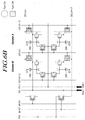
- FIG. 1 is a view schematically illustrating a configuration of an ultrasonic sensor according to various embodiments of the disclosure
- FIG. 2 is a view illustrating an example of a circuit structure of a pixel array of the ultrasonic sensor according to various embodiments of the disclosure
- FIG. 3 is a view illustrating an example of a driving method of the ultrasonic sensor according to various embodiments of the disclosure
- FIG. 4 is a view illustrating an example of a supplied signal and a timing that the signal is supplied when driving the ultrasonic sensor according to various embodiments of the disclosure
- FIG. 5 is a view illustrating an example of a method driving a sensing pixel disposed in the ultrasonic sensor according to various embodiments of the disclosure in an ultrasonic wave transmitting period;
- FIGS. 6A and 6B are views illustrating an example of a method driving the sensing pixel disposed in the ultrasonic sensor according to various embodiments of the disclosure in an ultrasonic wave receiving period;
- FIGS. 7A, 7B, 7C and 7D are views illustrating an example of a method driving the sensing pixel disposed in the ultrasonic sensor according to various embodiments of the disclosure in a readout period;
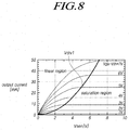
- FIG. 8 is a view illustrating an example of a relation between a sensing voltage and a sensing signal according a voltage supplied to a receiving electrode in the ultrasonic sensor according to various embodiments of the disclosure.
- FIG. 9 is a view illustrating another example of a supplied signal and a timing that the signal is supplied when driving the ultrasonic sensor according to various embodiments of the disclosure.
- first element is connected or coupled to”, “contacts or overlaps” etc. a second element
- first element is connected or coupled to” or “directly contact or overlap” the second element
- a third element can also be “interposed” between the first and second elements, or the first and second elements can “be connected or coupled to”, “contact or overlap”, etc. each other via a fourth element.
- the second element may be included in at least one of two or more elements that “are connected or coupled to”, “contact or overlap”, etc. each other.
- time relative terms such as “after,” “subsequent to,” “next,” “before,” and the like, are used to describe processes or operations of elements or configurations, or flows or steps in operating, processing, manufacturing methods, these terms may be used to describe non-consecutive or non-sequential processes or operations unless the term “directly” or “immediately” is used together.
- FIG. 1 is a view schematically illustrating a configuration of an ultrasonic sensor 200 according to various embodiments of the disclosure, and FIG. 1 illustrates an example of a structure that the ultrasonic sensor 200 is disposed on a display device.
- the display device may comprise a display panel 110 in which a plurality of gate lines, a plurality of data lines and a plurality of subpixels are disposed, and various driving circuits to drive a signal line or a voltage line disposed on the display panel 110 .
- the ultrasonic sensor 200 or an ultrasonic wave sensing device to sense a biometric data e.g., a fingerprint
- a biometric data e.g., a fingerprint
- a gesture that is in contact with or close to the display panel 110
- this ultrasonic sensor 200 may be disposed inside the display device as an embedded type.
- a cover glass 120 may be disposed on a side that an image is displayed in the display panel 110 .
- the ultrasonic sensor 200 may be disposed on an opposite side of the side that the image is displayed in the display panel 110 . That is, the ultrasonic sensor 200 may be disposed on an opposite side of a side that the cover glass 120 is disposed.
- This ultrasonic sensor 200 may be bonded to the display panel 110 by an adhesive portion 300 .
- the adhesive portion 300 may be made of a resin.
- the ultrasonic sensor 200 may generate an ultrasonic wave, sense a reflected ultrasonic wave from a fingerprint contacted to the cover glass 120 disposed on the display panel 110 , and recognize the fingerprint contacted to the cover glass 120 . As the ultrasonic sensor 200 performs a sensing being disposed on an opposite side of a side that an image is displayed in the display panel 110 , a fingerprint sensing may be possible without reducing an area that the image is displayed.
- the ultrasonic wave generated from the ultrasonic sensor 200 when the ultrasonic wave generated from the ultrasonic sensor 200 is reached to a valley portion of the fingerprint, the ultrasonic wave may reach an air that is present between a skin of a people and the cover glass 120 .
- most of the ultrasonic wave reached to the air may be reflected due to a difference of an acoustic impedance value between the cover glass 120 and the air.
- the ultrasonic wave generated from the ultrasonic sensor 200 may reach the skin of the people contacted to the cover glass 120 .
- a part of the ultrasonic wave may be reflected, but most of the ultrasonic wave may be transmitted inside the skin and may be reflected inside the skin.
- the fingerprint may be sensed by separating the valley portion and the ridge portion of the fingerprint.
- the ultrasonic sensor 200 may provide merits of not sensitive of a contamination or a condition of a skin surface and an excellent security, since the ultrasonic sensor 200 sense inside the skin. Furthermore, the display device may perform an input process using the fingerprint sensed, as sensing the fingerprint without reducing an area that the image is displayed.
- This ultrasonic sensor 200 may comprise a material for generating the ultrasonic wave, and various circuit elements for generating and sensing the ultrasonic wave.
- the ultrasonic sensor 200 may comprise a substrate 210 , a thin film transistor array 220 disposed on the substrate 210 , a first pad portion 231 , a second pad portion 232 .
- the thin film transistor array 220 may comprise a first electrode E 1 disposed in each pixel, and a piezoelectric material 240 and a second electrode E 2 may be disposed on the thin film transistor array 220 sequentially.
- the first electrode E 1 may be regarded as a pixel electrode, and the second electrode E 1 may be regarded as a common electrode. And one of the first electrode E 1 and the second electrode E 2 may be a transmitting electrode, and the other may be a receiving electrode.
- the piezoelectric material 240 may be a material of PZT, ZnO, perovskite or the like, but not limited to these.
- the second electrode E 2 may be bonded to a reflection layer 260 by an adhesive layer 250 , and a cover layer 270 may be disposed on the reflection layer 260 .
- a controller 400 supplying a signal, a voltage or the like to the thin film transistor array 220 and the second electrode E 2 or the like may be electrically connected to the second pad portion 232 disposed on the substrate 210 through a flexible printed circuit 290 and a bonding portion 280 .
- a transistor for driving of generating the ultrasonic wave and sensing of the ultrasonic wave reflected from the fingerprint, and the first electrode E 1 may be disposed.
- the first electrode E 1 disposed in the thin film transistor array 220 may be formed as a capacitor with the second electrode E 2 .
- the piezoelectric material 240 may be vibrated and the ultrasonic wave may be generated.
- the thin film transistor array 220 comprising this first electrode E 1 , the piezoelectric material 240 and the second electrode E 2 may be regarded as a pixel array in an aspect of a circuit.
- the second electrode E 2 may be disposed as a method that a silver ink is coated, in some cases, may be disposed as a shape covering whole of the piezoelectric material 240 , or as a certain pattern.
- the reflection layer 260 may be made of a copper, and may perform a function reflecting the ultrasonic wave that is reflected and returned from the fingerprint to the thin film transistor array 220 .
- the cover layer 270 may be made of a polyimide, may provide a function capping the pixel array and the reflection layer 260 or the like of the ultrasonic sensor 200 .
- the reflection layer 260 and the cover layer 270 may be disposed as one film shape, or may be implemented as a shape that an organic material or a dielectric material or the like is coated on the second electrode E 2 .
- the signal and the voltage for driving the pixel array may be supplied from the controller 400 .
- a signal or the like that a high voltage is not required may be supplied from the driving circuit disposed for driving of the display panel 110 .
- FIG. 2 is a view illustrating an example of a circuit structure of the pixel array of the ultrasonic sensor 200 according to various embodiments of the disclosure.
- a plurality of scan lines SCL and a plurality of sensing lines SSL may be disposed.
- the scan line SCL and the sensing line SSL may be disposed crossing each other.
- a plurality of sensing pixels may be disposed in an area defined by the crossing of the scan line SCL and the sensing line SSL.
- a voltage line may be disposed for supplying a driving voltage Vdrv, a sensing voltage Vsen or the like for generating and sensing of the ultrasonic wave of the sensing pixel.
- a first driving voltage line DVL 1 supplying a first driving voltage Vdrv 1 to the first electrode E 1 and a sensing voltage line SVL supplying the sensing voltage Vsen may be disposed.
- the first driving voltage line DVL 1 and the sensing voltage line SVL may be outside of an area where the sensing pixel is disposed.
- a second driving voltage line DVL 2 supplying a second driving voltage Vdrv 2 to the second electrode E 2 may be disposed in the thin film transistor array 220 , or not. That is, the second electrode E 2 may be directly connected to the first pad portion 231 or the like, and may be supplied the second driving voltage Vdrv 2 through the first pad portion 231 .
- the ultrasonic sensor 200 may comprise a circuit to drive the plurality of scan lines SCL disposed in the pixel array, and a circuit or the like to detect a sensing signal through the plurality of sensing lines SSL.
- each sensing pixel various circuit elements may be disposed for generating and sensing the ultrasonic wave.
- a first thin film transistor T 1 and a second thin film transistor T 2 controlled by a scan signal applied to the scan line SCL may be disposed.
- a third thin film transistor T 3 controlled by a voltage level of the first electrode E 1 may be disposed in the sensing pixel.
- a capacitor formed by the first electrode E 1 and the second electrode E 2 may be disposed in the sensing pixel.
- FIG. 2 illustrates a case that a circuit structure of the sensing pixel is 3T1C as an example, the circuit structure of the sensing pixel disposed in the ultrasonic sensor 200 is not limited to this.
- FIG. 2 illustrates a case that all of the first thin film transistor T 1 , the second thin film transistor T 2 and the third thin film transistor T 3 are N types as an example, in some cases, all of those may be implemented as P types.
- the first thin film transistor T 1 and the second thin film transistor T 2 may be implemented as same types, and the third thin film transistor T 3 may be implemented as a different type.
- the first thin film transistor T 1 may be controlled by the scan signal applied to the scan line SCL. And the first thin film transistor T 1 may be electrically connected between the first driving voltage line DVL 1 supplying the first driving voltage Vdrv 1 and the first electrode E 1 .
- the second thin film transistor T 2 may be controlled by the scan signal applied to the scan line SCL. And the second thin film transistor T 2 may be electrically connected between the sensing line SSL and the third thin film transistor T 3 .
- the second thin film transistor T 2 may be driven by a same scan line SCL with the scan line SCL driving the first thin film transistor T 1 disposed in an adjacent sensing pixel.
- all of the second thin film transistor T 2 disposed in the subpixel of a column B and the first thin film transistor T 1 disposed in the subpixel of a column A may be electrically connected to nth scan line SCL(n).
- the first thin film transistor T 1 of the column A and the second thin film transistor T 2 of the column B may be driven simultaneously, the number of the scan line SCL disposed in the pixel array may be reduced.
- the third thin film transistor T 3 may be controlled by the voltage level of the first electrode E 1 . And the third thin film transistor T 3 may be electrically connected between the sensing voltage line SVL and the second thin film transistor T 2 .
- the capacitor formed by the first electrode E 1 and the second electrode E 2 may be disposed.
- the first electrode E 1 may be disposed separately in each sensing pixel, and the second electrode E 2 may be disposed commonly in two or more sensing pixels.
- the piezoelectric material 240 may be disposed between the first electrode E 1 and the second electrode E 2 .
- the piezoelectric material 240 may be vibrated according to the first driving voltage Vdrv 1 supplying to the first electrode E 1 and the second driving voltage Vdrv 2 supplying to the second electrode E 2 , and the ultrasonic wave may be generated.
- one of the first driving voltage Vdrv 1 and the second driving voltage Vdrv 2 may be a constant voltage
- the other for example, may be an alternating current voltage swinging from +100V to ⁇ 100V. That is, as supplying the alternating current voltage to the other electrode in a state that the constant voltage is supplied to one of the first electrode E 1 and the second electrode E 2 , the ultrasonic wave by a vibration of the piezoelectric material 240 may be generated.
- a turn-on state or an output current of the third thin film transistor T 3 may be changed.
- the reflected ultrasonic wave may be sensed and a sensing of the biometric data based on a sensing of the ultrasonic wave may be performed.
- FIG. 3 is a view illustrating an example of a driving method of the ultrasonic sensor 200 according to various embodiments of the disclosure.
- the ultrasonic sensor 200 may be driven by being divided into a sensing period performing a sensing of the ultrasonic wave, and an authentication period performing an information process based on a sensing data acquired in the sensing period.
- the ultrasonic sensor 200 may generate the ultrasonic wave as vibrating the piezoelectric material 240 by driving the first electrode E 1 and the second electrode E 2 disposed in the sensing pixel in a first period P 1 of the sensing period.
- the first period P 1 may be regarded as an ultrasonic wave transmitting period.
- the ultrasonic sensor 200 may transmit the ultrasonic wave by driving all sensing pixel disposed in the pixel array in the ultrasonic wave transmitting period.
- the ultrasonic sensor 200 may receive the reflected ultrasonic wave in a second period P 2 after the first period P 1 , and the second period P 2 may be regarded as an ultrasonic wave receiving period.
- a part of the ultrasonic wave receiving period may be a period to store a received signal.
- the ultrasonic sensor 200 may detect the sensing signal according to the received ultrasonic wave in a third period P 3 after the second period P 2 , and the third period P 3 may be regarded as a readout period.
- a duration for transmitting the ultrasonic wave may be reduced.
- the deterioration of the thin film transistor array 220 due to applying a high voltage may be reduced.
- an accuracy of the sensing may be maintained while reducing the ultrasonic wave transmitting period.
- FIG. 4 is a view illustrating an example of a supplied signal and a timing that the signal is supplied when driving the ultrasonic sensor 200 according to various embodiments of the disclosure.
- FIGS. 5 to 7D are views illustrating examples of a method driving the sensing pixel in a driving process of the ultrasonic sensor 200 .
- FIG. 5 is a view illustrating an example of a method driving the sensing pixel disposed in the ultrasonic sensor 200 according to various embodiments of the disclosure in the ultrasonic wave transmitting period.
- FIGS. 6A and 6B are views illustrating an example of a method driving the sensing pixel disposed in the ultrasonic sensor 200 according to various embodiments of the disclosure in the ultrasonic wave receiving period.
- FIGS. 7A to 7D are views illustrating an example of a method driving the sensing pixel disposed in the ultrasonic sensor 200 according to various embodiments of the disclosure in the readout period.
- the ultrasonic sensor 200 may be driven by being divided into the first period P 1 to transmit the ultrasonic wave, the second period P 2 to receive and store the reflected signal and the third period P 3 to readout the stored signal.
- the driving voltage Vdrv may be supplied to the first electrode E 1 and the second electrode E 2 of the pixel array of the ultrasonic sensor 200 . And according the driving voltage Vdrv, the piezoelectric material 240 disposed between the first electrode E 1 and the second electrode E 2 may be vibrated and the ultrasonic wave may be generated.
- a scan signal of a level to turn on a thin film transistor connected to the scan line SCL may be supplied to the plurality of scan lines SCL.
- all of the first thin film transistor T 1 and the second thin film transistor T 2 connected to the scan line SCL may be turned on.
- the first driving voltage Vdrv 1 supplying through the first driving voltage line DVL 1 may be supplied to the first electrode E 1 disposed in each sensing pixel.
- the second driving voltage Vdrv 2 may be supplied to the second electrode E 2 in a part of a period that the scan signal of a turn on level is supplied to the scan line SCL.
- the first driving voltage Vdrv 1 may be the constant voltage.
- the second driving voltage Vdrv 2 may be the alternating current voltage.
- the second driving voltage Vdrv 2 may be the alternating current voltage swinging by ⁇ based on the first driving voltage Vdrv 1 . If the first driving voltage Vdrv 1 is 10V, the second driving voltage Vdrv 2 may be the alternating current voltage swinging from +110V to ⁇ 90V.
- the ultrasonic wave may be transmitted in all sensing pixels simultaneously.
- a duration and a number of the ultrasonic wave transmitting a period that the high voltage is supplied to the pixel array may be reduced.
- the deterioration of the thin film transistor or the like disposed in the pixel array due to applying the high voltage may be prevented.
- the first driving voltage Vdrv 1 supplied to the first electrode E 1 in the first period P 1 may be a voltage of a level to turn on the third thin film transistor T 3 controlled by the voltage level of the first electrode E 1 .
- the first driving voltage Vdrv 1 may be a lower voltage than a voltage being possible to supply through the first driving voltage line DVL 1 or a maximum voltage Vmax to maximize an output current of the third thin film transistor T 3 .
- a sensing sensitivity may be improved.
- the first driving voltage Vdrv 1 may have the voltage level positioned in a saturation region in a graph representing a relation between the sensing voltage Vsen supplied to the third thin film transistor T 3 and the output current.
- FIG. 8 is a view illustrating an example of a relation between the sensing voltage Vsen and the sensing signal according a voltage supplied to the receiving electrode in the ultrasonic sensor according to various embodiments of the disclosure.
- the voltage level of the first driving voltage Vdrv 1 may be positioned in the saturation region in a relation graph between the sensing voltage Vsen supplied to the third thin film transistor T 3 and the output current of the third thin film transistor T 3 .
- the first driving voltage Vdrv 1 may be configured as 5V positioned in the saturation region. If the voltage level of the first electrode E 1 is increased 1V by the reflected signal to become 6V in a state that a voltage of 5V is applied to the first electrode E 1 , the output current of the third thin film transistor T 3 may be increased 10 mA from about 25 mA to about 35 mA.
- a level of increase of the output current may be greater than a case that the level of the first driving voltage Vdrv 1 is positioned in a linear region
- an intensity of the sensing signal detected through the sensing line SSL may be increased.
- the sensing sensitivity may be improved.
- the level of the first driving voltage Vdrv 1 may be configured to be positioned in the linear area, and the sensing of the ultrasonic wave may be performed.
- a first sensing voltage Vsen 1 may be supplied to a sensing voltage line SVL connected to the third thin film transistor T 3 in the first period P 1 to transmit the ultrasonic wave.
- the first sensing voltage Vsen for example, may be 0V.
- a multiplexer MUX connected to the sensing line SSL may be in a turn off state.
- the sensing line SSL may be initialized by the first sensing voltage Vsen 1 .
- the second electrode E 2 being supplied the second driving voltage Vdrv 2 may become in a floating state. Furthermore, the first electrode E 1 may become in the floating state at a preset timing. That is, a period that the first electrode E 1 is in the floating state may be present between the ultrasonic wave transmitting period and the readout period.
- the sensing pixel in a state maintaining the scan signal of the turn on level in the second period P 2 , a supply of the second driving voltage Vdrv 2 to the second electrode E 2 may be stopped.
- the second electrode E 2 may be in the floating state.
- the sensing pixel may be a state being capable of receiving the reflected signal.
- a supply of the first driving voltage Vdrv 1 to the first electrode E 1 may be stopped according to a timing that the reflected ultrasonic wave is received or the intensity received is the most strongest.
- the first electrode E 1 may become in the floating state according to a peak timing of the received signal.
- the sensing sensitivity may be increased.
- the scan signal of the level to turn off the thin film transistor connected to the scan line SCL may be supplied to the plurality of scan lines SCL at end timing of a delay period P 21 waiting the ultrasonic wave receiving in the second period P 2 .
- the first thin film transistor T 1 become in the turn off state, even if a state that the first driving voltage Vdrv 1 is supplied to the first driving voltage line DVL 1 is maintained, a supply of the first driving voltage Vdrv 1 to the first electrode E 1 may be stopped. And the first electrode E 1 may become in the floating state.
- the received signal may be stored in the first electrode E 1 .
- a state that the first electrode E 1 stores the reflected signal may be maintained during a store period P 22 after supplying the scan signal of the turn off level to the scan line SCL in the second period P 2 .
- the duration of the ultrasonic wave transmitting period may be reduced.
- an accurate sensing may be performed while reducing the ultrasonic wave transmitting period.
- the stored signal may be detected from each sensing pixel sequentially.
- the scan signal of the level to turn on the thin film transistor connected to the scan line SCL may be supplied to (n ⁇ 1)th scan line SCL(n ⁇ 1) in the third period P 3 . And a state that the scan signal of the level to turn off the thin film transistor is supplied to remaining scan lines SCL may be maintained.
- a second sensing voltage Vsen 2 may be supplied to the sensing voltage line SVL.
- the second sensing voltage Vsen 2 may be a higher voltage than the first sensing voltage Vsen 1 being supplied in the first period P 1 and at least a part of the second period P 2 .
- the second thin film transistor T 2 connected to (n ⁇ 1)th scan line SCL(n ⁇ 1) may become in the turn on state all.
- the output current of the third thin film transistor T 3 may be occurred, or a change of the output current may be occurred according to the voltage level of the first electrode E 1 .
- the signal of the level to turn on a first multiplexer MUX 1 may be supplied.
- the stored signal in sensing pixels of the column A connected to mth sensing line SSL(m) may be detected through a readout line ROL.
- the signal of the level to turn on a second multiplexer MUX 2 may be supplied.
- the stored signal in sensing pixels of the column A connected to (m+1)th sensing line SSL(m+1) may be detected through the readout line ROL.
- the stored signal in the first electrode E 1 disposed in each sensing pixel of the column A may be detected sequentially.
- FIGS. 7A and 7B represent an example of four sensing pixels, and for a convenience of an explanation, a structure that two multiplexers MUX and one readout line ROL are disposed is described as an example, a disposition structure of the multiplexer MUX and the readout line ROL is not limited to this.
- the constant voltage may be supplied to the second electrode E 2 in the third period P 3 , for example, a ground voltage may be supplied.
- a reset voltage Vrst different from the first driving voltage Vdrv 1 may be supplied to the first driving voltage line DVL 1 , and the reset voltage Vrst, for example, may be 0V.
- the first electrode E 1 may be reset by the reset voltage Vrst.
- the scan signal of the turn off level may be supplied to (n ⁇ 1)th scan line SCL(n ⁇ 1).
- the second thin film transistor T 2 connected to (n ⁇ 1)th scan line SCL(n ⁇ 1) may become in the turn off state.
- the scan signal of the turn on level may be supplied to nth scan line SCL(n).
- the first thin film transistor T 1 and the second thin film transistor T 2 connected to nth scan line SCL(n) may become in the turn on state.
- the first thin film transistor T 1 disposed in the sensing pixels of the column A and the second thin film transistor T 2 disposed in the sensing pixels of the column B may become in the turn on state.
- (n+1)th scan line SCL(n+1) is a state that the scan signal of the turn off level is supplied, the first thin film transistor T 1 disposed in the sensing pixels of the column B may maintain the turn off state.
- the sensing signal may be detected from the sensing pixels of the column B.
- the first multiplexer MUX 1 may be turned on and the sensing signal stored in the sensing pixels of the column B connected to mth sensing line SSL(m) may be detected through the readout line ROL.
- the second multiplexer MUX 2 may be turned on and the sensing signal stored in the sensing pixels of the column B connected to (m+1)th sensing line SSL(m+1) may be detected through the readout line ROL.
- the reset voltage Vrst being supplied through the first driving voltage line DVL 1 may be supplied to the first electrode E 1 disposed in the sensing pixels of the column A.
- the first electrode E 1 of the sensing pixels of the column A may be reset in a period detecting the sensing signal from the sensing pixels of the column B.
- the ultrasonic wave may be transmitted in the plurality of sensing pixels simultaneously.
- a duration and a number of the ultrasonic wave transmitting may be reduced, the deterioration of the thin film transistor due to applying the high voltage may be prevented.
- only the first electrode E 1 may become in the floating state, and the second electrode E 2 may maintain a constant voltage state after transmitting the ultrasonic wave.
- FIG. 9 is a view illustrating another example of a supplied signal and a timing that the signal is supplied when driving the ultrasonic sensor 200 according to various embodiments of the disclosure.
- the scan signal of the turn on level may be supplied to the plurality of scan lines SCL in the first period P 1 .
- the first driving voltage Vdrv 1 being the constant voltage, may be supplied through the first driving voltage line DVL 1 , the first driving voltage Vdrv 1 may be applied to the first electrode E 1 .
- the second driving voltage Vdrv 2 being the alternating current voltage, may be supplied to the second electrode E 2 in at least a part of a period that the first driving voltage Vdrv 1 is supplied to the first electrode E 1 .
- the piezoelectric material 240 disposed between the first electrode E 1 and the second electrode E 2 may vibrate and the ultrasonic wave may be transmitted.
- a supply of the second driving voltage Vdrv 2 to the second electrode E 2 may be stopped in the second period P 2 .
- the constant voltage may be supplied to the second electrode E 2 , for example, the second electrode E 2 may be a state that the ground voltage is applied.
- the scan signal of the turn off level may be supplied to the plurality of scan lines SCL according to the timing that the reflected signal is received.
- the first electrode E 1 may become in the floating state, and the received signal may be stored in the first electrode E 1 .
- the second electrode E 2 may be maintained as a state that the constant voltage is applied in the third period P 3 , the sensing voltage Vsen being supplied to the sensing voltage line SVL may be changed from the first sensing voltage Vsen 1 to the second sensing voltage Vsen 2 .
- the first electrode E 1 of the sensing pixel which the sensing signal is detected may be reset by the reset voltage Vrst.
- the second electrode E 2 may not be changed to the floating state between the ultrasonic wave transmitting period and the readout period.
- a duration and a number of the ultrasonic wave transmitting may be reduced. Furthermore, by supplying the high voltage for transmitting the ultrasonic wave to the second electrode E 2 disposed on the plurality of sensing pixels commonly, the deterioration of the thin film transistor due to applying the high voltage may be prevented.
- an accuracy of the sensing performed subsequently may be improved without increasing the sensing period.
Landscapes
- Engineering & Computer Science (AREA)
- Physics & Mathematics (AREA)
- Theoretical Computer Science (AREA)
- Mechanical Engineering (AREA)
- General Physics & Mathematics (AREA)
- General Engineering & Computer Science (AREA)
- Human Computer Interaction (AREA)
- Radar, Positioning & Navigation (AREA)
- Remote Sensing (AREA)
- Acoustics & Sound (AREA)
- Multimedia (AREA)
- Chemical & Material Sciences (AREA)
- Ceramic Engineering (AREA)
- Computer Networks & Wireless Communication (AREA)
- Transducers For Ultrasonic Waves (AREA)
- Control Of Indicators Other Than Cathode Ray Tubes (AREA)
- Measurement Of Velocity Or Position Using Acoustic Or Ultrasonic Waves (AREA)
Abstract
Description
Claims (19)
Applications Claiming Priority (2)
| Application Number | Priority Date | Filing Date | Title |
|---|---|---|---|
| KR10-2019-0158193 | 2019-12-02 | ||
| KR1020190158193A KR102875034B1 (en) | 2019-12-02 | 2019-12-02 | Ultrasonic sensor and display device |
Publications (2)
| Publication Number | Publication Date |
|---|---|
| US20210165988A1 US20210165988A1 (en) | 2021-06-03 |
| US11216634B2 true US11216634B2 (en) | 2022-01-04 |
Family
ID=76091693
Family Applications (1)
| Application Number | Title | Priority Date | Filing Date |
|---|---|---|---|
| US17/107,746 Active US11216634B2 (en) | 2019-12-02 | 2020-11-30 | Ultrasonic sensor and display device |
Country Status (3)
| Country | Link |
|---|---|
| US (1) | US11216634B2 (en) |
| KR (1) | KR102875034B1 (en) |
| CN (1) | CN112987005B (en) |
Families Citing this family (1)
| Publication number | Priority date | Publication date | Assignee | Title |
|---|---|---|---|---|
| CN114694192B (en) * | 2022-03-31 | 2025-08-26 | 上海天马微电子有限公司 | Detection circuit, driving method thereof, and display device |
Citations (2)
| Publication number | Priority date | Publication date | Assignee | Title |
|---|---|---|---|---|
| US20180046836A1 (en) * | 2016-08-11 | 2018-02-15 | Qualcomm Incorporated | Single transducer fingerprint system |
| US20200348818A1 (en) * | 2019-05-05 | 2020-11-05 | Boe Technology Group Co., Ltd. | Sensor pixel, ultrasonic sensor, oled display panel, and oled display device |
Family Cites Families (12)
| Publication number | Priority date | Publication date | Assignee | Title |
|---|---|---|---|---|
| KR102463347B1 (en) * | 2015-12-31 | 2022-11-03 | 엘지디스플레이 주식회사 | Organic light emitting display device |
| JP2017173976A (en) * | 2016-03-22 | 2017-09-28 | 株式会社ジャパンディスプレイ | Sensor and display device with sensor |
| KR102558004B1 (en) * | 2016-05-17 | 2023-07-20 | 삼성전자주식회사 | Touch screen apparatus capable of touch sensing and fingerprint sensing and method of driving the touch screen apparatus, and electronic apparatus including the same |
| KR102586120B1 (en) * | 2016-09-23 | 2023-10-06 | 엘지디스플레이 주식회사 | Touch driving circuit, touch display device and method for driving thereof |
| KR102483347B1 (en) * | 2016-12-12 | 2023-01-02 | 엘지디스플레이 주식회사 | Touch display device, touch sensing system, and touch sensing method |
| KR102773244B1 (en) * | 2017-01-24 | 2025-02-28 | 삼성디스플레이 주식회사 | Touch sensor and display device including the same |
| CN107346196B (en) * | 2017-06-08 | 2020-04-07 | 深圳信炜科技有限公司 | Capacitive sensing device and electronic equipment |
| US10755070B2 (en) * | 2017-12-12 | 2020-08-25 | Silicon Display Technology | Sensor pixel, fingerprint and image sensor including the same, and driving method thereof |
| KR102603691B1 (en) * | 2017-12-29 | 2023-11-17 | 엘지디스플레이 주식회사 | Fingerprint sensing subpixel, driving circuit and display device |
| KR102576093B1 (en) * | 2018-02-14 | 2023-09-11 | 삼성디스플레이 주식회사 | Biometric information sensor and display device having the same |
| CN108537179B (en) * | 2018-04-12 | 2021-01-26 | 京东方科技集团股份有限公司 | Fingerprint identification unit, fingerprint identification method and fingerprint identification device |
| CN110287901B (en) * | 2019-06-27 | 2021-05-25 | 京东方科技集团股份有限公司 | Ultrasonic sensor and electronic device |
-
2019
- 2019-12-02 KR KR1020190158193A patent/KR102875034B1/en active Active
-
2020
- 2020-11-26 CN CN202011344702.3A patent/CN112987005B/en active Active
- 2020-11-30 US US17/107,746 patent/US11216634B2/en active Active
Patent Citations (2)
| Publication number | Priority date | Publication date | Assignee | Title |
|---|---|---|---|---|
| US20180046836A1 (en) * | 2016-08-11 | 2018-02-15 | Qualcomm Incorporated | Single transducer fingerprint system |
| US20200348818A1 (en) * | 2019-05-05 | 2020-11-05 | Boe Technology Group Co., Ltd. | Sensor pixel, ultrasonic sensor, oled display panel, and oled display device |
Also Published As
| Publication number | Publication date |
|---|---|
| CN112987005A (en) | 2021-06-18 |
| US20210165988A1 (en) | 2021-06-03 |
| CN112987005B (en) | 2024-01-02 |
| KR102875034B1 (en) | 2025-10-22 |
| KR20210068769A (en) | 2021-06-10 |
Similar Documents
| Publication | Publication Date | Title |
|---|---|---|
| US9323393B2 (en) | Display with peripherally configured ultrasonic biometric sensor | |
| KR102486154B1 (en) | Ultrasonic sensor, ultrasonic sensing device and display device | |
| US11249599B2 (en) | Ultrasonic sensor and display device | |
| US10789444B2 (en) | Display apparatus | |
| KR20190063129A (en) | Touch panel and display device including the same | |
| CN111142716B (en) | Ultrasonic sensor, ultrasonic sensing device, display device and sensing method | |
| KR20200144794A (en) | Display panel and display device | |
| US11216634B2 (en) | Ultrasonic sensor and display device | |
| CN112346591A (en) | Display device, sensing unit and sensing method | |
| US11653570B2 (en) | Display device and piezoelectric sensor | |
| KR102598389B1 (en) | Ultrasonic sensor and display device | |
| KR102617926B1 (en) | Ultrasonic sensor and display device | |
| KR102888141B1 (en) | Ultrasonic sensor and sensing device | |
| KR102690617B1 (en) | Ultrasonic sensor and display device | |
| KR20210068773A (en) | Ultrasonic sensor and display device | |
| KR102551992B1 (en) | Scan driving circuit, ultrasonic sensor and display device | |
| KR102630772B1 (en) | Ultrasonic sensor and display device | |
| KR102531305B1 (en) | Ultrasonic sensor and display device |
Legal Events
| Date | Code | Title | Description |
|---|---|---|---|
| AS | Assignment |
Owner name: LG DISPLAY CO., LTD., KOREA, REPUBLIC OF Free format text: ASSIGNMENT OF ASSIGNORS INTEREST;ASSIGNORS:CHOI, YONGKYUN;KIM, KIDUK;CHO, JIHO;AND OTHERS;REEL/FRAME:054496/0233 Effective date: 20200625 |
|
| FEPP | Fee payment procedure |
Free format text: ENTITY STATUS SET TO UNDISCOUNTED (ORIGINAL EVENT CODE: BIG.); ENTITY STATUS OF PATENT OWNER: LARGE ENTITY |
|
| STPP | Information on status: patent application and granting procedure in general |
Free format text: APPLICATION DISPATCHED FROM PREEXAM, NOT YET DOCKETED |
|
| STPP | Information on status: patent application and granting procedure in general |
Free format text: DOCKETED NEW CASE - READY FOR EXAMINATION |
|
| STPP | Information on status: patent application and granting procedure in general |
Free format text: NOTICE OF ALLOWANCE MAILED -- APPLICATION RECEIVED IN OFFICE OF PUBLICATIONS |
|
| STPP | Information on status: patent application and granting procedure in general |
Free format text: PUBLICATIONS -- ISSUE FEE PAYMENT VERIFIED |
|
| STCF | Information on status: patent grant |
Free format text: PATENTED CASE |
|
| MAFP | Maintenance fee payment |
Free format text: PAYMENT OF MAINTENANCE FEE, 4TH YEAR, LARGE ENTITY (ORIGINAL EVENT CODE: M1551); ENTITY STATUS OF PATENT OWNER: LARGE ENTITY Year of fee payment: 4 |