US11216184B2 - Non-volatile memory with on-chip principal component analysis for generating low dimensional outputs for machine learning - Google Patents
Non-volatile memory with on-chip principal component analysis for generating low dimensional outputs for machine learning Download PDFInfo
- Publication number
- US11216184B2 US11216184B2 US16/706,618 US201916706618A US11216184B2 US 11216184 B2 US11216184 B2 US 11216184B2 US 201916706618 A US201916706618 A US 201916706618A US 11216184 B2 US11216184 B2 US 11216184B2
- Authority
- US
- United States
- Prior art keywords
- pca
- data
- image recognition
- nvm
- training data
- Prior art date
- Legal status (The legal status is an assumption and is not a legal conclusion. Google has not performed a legal analysis and makes no representation as to the accuracy of the status listed.)
- Active, expires
Links
- 238000000513 principal component analysis Methods 0.000 title claims abstract description 211
- 230000015654 memory Effects 0.000 title claims abstract description 129
- 238000010801 machine learning Methods 0.000 title abstract description 118
- 238000012549 training Methods 0.000 claims abstract description 70
- 238000000034 method Methods 0.000 claims abstract description 65
- 239000011159 matrix material Substances 0.000 claims abstract description 39
- 238000013500 data storage Methods 0.000 claims abstract description 29
- 230000008569 process Effects 0.000 claims description 23
- 238000012937 correction Methods 0.000 claims description 14
- 239000000872 buffer Substances 0.000 claims description 13
- 230000004044 response Effects 0.000 claims description 4
- 238000012545 processing Methods 0.000 abstract description 37
- 238000003491 array Methods 0.000 abstract description 11
- 239000007787 solid Substances 0.000 abstract description 2
- 238000010586 diagram Methods 0.000 description 30
- 230000006870 function Effects 0.000 description 21
- 238000004891 communication Methods 0.000 description 14
- 238000000605 extraction Methods 0.000 description 10
- 230000000875 corresponding effect Effects 0.000 description 8
- 230000009467 reduction Effects 0.000 description 8
- 230000000946 synaptic effect Effects 0.000 description 8
- 238000013528 artificial neural network Methods 0.000 description 7
- 230000000670 limiting effect Effects 0.000 description 7
- 230000003936 working memory Effects 0.000 description 7
- 239000013598 vector Substances 0.000 description 6
- 230000001276 controlling effect Effects 0.000 description 5
- 230000002596 correlated effect Effects 0.000 description 4
- 238000005516 engineering process Methods 0.000 description 4
- 239000004065 semiconductor Substances 0.000 description 4
- 238000012546 transfer Methods 0.000 description 4
- 238000004590 computer program Methods 0.000 description 3
- 239000000758 substrate Substances 0.000 description 3
- 238000001514 detection method Methods 0.000 description 2
- 210000002364 input neuron Anatomy 0.000 description 2
- 210000002569 neuron Anatomy 0.000 description 2
- 210000004205 output neuron Anatomy 0.000 description 2
- 239000002245 particle Substances 0.000 description 2
- 230000002093 peripheral effect Effects 0.000 description 2
- 230000002829 reductive effect Effects 0.000 description 2
- 239000004984 smart glass Substances 0.000 description 2
- 230000009466 transformation Effects 0.000 description 2
- 238000004458 analytical method Methods 0.000 description 1
- 238000013473 artificial intelligence Methods 0.000 description 1
- 230000008901 benefit Effects 0.000 description 1
- 230000005540 biological transmission Effects 0.000 description 1
- 239000011370 conductive nanoparticle Substances 0.000 description 1
- 238000013135 deep learning Methods 0.000 description 1
- 239000003989 dielectric material Substances 0.000 description 1
- 230000000694 effects Effects 0.000 description 1
- 238000007667 floating Methods 0.000 description 1
- 238000007726 management method Methods 0.000 description 1
- 238000013507 mapping Methods 0.000 description 1
- 230000005055 memory storage Effects 0.000 description 1
- 238000012544 monitoring process Methods 0.000 description 1
- 230000003287 optical effect Effects 0.000 description 1
- 239000012782 phase change material Substances 0.000 description 1
- 238000007781 pre-processing Methods 0.000 description 1
- 230000000135 prohibitive effect Effects 0.000 description 1
- 230000000717 retained effect Effects 0.000 description 1
- 230000002441 reversible effect Effects 0.000 description 1
- 238000013403 standard screening design Methods 0.000 description 1
- 230000003068 static effect Effects 0.000 description 1
- 238000012109 statistical procedure Methods 0.000 description 1
- 230000001360 synchronised effect Effects 0.000 description 1
- 238000000844 transformation Methods 0.000 description 1
Images


Classifications
-
- G—PHYSICS
- G06—COMPUTING; CALCULATING OR COUNTING
- G06F—ELECTRIC DIGITAL DATA PROCESSING
- G06F11/00—Error detection; Error correction; Monitoring
- G06F11/07—Responding to the occurrence of a fault, e.g. fault tolerance
- G06F11/08—Error detection or correction by redundancy in data representation, e.g. by using checking codes
- G06F11/10—Adding special bits or symbols to the coded information, e.g. parity check, casting out 9's or 11's
- G06F11/1008—Adding special bits or symbols to the coded information, e.g. parity check, casting out 9's or 11's in individual solid state devices
- G06F11/1048—Adding special bits or symbols to the coded information, e.g. parity check, casting out 9's or 11's in individual solid state devices using arrangements adapted for a specific error detection or correction feature
-
- G—PHYSICS
- G06—COMPUTING; CALCULATING OR COUNTING
- G06F—ELECTRIC DIGITAL DATA PROCESSING
- G06F3/00—Input arrangements for transferring data to be processed into a form capable of being handled by the computer; Output arrangements for transferring data from processing unit to output unit, e.g. interface arrangements
- G06F3/06—Digital input from, or digital output to, record carriers, e.g. RAID, emulated record carriers or networked record carriers
- G06F3/0601—Interfaces specially adapted for storage systems
- G06F3/0602—Interfaces specially adapted for storage systems specifically adapted to achieve a particular effect
- G06F3/0604—Improving or facilitating administration, e.g. storage management
-
- G—PHYSICS
- G06—COMPUTING; CALCULATING OR COUNTING
- G06F—ELECTRIC DIGITAL DATA PROCESSING
- G06F11/00—Error detection; Error correction; Monitoring
- G06F11/07—Responding to the occurrence of a fault, e.g. fault tolerance
- G06F11/08—Error detection or correction by redundancy in data representation, e.g. by using checking codes
- G06F11/10—Adding special bits or symbols to the coded information, e.g. parity check, casting out 9's or 11's
- G06F11/1008—Adding special bits or symbols to the coded information, e.g. parity check, casting out 9's or 11's in individual solid state devices
- G06F11/1068—Adding special bits or symbols to the coded information, e.g. parity check, casting out 9's or 11's in individual solid state devices in sector programmable memories, e.g. flash disk
-
- G—PHYSICS
- G06—COMPUTING; CALCULATING OR COUNTING
- G06F—ELECTRIC DIGITAL DATA PROCESSING
- G06F3/00—Input arrangements for transferring data to be processed into a form capable of being handled by the computer; Output arrangements for transferring data from processing unit to output unit, e.g. interface arrangements
- G06F3/06—Digital input from, or digital output to, record carriers, e.g. RAID, emulated record carriers or networked record carriers
- G06F3/0601—Interfaces specially adapted for storage systems
- G06F3/0628—Interfaces specially adapted for storage systems making use of a particular technique
- G06F3/0655—Vertical data movement, i.e. input-output transfer; data movement between one or more hosts and one or more storage devices
- G06F3/0659—Command handling arrangements, e.g. command buffers, queues, command scheduling
-
- G—PHYSICS
- G06—COMPUTING; CALCULATING OR COUNTING
- G06F—ELECTRIC DIGITAL DATA PROCESSING
- G06F3/00—Input arrangements for transferring data to be processed into a form capable of being handled by the computer; Output arrangements for transferring data from processing unit to output unit, e.g. interface arrangements
- G06F3/06—Digital input from, or digital output to, record carriers, e.g. RAID, emulated record carriers or networked record carriers
- G06F3/0601—Interfaces specially adapted for storage systems
- G06F3/0668—Interfaces specially adapted for storage systems adopting a particular infrastructure
- G06F3/0671—In-line storage system
- G06F3/0673—Single storage device
- G06F3/0679—Non-volatile semiconductor memory device, e.g. flash memory, one time programmable memory [OTP]
-
- G—PHYSICS
- G06—COMPUTING; CALCULATING OR COUNTING
- G06N—COMPUTING ARRANGEMENTS BASED ON SPECIFIC COMPUTATIONAL MODELS
- G06N3/00—Computing arrangements based on biological models
- G06N3/02—Neural networks
- G06N3/04—Architecture, e.g. interconnection topology
-
- G—PHYSICS
- G06—COMPUTING; CALCULATING OR COUNTING
- G06N—COMPUTING ARRANGEMENTS BASED ON SPECIFIC COMPUTATIONAL MODELS
- G06N3/00—Computing arrangements based on biological models
- G06N3/02—Neural networks
- G06N3/06—Physical realisation, i.e. hardware implementation of neural networks, neurons or parts of neurons
- G06N3/063—Physical realisation, i.e. hardware implementation of neural networks, neurons or parts of neurons using electronic means
-
- G—PHYSICS
- G06—COMPUTING; CALCULATING OR COUNTING
- G06N—COMPUTING ARRANGEMENTS BASED ON SPECIFIC COMPUTATIONAL MODELS
- G06N3/00—Computing arrangements based on biological models
- G06N3/02—Neural networks
- G06N3/08—Learning methods
-
- G—PHYSICS
- G06—COMPUTING; CALCULATING OR COUNTING
- G06N—COMPUTING ARRANGEMENTS BASED ON SPECIFIC COMPUTATIONAL MODELS
- G06N3/00—Computing arrangements based on biological models
- G06N3/02—Neural networks
- G06N3/10—Interfaces, programming languages or software development kits, e.g. for simulating neural networks
-
- G—PHYSICS
- G06—COMPUTING; CALCULATING OR COUNTING
- G06F—ELECTRIC DIGITAL DATA PROCESSING
- G06F3/00—Input arrangements for transferring data to be processed into a form capable of being handled by the computer; Output arrangements for transferring data from processing unit to output unit, e.g. interface arrangements
- G06F3/06—Digital input from, or digital output to, record carriers, e.g. RAID, emulated record carriers or networked record carriers
- G06F3/0601—Interfaces specially adapted for storage systems
- G06F3/0628—Interfaces specially adapted for storage systems making use of a particular technique
- G06F3/0662—Virtualisation aspects
- G06F3/0664—Virtualisation aspects at device level, e.g. emulation of a storage device or system
Definitions
- the disclosure relates, in some embodiments, to non-volatile memory (NVM) dies. More specifically, but not exclusively, the disclosure relates to methods and apparatus for implementing principal component analysis within an NVM die for use with machine learning.
- NVM non-volatile memory
- Machine learning generally relates to the use of artificial intelligence to perform tasks without explicit instructions and instead relying on learned patterns and applying such learning for inference.
- Deep learning (which also may be referred to as deep structured learning or hierarchical learning) relates to machine learning methods based on learning data representations or architectures, such as deep neural networks (DNNs), rather than to task-specific procedures or algorithms.
- Machine learning systems may need to be trained using initial training data, such as an initial set of images that have been labeled for use in training an image recognition system.
- a suitably-trained DNN may then be used to recognize or distinguish particular input images to facilitate computer vision or the like.
- One embodiment of the disclosure provides a memory die that includes: a non-volatile memory (NVM) array; a principal component analysis (PCA) component configured in the memory die to process input data stored within the NVM array memory die to generate PCA output data; and an output device configured to output the PCA output data from the memory die.
- NVM non-volatile memory
- PCA principal component analysis
- Another embodiment of the disclosure provides a method for use with memory die having an NVM array, the method including: storing data within the NVM array; determining one or more principal components of the data using a PCA component formed within the memory die; and outputting the one or more principal components of the data from the memory die.
- Yet another embodiment of the disclosure provides an apparatus that includes: means, formed on a memory die having an NVM array, for performing PCA on data obtained from the NVM array to determine principal components of the data; and means, formed on the memory die, for outputting principal components of the data from the memory die.
- Still yet another embodiment of the disclosure provides a data storage device that includes: a storage device controller; a memory array comprising a plurality of memory dies; wherein at least one of the memory dies comprises an NVM array; a PCA component in the at least one of the memory dies and configured to process input data obtained from the NVM array to generate PCA output data; and an output device configured to output the PCA output data to the storage device controller.
- FIG. 1 is a schematic block diagram illustrating a data storage device in the form of an exemplary solid state drive (SSD) having an NVM die configured with on-chip PCA components.
- SSD solid state drive
- FIG. 2 is a schematic block diagram illustrating an exemplary SSD having a machine learning engine, a volatile memory, and an NVM device (e.g. an NVM die) equipped with on-chip PCA components configured in firmware or hardware.
- an NVM device e.g. an NVM die equipped with on-chip PCA components configured in firmware or hardware.
- FIG. 3 is a flowchart illustrating an exemplary method that may be performed by the NVM device of FIG. 2 .
- FIG. 4 is a schematic block diagram illustrating an exemplary SSD with an NVM device equipped with on-chip PCA components, where the PCA components are configured to generate eigenvalues and eigenvectors.
- FIG. 5 is a schematic block diagram illustrating an exemplary SSD with an NVM device equipped with on-chip PCA components, where the PCA components are configured to generate eigenvalues without eigenvectors.
- FIG. 6 is a schematic block diagram illustrating an exemplary SSD with an NVM device equipped with on-chip PCA components, where the NVM device includes PCA bypass components.
- FIG. 7 is a schematic block diagram illustrating an exemplary SSD with an NVM device equipped with on-chip PCA components, where the PCA components include a matrix multiplication core configured for matrix multiplication.
- FIG. 8 is a schematic block diagram illustrating an exemplary matrix multiplication core for use in the NVM device of FIG. 7 .
- FIG. 9 is a schematic block diagram illustrating an exemplary SSD with an NVM device equipped with on-chip PCA components, where the NVM device applies error correction codes (ECC) to data before the data is applied to the PCA components.
- ECC error correction codes
- FIG. 10 is a schematic block diagram illustrating an exemplary SSD with an NVM device equipped with on-chip PCA components, where the NVM device applies ECC to principal component data generated by the PCA components before the data is output from the NVM device.
- FIG. 11 illustrates an example of an NVM die having various on-chip under-the-array or next-to-the-array components configured for PCA.
- FIG. 12 illustrates a flow chart of an exemplary method according to aspects of the present disclosure for implementing a “Read with PCA” command.
- FIG. 13 is a flow chart that summarizes exemplary operations performed by a die having an NVM array and a PCA component.
- FIG. 14 is a flow chart that summarizes additional exemplary operations performed by the die with the PCA component, including ECC operations applied to PCA output data.
- FIG. 15 is a flow chart that summarizes additional exemplary operations performed by the die with the PCA component, including ECC operations applied to machine learning input data before the data is applied to the PCA component.
- FIG. 16 is a schematic block diagram illustrating an exemplary die having a PCA component and an NVM array.
- FIG. 17 is a schematic block diagram providing further details of an exemplary NVM die apparatus and its on-chip components.
- NVM non-volatile memory
- data storage devices or apparatus for controlling the NVM arrays such as a controller of a data storage device (such as an SSD), and in particular to solid-state memory storage devices such as those that use NAND flash memory (herein “NANDs”).
- NAND NAND flash memory
- a NAND is a type of non-volatile storage technology that does not require power to retain data. It exploits negative-AND logic, i.e. NAND logic.
- an SSD having one or more NAND dies will be used as a non-limiting example of a data storage device (DSD) below in the description of various embodiments.
- DSD data storage device
- At least some aspects described herein may be applicable to other forms of data storage devices as well.
- at least some aspects described herein may be applicable to phase-change memory (PCM) arrays, magneto-resistive random access memory (MRAM) arrays and resistive random access memory (ReRAM) arrays.
- PCM phase-change memory
- MRAM magneto-resistive random access memory
- ReRAM resistive random access memory
- the various embodiments may be used in various machine learning devices which may include some combination of processing elements and memory/data storage elements, including the NVM arrays constructed/configured in accordance with the described embodiments.
- Machine learning systems or other embedded statistical inference systems may be installed within battery-powered mobile devices (such as smart phones), wearable devices (such as smart watches or smart glasses), aerial drones or other portable devices. Power resources may be limited within such devices, imposing significant energy constraints on the machine learning system.
- machine learning systems may need to be trained using initial training data, such as a set of known images for training an image recognition system. Training can consume considerable power, especially since large quantities of training data may need to be transferred from one storage device (such as an NVM device) to a working memory (such as a volatile memory such as dynamic random access memory (DRAM) or a non-volatile memory suitable for fast access), and then held in the such memory to facilitate the training procedure and the creation of deep neural networks (DNNs).
- DRAM dynamic random access memory
- DNNs deep neural networks
- the more complex the training dataset the more energy is required to train the system.
- the complexity of the dataset may be represented in terms of its dimensionality. Considerable energy may be consumed if a complex training dataset with high dimensionality is transferred from an NVM to the working memory of a device and then retained in that volatile memory for processing by a machine learning processor coupled to the working memory. For battery-powered devices, in particular, the resulting power consumption can be prohibitive.
- PCA Principal component analysis
- dimensionality refers to the number of features (i.e. random variables) in a dataset.
- “Dimensionality reduction” or “dimension reduction” is generally regarded as a process of reducing a number of random variables under consideration within, e.g., a machine learning system by obtaining or computing a set of principal variables.
- PCA is a linear technique for dimensionality reduction that performs a linear mapping of data from a higher-dimensional space to a lower-dimensional space using techniques such that a variance of the data in the low-dimensional representation is maximized (or at least significantly increased).
- PCA may be defined mathematically as an orthogonal linear transformation that transforms data to a new coordinate system so that a greatest variance (by some projection of the data) lies on a first coordinate (“the first principal component”), the second greatest variance lies on the second coordinate, and so on.
- a covariance matrix of input data is generated or otherwise constructed and then eigenvectors on the matrix are computed. Eigenvectors that correspond to the largest eigenvalues (i.e. the principal components) may then be used as the principal components to reconstruct much of the variance of the original data.
- a data storage device DSD
- the data may be, for example, training data such as training images for use in training an image recognition system in which the DSD is incorporated (such as the image recognition system of an aerial drone).
- the PCA components of an NVM die may be referred to herein as a PCA controller or PCA circuit.
- an NVM die is a die having one or more NVM arrays of storage elements, such as NAND storage blocks).
- SSD will be used as a non-limiting example for DSD.
- the dimensionality of the data may be reduced using PCA so as to reduce the amount of data that needs to be transferred from the NVM die(s) to the machine learning engine to reduce power consumption.
- power is consumed when transferring large quantities of data from an NVM to other components of a device. Power is also consumed within a DRAM that stores the large quantities of data during machine learning. Reducing the dimensionality of the data via PCA may thus reduce power consumption associated with both data transfer and DRAM data storage.
- the PCA components of the NVM die(s) are configured as extra-array components (e.g. under-the-array or next-to-the-array circuit components).
- one or more arrays of an NVM die are configured as multiplication cores for performing PCA matrix multiplication operations.
- the NVM die(s) are configured with bypass circuitry or with other bypass components for bypassing the PCA components so that unprocessed training data or other data may be transferred from the NVM die(s) to the data storage controller.
- a “Read with PCA” command is provided for fetching data from the NVM die(s) with PCA processing, whereas an ordinary “Read” command is used for fetching data from the NVM die(s) without PCA processing (i.e. fetching while bypassing the PCA components).
- the PCA components of the NVM die(s) may be configured based on the particular machine learning components that need to be trained.
- the PCA components of the NVM die(s) are configured to generate eigenvalues and eigenvectors, with eigenvectors generated only for a first set of input data and with eigenvalues generated for the first set of input data and for subsequent sets of input data.
- the machine learning engine then saves and uses the initial set of eigenvectors with the subsequent sets of eigenvalues.
- Eigenvalues are coefficients attached to eigenvectors and, in the case of PCA, the eigenvalues represent the covariance of the data.
- the PCA components of the NVM die(s) are configured to output eigenvalues only without outputting any corresponding eigenvectors.
- page buffers may be used by the PCA components of the die(s) to facilitate PCA operations. For example, data may be transferred from an NVM array to the page buffer with PCA operations then performed using the data in the page buffer, with the resulting lower dimensional data then transferred from the page buffer to the machine learning engine of the SSD data storage controller.
- a DNN is an example of an artificial neural network that has multiple layers between input and output layers.
- a DNN operates to determine a mathematical computation or manipulation to convert the input into the output, which might be a linear or non-linear computation.
- the DNN may work through its layers by calculating a probability of each output.
- Each mathematical manipulation may be considered a layer.
- Networks that have many layers are referred to as having deep layers, hence the term DNN.
- the DNN might be configured to identify a person within an input image by processing the bits of the input image to yield identify the particular person, i.e. the output of the DNN is a value that identifies the particular person.
- the DNN may need to be trained.
- the NVM-based PCA procedures and apparatus described herein may be used to reduce the dimensionality of DNN training data, such as the dimensionality of a set of labeled images (where labeled images are images containing known data, e.g. an image that has already been identified as corresponding to a particular type of object), so that only the reduced dimensionality data is transferred from the NVM die(s) to other components of the SSD (or to a host device) for training the DNN.
- DNN training data such as the dimensionality of a set of labeled images (where labeled images are images containing known data, e.g. an image that has already been identified as corresponding to a particular type of object)
- the PCA-equipped dies described herein are different from graphics processor units (GPUs) that may perform PCA in that a GPU typically transfers high dimensional data from its NVM to a volatile memory before any PCA is performed, whereas in various examples herein, PCA is performed by the NVM dies.
- the die includes extra-array logic for performing the PCA operations.
- a NVM architecture is disclosed that offloads PCA from SSD controllers or host devices and instead performs the PCA within the NVM die.
- at least some of the methods and apparatus disclosed herein exploit die parallelism. This can facilitate machine learning within SSDs that have multiple NVM dies.
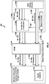
- FIG. 1 is a block diagram of a system 100 including an exemplary SSD having an NVM with on-chip PCA components. More specifically, the system 100 includes a host 102 and a SSD 104 (or other DSD) coupled to the host 102 .
- the host 102 provides commands to the SSD 104 for transferring data between the host 102 and the SSD 104 .
- the host 102 may provide a write command to the SSD 104 for writing data to the SSD 104 or read command to the SSD 104 for reading data from the SSD 104 .
- the host 102 may be any system or device having a need for data storage or retrieval and a compatible interface for communicating with the SSD 104 .
- the host 102 may a computing device, a personal computer, a portable computer, a workstation, a server, a personal digital assistant, a digital camera, or a digital phone as merely a few examples.
- the host 102 may be a system or device having a need for neural network processing, such as speech recognition systems and computer vision systems.
- the host 102 may be a component of an aerial drone, autonomous vehicle, etc.
- the SSD 104 includes a host interface 106 , an SSD or DSD controller 108 , a volatile memory 110 (such as DRAM or other working memory), an NVM interface 112 (which may be referred to as a flash interface), and an NVM die or dies 114 configured with on-chip PCA components and with a NAND array.
- the host interface 106 is coupled to the controller 108 and facilitates communication between the host 102 and the controller 108 .
- the controller 108 is coupled to the volatile memory 110 as well as to the NVM die(s) 114 via the NVM interface 112 .
- the host interface 106 may be any suitable communication interface, such as a Non-Volatile Memory express (NVMe) interface, a Universal Serial Bus (USB) interface, a Serial Peripheral (SP) interface, an Advanced Technology Attachment (ATA) or Serial Advanced Technology Attachment (SATA) interface, a Small Computer System Interface (SCSI), an IEEE 1394 (Firewire) interface, or the like.
- NVMe Non-Volatile Memory express
- USB Universal Serial Bus
- SP Serial Peripheral
- ATA Advanced Technology Attachment
- SATA Serial Advanced Technology Attachment
- SCSI Small Computer System Interface
- IEEE 1394 Firewire interface
- the host 102 includes the SSD 104 .
- the SSD 104 is remote from the host 102 or is contained in a remote computing system communicatively coupled with the host 102 .
- the host 102 may communicate with the SSD 104 through a wireless communication link.
- SSD 104 includes a single channel between controller 108 and NVM die(s) 114 via interface 112
- the subject matter described herein is not limited to having a single memory channel.
- two, four, eight or more NAND channels couple the controller and the NAND memory device, depending on controller capabilities.
- more than a single channel may be used between the controller and the memory die, even if a single channel is shown in the drawings.
- the controller 108 may be implemented in a single integrated circuit chip and may communicate with different layers of memory in the NVM die(s) 114 over one or more command channels.
- the controller 108 controls operation of the SSD 104 .
- the controller 108 receives commands from the host 102 through the host interface 106 and performs the commands to transfer data between the host 102 and the NVM die(s) 114 .
- the controller 108 may manage reading from and writing to volatile memory 110 for performing the various functions effected by the controller and to maintain and manage cached information stored in volatile memory 110 .
- the controller 108 may include any type of processing device, such as a microprocessor, a microcontroller, an embedded controller, a logic circuit, software, firmware, or the like, for controlling operation of the SSD 104 .
- some or all of the functions described herein as being performed by the controller 108 may instead be performed by another element of the SSD 104 .
- the SSD 104 may include a microprocessor, a microcontroller, an embedded controller, a logic circuit, software, firmware, application specific integrated circuit (ASIC), or any kind of processing device, for performing one or more of the functions described herein as being performed by the controller 108 .
- one or more of the functions described herein as being performed by the controller 108 are instead performed by the host 102 .
- some or all of the functions described herein as being performed by the controller 108 may instead be performed by another element such as a controller in a hybrid drive including both non-volatile memory elements and magnetic storage elements.
- the volatile memory 110 may be any suitable memory, computing device, or system capable of storing data.
- the volatile memory 110 may be ordinary RAM, DRAM, double data rate (DDR) RAM, static RAM (SRAM), synchronous dynamic RAM (SDRAM), a flash storage, an erasable programmable read-only-memory (EPROM), an electrically erasable programmable ROM (EEPROM), or the like.
- the controller 108 uses the volatile memory 110 , or a portion thereof, to store data during the transfer of data between the host 102 and the NVM die(s) 114 .
- the volatile memory 110 or a portion of the volatile memory 110 may be a cache memory.
- the NVM die(s) 114 receives data from the controller 108 via the NVM interface 112 and stores the data.
- the NVM die(s) 114 may be any suitable type of non-volatile memory, such as a NAND-type flash memory array die or the like.
- volatile memory 110 may be replaced by a non-volatile memory such as MRAM, PCM, ReRAM, etc. to serve as a working memory for the overall device.
- the controller 108 may include hardware, firmware, software, or any combinations thereof that provide a machine learning controller 116 for use with the NVM die(s) 114 (where the machine learning controller, in some examples, may include at least some off-chip control components such as components for controlling the PCA components on the NVM die(s) 114 ).
- FIG. 1 shows an exemplary SSD and an SSD is generally used as an illustrative example in the description throughout, the various disclosed embodiments are not necessarily limited to an SSD application/implementation.
- the disclosed NVM die and associated processing components can be implemented as part of a package that includes other processing circuitry and/or components.
- a processor may include, or otherwise be coupled with, embedded NVM and associated circuitry and/or components for machine learning that are described herein.
- the processor could, as one example, off-load certain machine learning tasks to the NVM and associated circuitry and/or components.
- the controller 108 may be a controller in another type of device and still include the machine learning controller 116 and perform some or all of the functions described herein.
- FIG. 2 is a block diagram illustrating selected components of an exemplary SSD 200 having a machine learning engine 216 (which may be a component of a data storage controller), a DRAM 210 (which also may be a component of a data storage controller), and an NVM device 214 (which may comprise one or more NVM dies).
- the machine learning engine 216 may include one or more processors such as ASICs or CPUs (not shown) or may be a portion of a processor (such as an ASIC or CPU).
- the NVM device 214 includes, in this example, NVM storage elements 218 (such as NAND arrays or ReRAM arrays) and on-chip PCA components 220 (which may be implemented in hardware or firmware on the die as under-the-array, next-to-the-array, or other extra-array processing components formed in or on or below the die).
- NVM storage elements 218 such as NAND arrays or ReRAM arrays
- on-chip PCA components 220 which may be implemented in hardware or firmware on the die as under-the-array, next-to-the-array, or other extra-array processing components formed in or on or below the die.
- machine learning (ML) data having D dimensions is stored within the NVM storage elements 218 .
- the data may be referred to as “input” data since the data is meant for eventual input into the machine learning engine 216 .
- the D-dimensional ML data 222 may be, for example, training data for training a DNN (not shown) associated with the machine learning engine 216 .
- the machine learning engine 216 is configured for image recognition and the data consists of a large set of images for training the image recognition system of the machine learning engine.
- the D-dimensional data 222 is transferred from the NVM storage elements 218 to the on-chip PCA components 220 , which perform PCA operations to generate PCA output data, such as by converting correlated data within the input D-dimensional data 222 into linearly uncorrelated values that represent the principal components of the data.
- the resulting principal components i.e. the PCA output data
- M is smaller than D and, typically, where M is much smaller than D, hence providing for on-chip dimensionality reduction.
- D is greater than 10,000, whereas M is less than 10. In one particular example, D is 83,781 and M is 4. Hence, a significant reduction in dimensionality is achieved within the PCA output data.
- one or more page buffers may be used for temporarily storing data obtained from the NVM storage elements 218 for use during the PCA operations, such as for storing intermediate computed values.
- the resulting M-dimensional ML data 224 is then transferred from the NVM device 214 into the DRAM 210 , where it is stored, and then transferred to, or accessed as needed by, the machine learning engine 216 .
- the machine learning engine 216 may output data to other components of the SSD 200 or to a host (not shown).
- the output data may include, e.g., values representative of a trained DNN, such as suitable synaptic weights, etc.
- the PCA components 220 of FIG. 2 may be configured to determine the principal components of the D-dimensional data to yield M-dimensional data using PCA.
- PCA thus may be used as a preprocessing technique to significantly reduce the complexity of the neural networks.
- PCA may achieve this goal by reducing the dimensionality of an input space after a wavelet analysis while preserving as much of the relevant information as possible.
- FIG. 3 illustrates an exemplary method that may be performed by the NVM device 214 of FIG. 3 or other suitably-equipped devices.
- the NVM device (consisting of one or more dies of an SSD) inputs an initial set of input images into an NVM array of the NVM device for use with image recognition training (or inputs other sets of input data for use with other forms of machine learning).
- the data may be input, for example, from the data storage controller of the SSD in response to commands (e.g. write commands) issued by a host device coupled to the SSD.
- the NVM device reads one or more of the images or other stored machine learning data from the NVM array for on-chip PCA processing, where the images or other machine learning data have D-dimensionality.
- the NVM device applies on-chip PCA to the images or other data to convert correlated portions of the images or other data into linearly uncorrelated values that represent the principal components of the images or other data, where the principal components have M-dimensionality, so as to achieve the aforementioned on-chip dimensionality reduction.
- the NVM device outputs the M-dimensional principal components to an off-chip device, such as a data storage controller of the SSD or a host device, for performing machine learning to, for example, train an image recognition system of the host to recognize images.
- the aim of the on-chip PCA is to map vectors x in a d-dimensional input space (x 1 , . . . , x d ) onto vectors z in a lower M-dimensional space (z 1 , . . . , z M ) in such a way that any loss of important information and data variation needed for classification (e.g. image recognition) is minimized while keeping M ⁇ d.
- the PCA components 220 of FIG. 2 may be configured to represent x as a linear combination of a set of d orthonormal vectors u i in the form,
- the PCA components may be further configured to retain only a subset M ⁇ d of the basis vectors u i using z i to form
- x′ is the approximation to x.
- the remaining values z i for i ⁇ M+1 may be replaced by constants b i .
- the minimum of the sum of the squares of the errors may be computed using
- FIG. 4 is a block diagram illustrating selected components of an exemplary SSD 400 having an NVM device that includes on-chip components configured to perform PCA to generate eigenvalues and eigenvectors.
- SSD 400 again includes a machine learning engine 416 , a DRAM 410 , and an NVM device 414 (which may comprise one or more dies).
- the NVM device 414 again includes NVM storage elements 418 and PCA components 420 .
- ML data with dimension D is again stored within the NVM storage elements 418 .
- the D-dimensional data 422 is transferred from the NVM storage elements 418 to the PCA components 420 , which perform eigenvalue and eigenvector-based PCA operations to convert correlated data within the input D-dimensional data 422 into linearly uncorrelated values that represent the principal components of the data, which may be represented as M-dimensional data 424 .
- the PCA components 420 perform eigenvalue and eigenvector-based PCA operations to convert correlated data within the input D-dimensional data 422 into linearly uncorrelated values that represent the principal components of the data, which may be represented as M-dimensional data 424 .
- one or more page buffers may be used for temporarily storing data during the PCA operations performed by PCA components 220 , such as intermediate computed values.
- the machine learning engine 416 is configured to perform machine learning based on an initial set of eigenvalues and corresponding eigenvectors and then using subsequent sets of eigenvalues without corresponding eigenvectors.
- This may be regarded as a form of feature extraction. That is, in this example, the machine learning engine 416 includes a feature extraction system 417 (or is a feature extraction system).
- the PCA components 420 are configured to generate an initial set of eigenvectors and eigenvalues based on an initial set of D-dimensional ML data and to then generate additional eigenvalues (but not additional eigenvectors) for additional sets of data.
- the initial set of D-dimensional ML data may include an initial set of training images from which eigenvectors and eigenvalues are generated.
- the additional sets of data may include additional training images from which eigenvalues are generated for use with the initial set of eigenvectors.
- an initial set of M-dimensional ML data 424 (consisting of eigenvalues and initial eigenvectors) is transferred from the NVM device 414 into the DRAM 410 , where it is stored and then accessed as needed by the machine learning engine 416 and its feature extraction system 417 to perform initial training. Then, additional sets of M-dimensional ML data 424 (consisting of eigenvalues without eigenvectors) are transferred from the NVM device 414 into the DRAM 410 , where it is stored and then accessed as needed by the machine learning engine 416 and its feature extraction system 417 to perform further training.
- the machine learning engine 416 and its feature extraction system 417 may output data to other components of the SSD 400 or to a host (not shown).
- the output data again may include, for example, values representative of a trained DNN, such as synaptic weights or the like.
- FIG. 5 is a block diagram illustrating selected components of an exemplary SSD 500 having an NVM device that outputs eigenvalues without outputting any corresponding eigenvectors.
- the SSD 500 again includes a machine learning engine 516 , a DRAM 510 , and an NVM device 514 (which may comprise one or more dies).
- the NVM device 514 again includes NVM storage elements 518 and on-chip PCA components 520 .
- a set of ML data with dimension D is again stored within the NVM storage elements 518 .
- the D-dimensional data 522 is transferred from the NVM storage elements 518 to the PCA components 520 , which perform PCA operations to convert the input D-dimensional data 522 into M-dimensional data 524 .
- the machine learning engine 516 is configured to perform machine learning based on eigenvalues without the need for eigenvectors. This also may be regarded as a form of feature extraction, and the machine learning engine 516 is shown to include a feature extraction system 517 .
- the PCA components 520 are configured to generate and output eigenvalues based on D-dimensional ML data. Any eigenvectors generated as part of the PCA procedure are not output from the NVM device 514 to the machine learning engine 516 . In the example of FIG.
- the M-dimensional ML data 524 (consisting of the eigenvalues but not eigenvectors) is transferred from the NVM device 514 into the DRAM 510 , where it is stored and then accessed as needed by the machine learning engine 516 and its feature extraction system 517 .
- the machine learning engine 516 and its feature extraction system 517 may output data such as such as synaptic weights or the like.
- FIG. 6 is a block diagram illustrating selected components of an exemplary SSD 600 having an NVM device that includes components configured for PCA bypass.
- the SSD 600 again includes a machine learning engine 616 , a DRAM 610 , and an NVM device 614 (which may comprise one or more dies).
- the machine learning engine 616 includes a bypass controller 615 for selectively controlling the NVM device 614 to bypass at least some of its on-chip PCA components.
- the NVM device or die 614 again includes NVM storage elements 618 and PCA components 620 .
- a set of ML data with dimension D is again stored within the NVM storage elements 618 .
- the D-dimensional data 622 is transferred from the NVM storage elements 618 to the PCA components 620 , which perform various PCA operations to convert the data to M-dimensional data 624 representative of the principal components of the data.
- the M-dimensional ML data 624 is transferred from the NVM device 614 into the DRAM 610 , where it is stored and then accessed as needed by the machine learning engine 616 .
- the PCA components 620 of the NVM device 618 are instead bypassed (as may be indicated by a suitable bypass command/control signal 621 sent from bypass controller 615 to the NVM device 614 )
- the D-dimensional ML data 622 is transferred to the DRAM 610 and then to the machine learning engine 616 .
- command signal 621 may be used to control the amount of PCA that is performed by the on-chip PCA components 620 to, for example, control the amount of dimensional reduction that is achieved by, for example, specifying the value of M to be achieved.
- FIG. 7 is a block diagram illustrating selected components of an exemplary SSD 700 having an NVM device that includes storage array components configured for matrix multiplication.
- the SSD 700 again includes machine learning engine 716 , a DRAM 710 , and an NVM device 714 (which may comprise one or more dies).
- the NVM device 714 again includes NVM storage elements 718 and PCA components 720 .
- a portion of the NVM storage elements 718 is configured as a matrix multiplication core 721 for directly performing matrix multiplication operations (such as covariance matrix computations).
- a controller 723 within the PCA components 720 controls the operation of the matrix multiplication core 721 .
- ML data with dimension D is processed by the PCA components 720 and the matrix multiplication core 721 (under the control of the matrix multiplication controller 723 ) to convert the D-dimensional data to M-dimensional data 724 .
- the matrix multiplication core of storage array 721 may have suitable weight values for PCA already stored therein or those values may be obtained from other NVM elements 718 . Since at least some of the PCA operations are performed by the matrix multiplication core of the NVM storage array 721 , it may possible (depending on the particular configuration of the PCA components 720 ) to use fewer or smaller page buffers during the PCA operations.
- the resulting M-dimensional ML data 724 is transferred from the NVM device 714 into the DRAM 710 , where it is stored and then accessed as needed by the machine learning engine 716 .
- FIG. 8 illustrates an exemplary configuration for the NVM storage array 721 of FIG. 7 for performing matrix multiplications.
- FIG. 8 also illustrates exemplary N ⁇ M matrix multiplication operations 726 that may be performed by the NVM storage array 721 (for use as part of a PCA procedure to determine principal components or for other purposes).
- Individual elements (digital values) of the input matrix are applied to digital-to-analog converters (DAC) 730 to generate analog voltage values (V 1 . . . N ), which are then applied to individual storage elements 732 of the array, which are configured to represent individual weights (W nm ) of the weight matrix (W NM ).
- each separate voltage value (V n ) correspond to the input matrix I is applied to a row of the storage elements 732 .
- FIG. 8 illustrates an exemplary configuration for the NVM storage array 721 of FIG. 7 for performing matrix multiplications.
- FIG. 8 also illustrates exemplary N ⁇ M matrix multiplication operations 726 that may be performed by the NVM storage array 721 (for use as part of a PCA procedure to determine principal components or for other purposes).
- Individual elements (digital values) of the input matrix are applied to digital-to-analog converters (DAC) 730 to generate analog voltage values (V 1 . . . N ), which are then applied to individual storage elements 732 of the array, which are configured to represent individual weights (W nm ) of the weight matrix (W NM ).
- each separate voltage value (V n ) corresponds to the input matrix I is applied to a row of the storage elements 732 .
- FIG. 9 is a block diagram illustrating selected components of an exemplary SSD 900 where the NVM device includes ECC components for performing error detection and correction on D-dimensional data before PCA processing of the data.
- the SSD 900 includes a machine learning engine 916 , a DRAM 910 , and an NVM device 914 (which may comprise one or more dies).
- the NVM device 914 again includes NVM storage elements 918 and PCA components 920 .
- the NVM device 914 also includes an ECC component 919 .
- ML data with dimension D is stored within the NVM storage elements 918 .
- the ML D-dimensional data 922 is transferred from the NVM storage elements 918 to the ECC component 919 , which applies error correction codes to correct errors in the ML D-dimensional data.
- the error-corrected ML D-dimensional data 922 is transferred to the PCA components 920 , which perform PCA operations to determine the principal components of the data, which may be represented as M-dimensional data 924 .
- the M-dimensional ML data 924 is transferred from the NVM device 914 into the DRAM 910 , where it is stored and then accessed as needed by the machine learning engine 916 to perform initial training.
- the machine learning engine 916 may output data to other components of the SSD 900 or to a host (not shown).
- the output data again may include, for example, values representative of a trained DNN, such as synaptic weights or the like.
- FIG. 10 is a block diagram illustrating selected components of an exemplary SSD 1000 where the NVM device includes ECC components for performing error detection and correction on the M-dimensional data after PCA processing.
- the SSD 1000 again includes a machine learning engine 1016 , a DRAM 1010 , and an NVM device 1014 (which may comprise one or more dies).
- the NVM device or die 1014 includes NVM storage elements 1018 , PCA components 1020 , and an ECC component 1021 .
- ML data with dimension D is stored within the NVM storage elements 1018 .
- Uncorrected ML D-dimensional data 1022 is transferred from the NVM storage elements 1018 to the PCA components 1020 , which perform PCA operations to determine the principal components of the data, which may be represented as M-dimensional data 1024 .
- the ML M-dimensional data 1024 is then processed by the ECC component 1021 , which applies error correction codes to correct errors in the ML M-dimensional data.
- the error-corrected ML M-dimensional data 1024 is transferred from the NVM device 1014 to the DRAM 1010 , where it is stored and then accessed as needed by the machine learning engine 1016 to perform initial training.
- FIG. 11 is a block diagram of an exemplary NVM die 1100 that includes NVM storage array components 1102 and under-the-array or next-to-the-array (or other extra-array) processing components 1104 for performing PCA and other functions. Not all circuit or memory components that might be used in a practical NVM die are illustrated in the figure, such as input and output components, voltage regulation components, clocks and timing components, etc. Rather selected components and circuits are shown, summarized as block or schematic diagrams.
- the exemplary NVM array components 1102 include: NVM storage 1106 for storing machine learning training data such as input image data; and NVM storage 1108 configured for storing other data such as DNN synaptic weights, bias values, etc., or other types of user data or system data.
- the NVM extra-array processing components 1104 include various PCA components 1110 configured to perform or control PCA operations.
- the exemplary PCA components 1110 include: one or more dimensionality reduction controllers 1112 configured to control PCA operations to reduce a dimensionality of the input image data from D to M where D>>M (and where M can be selected or otherwise controlled); one or more eigenvalue generation components 1114 configured to determine or generate eigenvalues from the input data; one or more eigenvector generation components 1116 configured to determine or generate eigenvalues from the input data; and one or more page buffers 1118 configured to store intermediate data.
- some of these components may be replaced by or supplemented by a matrix multiplication core (shown in FIG. 8 and discussed above).
- each of the individual PCA components 1112 , 1114 , 1116 , and 1118 ) are shown since, in some examples, a plurality of such components may operate in parallel.
- N PCA components 1110 may be provided to concurrently process N different input training images to expedite PCA processing.
- only a single instance of each component may be provided.
- other PCA components are additionally or alternatively provided, which serve to perform additional or alternative PCA procedures.
- the NVM extra-array processing components 1104 of FIG. 11 also include various other components including: a machine learning data input controller 1126 configured to input and store machine learning training data in the NVM storage 1106 ; a machine learning data output controller 1128 configured to output principal component data (such as eigenvalues and eigenvectors) and other data as may be appropriate (such as synaptic weights) depending on the particular PCA procedure being implemented and the particular the DNN for use with the machine learning data; and an on-chip ECC component 1130 configured to control any on-chip ECC applied to data as it is read from the NVM array components 1102 (and/or after it has been processed by the PCA components).
- a PCA bypass controller 1132 is provided, which operates as discussed above to selectively bypass PCA so D-dimensional data may be output.
- a wear leveling controller 1134 performs wear leveling of data stored in the NVM device 1100 .
- a “Read with PCA” command may be enabled for reading out data from the NVM device 1100 while performing PCA.
- the data may be read out of the NVM core storage 1106 using page reads and stored in the page buffers 1118 for PCA processing. This is summarized in the next figure.
- FIG. 12 summarizes an example of processing by an NVM device in response to a received “Read with PCA” command.
- the NVM device receives the “Read with PCA” command from a data storage controller (e.g., controller 108 in FIG. 1 ).
- the NVM device reads input data from NVM core array in parallel (e.g., a page read) or in series or in series-parallel combination and stores the data in a page buffer or other storage space. (Here, again, the data is referred to as input data since it is meant for input into a machine learning system for training purposes or other purposes.)
- the NVM device performs PCA processing on the retrieved input data to generate lower dimensional data, i.e.
- the NVM device outputs (e.g. fetches out) the lower dimensional data through an input/output module from the NVM device to a DRAM or other storage device for use with machine learning, where the machine learning may be performed by the data storage controller or a host device.
- FIG. 13 broadly illustrates a process 1300 in accordance with aspects of the disclosure.
- the process 1300 may take place within any suitable memory die with an NVM array where the die is capable of performing the operations, such as a memory die provided with under-the-array circuitry coupled to a NAND array.
- the memory die stores data (such as training data for machine learning) within its NVM array.
- the memory die determines one or more principal components of the data using a PCA component formed within the die. For example, under-the-array circuitry formed in the memory die may apply the data to under-the-array PCA components to generate PCA output data where the PCA output data comprises the principal components.
- PCA output data may include eigenvalues and eigenvectors.
- the memory die outputs the one or more principal components of the data.
- the data may be output, for example, to a data storage controller of an SSD (of which the memory die is a component or is operationally coupled to).
- FIG. 14 broadly illustrates a process 1400 in accordance with other aspects of the disclosure, where error correction codes are applied after PCA.
- the process 1400 may take place within any suitable memory die capable of performing the operations.
- the memory die reads previously-stored input data from NVM elements of the die, where the data is representative of machine learning training data such as image data.
- the memory die applies the input data to an on-chip PCA component formed within the memory die to identify principal components of the input data by, for example, (1) determining eigenvalues and eigenvectors for a first set of input data and determining eigenvalues without eigenvectors for a plurality of subsequent sets of input data; or (2) determining eigenvalues and eigenvectors for all sets of input data.
- the memory die applies error correction codes using an on-chip ECC component to the data output from the PCA component.
- the memory die outputs the error-corrected principal component data to an off-chip device by, for example, (1) outputting eigenvalues and eigenvectors for the first set of input data and outputting eigenvalues without eigenvectors for the plurality of subsequent sets of input data; or (2) outputting eigenvalues only for all sets of data, and outputting other machine learning data that may be appropriate such as synaptic weights.
- FIG. 15 broadly illustrates a process 1500 in accordance with still other aspects of the disclosure, where error correction codes are applied before PCA.
- the process 1500 may take place within any suitable memory die capable of performing the operations.
- the memory die reads previously-stored input data from NVM elements of the NVM die, where the data is again representative of machine learning training data such as image data.
- the memory die applies error correction codes using an on-chip ECC to the data read from the NVM memory elements.
- the memory die applies the error-corrected data to an on-chip PCA component formed within the memory die to identify principal components of the input data by, for example, (1) determining eigenvalues and eigenvectors for a first set of error-corrected input data and determining eigenvalues without eigenvectors for a plurality of subsequent sets of error-corrected input data; or (2) determining eigenvalues and eigenvectors for all sets of error-corrected input data.
- the memory die outputs the principal components to an off-chip device by, for example, (1) outputting eigenvalues and eigenvectors for the first set of input data and outputting eigenvalues without eigenvectors for the plurality of subsequent sets of input data; or (2) outputting eigenvalues only for all sets of data, and outputting other machine learning data that may be appropriate such as synaptic weights.
- FIG. 16 broadly illustrates a memory die 1600 configured according to one or more aspects of the disclosure.
- the memory die 1600 includes an NVM array 1602 , such as a NAND or ReRAM array.
- the memory die also includes a PCA component 1604 configured in the memory die to process input data obtained from the NVM array 1602 to generate PCA output data.
- the memory die also includes an output device 1606 configured to output the PCA output data from the memory die.
- the PCA output data may be output, e.g., to a data storage controller of an SSD (of which the memory die is a component or is operationally coupled to). Examples are described above. Additional examples are described below.
- an apparatus formed on a memory die may be provided where the memory die has an NVM array and where the apparatus includes: means, such as PCA component 1604 of FIG. 16 , for performing PCA on data obtained from the NVM array to determine principal components of the data; and means, such as output device 1606 of FIG. 16 , for outputting the principal components of the data from the memory die.
- FIG. 17 illustrates an embodiment of an apparatus 1700 configured according to one or more aspects of the disclosure.
- the apparatus 1700 or components thereof, could embody or be implemented within a NAND die or some other type of NVM device or memory die that supports data storage.
- the apparatus 1700 or components thereof, could be a component of a processor, a controller, a computing device, a personal computer, a portable device, or workstation, a server, a personal digital assistant, a digital camera, a digital phone, an entertainment device, a medical device, a self-driving vehicle control device, aerial drone, smart glasses, smart watch or other wearable device, or any other electronic device that stores, processes or uses data.
- the apparatus 1700 includes a communication interface 1702 , a physical memory array (e.g., NAND blocks or NAND pages) 1704 , and extra-array processing circuits 1710 (e.g. under-the-array or next-to-the-array circuits). These components can be coupled to and/or placed in electrical communication with one another via suitable components, represented generally by the connection lines in FIG. 17 . Although not shown, other circuits such as timing sources, peripherals, voltage regulators, and power management circuits may be provided, which are well known in the art, and therefore, will not be described any further.
- the communication interface 1702 provides a means for communicating with other apparatuses over a transmission medium.
- the communication interface 1702 includes circuitry and/or programming (e.g., a program) adapted to facilitate the communication of information bi-directionally with respect to one or more devices in a system.
- the communication interface 1702 may be configured for wire-based communication.
- the communication interface 1702 could be a bus interface, a send/receive interface, or some other type of signal interface including circuitry for outputting and/or obtaining signals (e.g., outputting signal from and/or receiving signals into an SSD).
- the communication interface 1702 serves as one example of a means for receiving and/or a means for transmitting.
- the physical memory array 1704 may represent one or more NAND blocks or pages.
- the physical memory array 1704 may be used for storing data such images that are manipulated by the circuits 1710 or some other component of the apparatus 1700 .
- the physical memory array 1704 may be coupled to the circuits 1710 such that the circuits 1710 can read or sense information from, and write or program information to, the physical memory array 1704 . That is, the physical memory array 1704 can be coupled to the circuits 1710 so that the physical memory array 1704 is accessible by the circuits 1710 .
- Data may be temporarily stored in one or more page buffers 1711 .
- the circuits 1710 are arranged or configured to obtain, process and/or send data, control data access and storage, issue or respond to commands, and control other desired operations.
- the circuits 1710 may be implemented as one or more processors, one or more controllers, and/or other structures configured to perform functions.
- the circuits 1710 may be adapted to perform any or all of the extra-array features, processes, functions, operations and/or routines described herein.
- the circuits 1710 may be configured to perform any of the steps, functions, and/or processes described with reference to the other figures.
- the term “adapted” in relation to the processing circuits 1710 may refer to the circuits being one or more of configured, employed, implemented, and/or programmed to perform a particular process, function, operation and/or routine according to various features described herein.
- the circuits may include a specialized processor, such as an ASIC that serves as a means for (e.g., structure for) carrying out any one of the operations described with reference to the other figures.
- the circuits serve as an example of a means for processing.
- the circuits may provide and/or incorporate, at least in part, functionality described above for the on-chip PCA components in various embodiments shown, including for example element 220 of FIG. 2 .
- the processing circuit 1710 may include one or more of: circuit/modules 1720 configured for storing images or other machine learning data in NVM pages; circuits/modules 1722 configured for reading images or other machine learning data from NVM pages; circuits/modules 1724 configured for applying ECC to the images or other machine learning data (as they are read out of the NVM blocks); circuits/modules 1726 performing PCA; circuits/modules 1728 configured for bypassing the PCA operations; circuits/modules 1730 configured for determining eigenvalues and eigenvectors for a first set of input data and determining eigenvalues without eigenvectors for subsequent sets of input data; circuits/modules 1732 configured for determining eigenvalues without generating corresponding eigenvectors; and circuits/modules 1734 configured for applying ECC to PCA output data (before the PCA output data is output from the apparatus 1700 .
- circuits/modules 1720 configured for storing images or other
- means may be provided for performing the functions illustrated in FIG. 17 and/or other functions illustrated or described herein.
- the means may include one or more of: means, such as circuit/modules 1720 , for storing images or other machine learning data in the NVM; means, such as circuits/modules 1722 , for reading images or other machine learning data from the NVM; means, such as circuits/modules 1724 , for applying ECC to the images or other machine learning data; means, such as circuits/modules 1726 , for performing PCA; means, such as circuits/modules 1728 , for bypassing PCA; means, such as circuits/modules 1730 , for determining eigenvalues and eigenvectors for a first set of input data and determining eigenvalues without eigenvectors for subsequent sets of input data; means, such as circuits/modules 1732 , for determining eigenvalues without generating corresponding eigenvectors;
- processing circuits described herein may be generally adapted for processing, including the execution of programming code stored on a storage medium.
- code or “programming” shall be construed broadly to include without limitation instructions, instruction sets, data, code, code segments, program code, programs, programming, subprograms, software modules, applications, software applications, software packages, routines, subroutines, objects, executables, threads of execution, procedures, functions, etc., whether referred to as software, firmware, middleware, microcode, hardware description language, or otherwise.
- processing circuits described herein may be arranged to obtain, process and/or send data, control data access and storage, issue commands, and control other desired operations.
- the processing circuits may include circuitry configured to implement desired programming provided by appropriate media in at least one example.
- the processing circuits may be implemented as one or more processors, one or more controllers, and/or other structure configured to execute executable programming.
- Examples of processing circuits may include a general purpose processor, a digital signal processor (DSP), an ASIC, a field programmable gate array (FPGA) or other programmable logic component, discrete gate or transistor logic, discrete hardware components, or any combination thereof designed to perform the functions described herein.
- a general purpose processor may include a microprocessor, as well as any conventional processor, controller, microcontroller, or state machine. At least some of the processing circuits may also be implemented as a combination of computing components, such as a combination of a controller and a microprocessor, a number of microprocessors, one or more microprocessors in conjunction with an ASIC and a microprocessor, or any other number of varying configurations.
- the various examples of processing circuits noted herein are for illustration and other suitable configurations within the scope of the disclosure are also contemplated.
- NVM non-volatile memory
- semiconductor memory devices include working memory devices, such as DRAM or SRAM devices, NVM devices, ReRAM, EEPROM, flash memory (which can also be considered a subset of EEPROM), ferroelectric random access memory (FRAM), and MRAM, and other semiconductor elements capable of storing information.
- working memory devices such as DRAM or SRAM devices
- NVM devices Non-Volatile Memory
- ReRAM ReRAM
- EEPROM electrically erasable programmable read-only memory
- flash memory which can also be considered a subset of EEPROM
- FRAM ferroelectric random access memory
- MRAM ferroelectric random access memory
- flash memory devices may be configured in a NAND or a NOR configuration.
- some features described herein are specific to NAND-based devices, such as the NAND-based on-chip copy with update.
- the memory devices can be formed from passive and/or active elements, in any combinations.
- passive semiconductor memory elements include ReRAM device elements, which in some embodiments include a resistivity switching storage element, such as an anti-fuse, phase change material, etc., and optionally a steering element, such as a diode, etc.
- active semiconductor memory elements include EEPROM and flash memory device elements, which in some embodiments include elements containing a charge storage region, such as a floating gate, conductive nanoparticles, or a charge storage dielectric material.
- Associated circuitry is typically required for operation of the memory elements and for communication with the memory elements.
- memory devices may have circuitry used for controlling and driving memory elements to accomplish functions such as programming and reading.
- This associated circuitry may be on the same substrate as the memory elements and/or on a separate substrate.
- a controller for memory read-write operations may be located on a separate controller chip and/or on the same substrate as the memory elements.
- the subject matter described herein may be implemented in hardware, software, firmware, or any combination thereof.
- the terms “function,” “module,” and the like as used herein may refer to hardware, which may also include software and/or firmware components, for implementing the feature being described.
- the subject matter described herein may be implemented using a computer readable medium having stored thereon computer executable instructions that when executed by a computer (e.g., a processor) control the computer to perform the functionality described herein.
- Examples of computer readable media suitable for implementing the subject matter described herein include non-transitory computer-readable media, such as disk memory devices, chip memory devices, programmable logic devices, and application specific integrated circuits.
- a computer readable medium that implements the subject matter described herein may be located on a single device or computing platform or may be distributed across multiple devices or computing platforms.
- any reference to an element herein using a designation such as “first,” “second,” and so forth does not generally limit the quantity or order of those elements. Rather, these designations may be used herein as a convenient method of distinguishing between two or more elements or instances of an element. Thus, a reference to first and second elements does not mean that only two elements may be used there or that the first element must precede the second element in some manner. Also, unless stated otherwise a set of elements may include one or more elements.
- terminology of the form “at least one of A, B, or C” or “A, B, C, or any combination thereof” used in the description or the claims means “A or B or C or any combination of these elements.”
- this terminology may include A, or B, or C, or A and B, or A and C, or A and B and C, or 2 A, or 2 B, or 2 C, or 2 A and B, and so on.
- “at least one of: A, B, or C” is intended to cover A, B, C, A-B, A-C, B-C, and A-B-C, as well as multiples of the same members (e.g., any lists that include AA, BB, or CC).
- “at least one of: A, B, and C” is intended to cover A, B, C, A-B, A-C, B-C, and A-B-C, as well as multiples of the same members.
- a phrase referring to a list of items linked with “and/or” refers to any combination of the items.
- “A and/or B” is intended to cover A alone, B alone, or A and B together.
- “A, B and/or C” is intended to cover A alone, B alone, C alone, A and B together, A and C together, B and C together, or A, B, and C together.
- determining encompasses a wide variety of actions. For example, “determining” may include calculating, computing, processing, deriving, investigating, looking up (e.g., looking up in a table, a database or another data structure), ascertaining, and the like. Also, “determining” may include receiving (e.g., receiving information), accessing (e.g., accessing data in a memory), and the like. Also, “determining” may include resolving, selecting, choosing, establishing, and the like.
Abstract
Description
The PCA components may be further configured to retain only a subset M<d of the basis vectors ui using zi to form
where x′ is the approximation to x. The remaining values zi for i≥M+1 may be replaced by constants bi. The minimum of the sum of the squares of the errors may be computed using
taken over the whole data set (n=1, N), thus yielding the vector z with components zi (i=1, M), which approximates x in the M-dimensional input space.
Claims (24)
Priority Applications (3)
| Application Number | Priority Date | Filing Date | Title |
|---|---|---|---|
| US16/706,618 US11216184B2 (en) | 2019-12-06 | 2019-12-06 | Non-volatile memory with on-chip principal component analysis for generating low dimensional outputs for machine learning |
| PCT/US2020/038773 WO2021112920A1 (en) | 2019-12-06 | 2020-06-19 | Non-volatile memory with on-chip principal component analysis for generating low dimensional outputs for machine learning |
| US17/545,926 US11662904B2 (en) | 2019-12-06 | 2021-12-08 | Non-volatile memory with on-chip principal component analysis for generating low dimensional outputs for machine learning |
Applications Claiming Priority (1)
| Application Number | Priority Date | Filing Date | Title |
|---|---|---|---|
| US16/706,618 US11216184B2 (en) | 2019-12-06 | 2019-12-06 | Non-volatile memory with on-chip principal component analysis for generating low dimensional outputs for machine learning |
Related Child Applications (1)
| Application Number | Title | Priority Date | Filing Date |
|---|---|---|---|
| US17/545,926 Continuation US11662904B2 (en) | 2019-12-06 | 2021-12-08 | Non-volatile memory with on-chip principal component analysis for generating low dimensional outputs for machine learning |
Publications (2)
| Publication Number | Publication Date |
|---|---|
| US20210173560A1 US20210173560A1 (en) | 2021-06-10 |
| US11216184B2 true US11216184B2 (en) | 2022-01-04 |
Family
ID=76209112
Family Applications (2)
| Application Number | Title | Priority Date | Filing Date |
|---|---|---|---|
| US16/706,618 Active 2039-12-30 US11216184B2 (en) | 2019-12-06 | 2019-12-06 | Non-volatile memory with on-chip principal component analysis for generating low dimensional outputs for machine learning |
| US17/545,926 Active US11662904B2 (en) | 2019-12-06 | 2021-12-08 | Non-volatile memory with on-chip principal component analysis for generating low dimensional outputs for machine learning |
Family Applications After (1)
| Application Number | Title | Priority Date | Filing Date |
|---|---|---|---|
| US17/545,926 Active US11662904B2 (en) | 2019-12-06 | 2021-12-08 | Non-volatile memory with on-chip principal component analysis for generating low dimensional outputs for machine learning |
Country Status (2)
| Country | Link |
|---|---|
| US (2) | US11216184B2 (en) |
| WO (1) | WO2021112920A1 (en) |
Cited By (3)
| Publication number | Priority date | Publication date | Assignee | Title |
|---|---|---|---|---|
| US20220100375A1 (en) * | 2019-12-06 | 2022-03-31 | Western Digital Technologies, Inc. | Non-volatile memory with on-chip principal component analysis for generating low dimensional outputs for machine learning |
| US20220107991A1 (en) * | 2020-10-01 | 2022-04-07 | International Business Machines Corporation | Fast pca of evolving data using analog crossbar array |
| US11366876B2 (en) * | 2020-06-24 | 2022-06-21 | International Business Machines Corporation | Eigenvalue decomposition with stochastic optimization |
Families Citing this family (4)
| Publication number | Priority date | Publication date | Assignee | Title |
|---|---|---|---|---|
| US11372585B2 (en) * | 2020-05-05 | 2022-06-28 | Micron Technology, Inc. | Asynchronous process topology in a memory device |
| US20210389909A1 (en) * | 2020-06-16 | 2021-12-16 | Samsung Electronics Co., Ltd. | Edge solid state drive (ssd) device and edge data system |
| US11893244B2 (en) | 2021-10-12 | 2024-02-06 | Western Digital Technologies, Inc. | Hybrid memory management of non-volatile memory (NVM) devices for use with recurrent neural networks |
| US11755208B2 (en) | 2021-10-12 | 2023-09-12 | Western Digital Technologies, Inc. | Hybrid memory management of non-volatile memory (NVM) devices for use with recurrent neural networks |
Citations (15)
| Publication number | Priority date | Publication date | Assignee | Title |
|---|---|---|---|---|
| US7457749B2 (en) | 2002-06-25 | 2008-11-25 | Microsoft Corporation | Noise-robust feature extraction using multi-layer principal component analysis |
| US20080319712A1 (en) * | 2007-06-22 | 2008-12-25 | Neptec Optical Solutions, Inc. | Discrete principal component analysis (dpca) |
| US20160029027A1 (en) | 2014-07-23 | 2016-01-28 | Samsung Electronics Co., Ltd. | Device and method for processing image |
| US20160345009A1 (en) | 2015-05-19 | 2016-11-24 | ScaleFlux | Accelerating image analysis and machine learning through in-flash image preparation and pre-processing |
| US20170045356A1 (en) * | 2015-08-14 | 2017-02-16 | Kla-Tencor Corporation | System, method and computer program product for calibration of metrology tools |
| US20180075344A1 (en) | 2016-09-09 | 2018-03-15 | SK Hynix Inc. | Neural network hardware accelerator architectures and operating method thereof |
| US20180150052A1 (en) * | 2016-11-30 | 2018-05-31 | Applied Materials, Inc. | Spectrographic monitoring using a neural network |
| US20180267810A1 (en) * | 2017-03-17 | 2018-09-20 | Sandisk Technologies Llc | On-die signal calibration |
| CN108629410A (en) | 2018-04-28 | 2018-10-09 | 中国科学院计算技术研究所 | Based on principal component analysis dimensionality reduction and/or rise the Processing with Neural Network method tieed up |
| CN108629409A (en) | 2018-04-28 | 2018-10-09 | 中国科学院计算技术研究所 | A kind of Processing with Neural Network system reducing IO expenses based on principal component analysis |
| US20180315159A1 (en) * | 2017-04-28 | 2018-11-01 | Intel Corporation | Compute optimizations for low precision machine learning operations |
| US20190004734A1 (en) * | 2017-06-30 | 2019-01-03 | Western Digital Technologies, Inc. | Operating parameter offsets in solid state memory devices |
| US20190198114A1 (en) * | 2017-12-21 | 2019-06-27 | Western Digital Technologies, Inc. | Programming to a correctable amount of errors |
| US20190347522A1 (en) * | 2018-05-11 | 2019-11-14 | Microsoft Technology Licensing, Llc | Training Set Sufficiency For Image Analysis |
| WO2020078470A1 (en) | 2018-10-18 | 2020-04-23 | 上海寒武纪信息科技有限公司 | Network-on-chip data processing method and device |
Family Cites Families (1)
| Publication number | Priority date | Publication date | Assignee | Title |
|---|---|---|---|---|
| US11216184B2 (en) * | 2019-12-06 | 2022-01-04 | Western Digital Technologies, Inc. | Non-volatile memory with on-chip principal component analysis for generating low dimensional outputs for machine learning |
-
2019
- 2019-12-06 US US16/706,618 patent/US11216184B2/en active Active
-
2020
- 2020-06-19 WO PCT/US2020/038773 patent/WO2021112920A1/en active Application Filing
-
2021
- 2021-12-08 US US17/545,926 patent/US11662904B2/en active Active
Patent Citations (15)
| Publication number | Priority date | Publication date | Assignee | Title |
|---|---|---|---|---|
| US7457749B2 (en) | 2002-06-25 | 2008-11-25 | Microsoft Corporation | Noise-robust feature extraction using multi-layer principal component analysis |
| US20080319712A1 (en) * | 2007-06-22 | 2008-12-25 | Neptec Optical Solutions, Inc. | Discrete principal component analysis (dpca) |
| US20160029027A1 (en) | 2014-07-23 | 2016-01-28 | Samsung Electronics Co., Ltd. | Device and method for processing image |
| US20160345009A1 (en) | 2015-05-19 | 2016-11-24 | ScaleFlux | Accelerating image analysis and machine learning through in-flash image preparation and pre-processing |
| US20170045356A1 (en) * | 2015-08-14 | 2017-02-16 | Kla-Tencor Corporation | System, method and computer program product for calibration of metrology tools |
| US20180075344A1 (en) | 2016-09-09 | 2018-03-15 | SK Hynix Inc. | Neural network hardware accelerator architectures and operating method thereof |
| US20180150052A1 (en) * | 2016-11-30 | 2018-05-31 | Applied Materials, Inc. | Spectrographic monitoring using a neural network |
| US20180267810A1 (en) * | 2017-03-17 | 2018-09-20 | Sandisk Technologies Llc | On-die signal calibration |
| US20180315159A1 (en) * | 2017-04-28 | 2018-11-01 | Intel Corporation | Compute optimizations for low precision machine learning operations |
| US20190004734A1 (en) * | 2017-06-30 | 2019-01-03 | Western Digital Technologies, Inc. | Operating parameter offsets in solid state memory devices |
| US20190198114A1 (en) * | 2017-12-21 | 2019-06-27 | Western Digital Technologies, Inc. | Programming to a correctable amount of errors |
| CN108629410A (en) | 2018-04-28 | 2018-10-09 | 中国科学院计算技术研究所 | Based on principal component analysis dimensionality reduction and/or rise the Processing with Neural Network method tieed up |
| CN108629409A (en) | 2018-04-28 | 2018-10-09 | 中国科学院计算技术研究所 | A kind of Processing with Neural Network system reducing IO expenses based on principal component analysis |
| US20190347522A1 (en) * | 2018-05-11 | 2019-11-14 | Microsoft Technology Licensing, Llc | Training Set Sufficiency For Image Analysis |
| WO2020078470A1 (en) | 2018-10-18 | 2020-04-23 | 上海寒武纪信息科技有限公司 | Network-on-chip data processing method and device |
Non-Patent Citations (8)
| Title |
|---|
| Hyeokjun Choe, et al.; "Near-Data Processing for Machine Learning;" Conference paper at ICLR 2017; 12 pages <https://openreview.net/pdf?id=H1_EDpogx>. |
| International Search Report and Written Opinion for International Application No. PCT/US2020/038773, dated Aug. 30, 2020, 9 pages. |
| Leibin Ni, et al; "Distributed In-Memory Computing on Binary RRAM Crossbar;" ACM Journal on Emerging Technologies in Computing Systems; 2017; 19 pages <http://hdl.handle.net/10220/43796>. |
| Mohsen Imani, et al; "Ultra-Efficient Processing In-Memory for Data Intensive Applications;" CSE Department; UC San Diego; La Jolla, CA 92093, USA; Last Accessed: Dec. 4, 2019; 6 pages <http://moimani.weebly.com/uploads/2/3/8/6/23860882/dac17-pim_multiplication.pdf>. |
| Ping Chi, et al; "Prime: A Novel Processing-in-memory Architecture for Neural Network Computation in ReRAM-based Main Memory;" ACM/IEEE 43rd Annual International Symposium on Computer Architecture; 2016; 13 pages <https://seal.ece.ucsb.edu/sites/default/files/publications/prime_isca_2016.pdf>. |
| Suhas Jayaram Subramanya, et al; "BLAS-on-flash : An Efficient Alternative for Large Scale ML Training and Inference?" Last Accessed: Dec. 4, 2019; 15 pages <https://www.microsoft.com/en-US/research/uploads/prod/2018/06/main-5b59716a59e37.pdf>. |
| Uday A Korat; "A Reconfigurable Hardware Implementation for the Principal Component Analysis;" Thesis paper; San Diego State University; Fall 2016; 73 pages <https://sdsu-dspace.calstate.edu/bitstream/handle/10211.3/187401/Korat_sdsu_0220N_11604.pdf?sequence=1 >. |
| Vaclav Hlavac; "Principal Component Analysis (PCA) Application to images;" Czech Technical University; Prague Last Accessed: Dec. 4, 2019; 26 pages <http://people.ciirc.cvut.cz/˜hlavac/TeachPresEn/11ImageProc/15PCA.pdf>. |
Cited By (5)
| Publication number | Priority date | Publication date | Assignee | Title |
|---|---|---|---|---|
| US20220100375A1 (en) * | 2019-12-06 | 2022-03-31 | Western Digital Technologies, Inc. | Non-volatile memory with on-chip principal component analysis for generating low dimensional outputs for machine learning |
| US11662904B2 (en) * | 2019-12-06 | 2023-05-30 | Western Digital Technologies, Inc. | Non-volatile memory with on-chip principal component analysis for generating low dimensional outputs for machine learning |
| US11366876B2 (en) * | 2020-06-24 | 2022-06-21 | International Business Machines Corporation | Eigenvalue decomposition with stochastic optimization |
| US20220107991A1 (en) * | 2020-10-01 | 2022-04-07 | International Business Machines Corporation | Fast pca of evolving data using analog crossbar array |
| US11500963B2 (en) * | 2020-10-01 | 2022-11-15 | International Business Machines Corporation | Fast PCA of evolving data using analog crossbar array |
Also Published As
| Publication number | Publication date |
|---|---|
| US11662904B2 (en) | 2023-05-30 |
| US20210173560A1 (en) | 2021-06-10 |
| WO2021112920A1 (en) | 2021-06-10 |
| US20220100375A1 (en) | 2022-03-31 |
Similar Documents
| Publication | Publication Date | Title |
|---|---|---|
| US11216184B2 (en) | Non-volatile memory with on-chip principal component analysis for generating low dimensional outputs for machine learning | |
| US11501109B2 (en) | Non-volatile memory die with on-chip data augmentation components for use with machine learning | |
| US11705191B2 (en) | Non-volatile memory die with deep learning neural network | |
| US11593658B2 (en) | Processing method and device | |
| US11507843B2 (en) | Separate storage and control of static and dynamic neural network data within a non-volatile memory array | |
| US11520521B2 (en) | Storage controller having data augmentation components for use with non-volatile memory die | |
| EP3789925A1 (en) | Non-volatile memory die with deep learning neural network | |
| US20190244080A1 (en) | Neural Network Processor with On-Chip Convolution Kernel Storage | |
| US20200117400A1 (en) | Parallel Memory Access and Computation in Memory Devices | |
| US20200184335A1 (en) | Non-volatile memory die with deep learning neural network | |
| US11216696B2 (en) | Training data sample selection for use with non-volatile memory and machine learning processor | |
| JP2022049141A (en) | Computation device, computer system, and computation method | |
| GB2579702A (en) | Accelerated access to computations results generated from data stored in memory devices | |
| US11275968B2 (en) | Super-sparse image compression using cross-bar non-volatile memory device | |
| US11468306B2 (en) | Storage device with artificial intelligence and storage system including the same | |
| McDonnell et al. | Single-bit-per-weight deep convolutional neural networks without batch-normalization layers for embedded systems | |
| US20230237307A1 (en) | Systems and methods for a hardware neural network engine | |
| EP4160598A1 (en) | Bit-cell architecture based in-memory compute | |
| US11663471B2 (en) | Compute-in-memory deep neural network inference engine using low-rank approximation technique | |
| US20230418600A1 (en) | Non-volatile memory die with latch-based multiply-accumulate components | |
| US20220138541A1 (en) | Systems and methods for use with recurrent neural networks | |
| US20220207373A1 (en) | Computing device compensated for accuracy reduction caused by pruning and operation method thereof |
Legal Events
| Date | Code | Title | Description |
|---|---|---|---|
| AS | Assignment |
Owner name: WESTERN DIGITAL TECHNOLOGIES, INC., CALIFORNIA Free format text: ASSIGNMENT OF ASSIGNORS INTEREST;ASSIGNORS:CHOI, WON HO;KIM, YONGJUNE;LUEKER-BODEN, MARTIN;SIGNING DATES FROM 20191204 TO 20191206;REEL/FRAME:051208/0399 |
|
| FEPP | Fee payment procedure |
Free format text: ENTITY STATUS SET TO UNDISCOUNTED (ORIGINAL EVENT CODE: BIG.); ENTITY STATUS OF PATENT OWNER: LARGE ENTITY |
|
| AS | Assignment |
Owner name: JPMORGAN CHASE BANK, N.A., AS AGENT, ILLINOIS Free format text: SECURITY INTEREST;ASSIGNOR:WESTERN DIGITAL TECHNOLOGIES, INC.;REEL/FRAME:052025/0088 Effective date: 20200211 |
|
| STPP | Information on status: patent application and granting procedure in general |
Free format text: RESPONSE TO NON-FINAL OFFICE ACTION ENTERED AND FORWARDED TO EXAMINER |
|
| STPP | Information on status: patent application and granting procedure in general |
Free format text: NOTICE OF ALLOWANCE MAILED -- APPLICATION RECEIVED IN OFFICE OF PUBLICATIONS |
|
| STPP | Information on status: patent application and granting procedure in general |
Free format text: PUBLICATIONS -- ISSUE FEE PAYMENT VERIFIED |
|
| STCF | Information on status: patent grant |
Free format text: PATENTED CASE |
|
| AS | Assignment |
Owner name: WESTERN DIGITAL TECHNOLOGIES, INC., CALIFORNIA Free format text: RELEASE OF SECURITY INTEREST AT REEL 052025 FRAME 0088;ASSIGNOR:JPMORGAN CHASE BANK, N.A.;REEL/FRAME:058965/0699 Effective date: 20220203 |
|
| AS | Assignment |
Owner name: JPMORGAN CHASE BANK, N.A., ILLINOIS Free format text: PATENT COLLATERAL AGREEMENT - A&R LOAN AGREEMENT;ASSIGNOR:WESTERN DIGITAL TECHNOLOGIES, INC.;REEL/FRAME:064715/0001 Effective date: 20230818 |