US11216136B2 - Touch sensor and display device - Google Patents
Touch sensor and display device Download PDFInfo
- Publication number
- US11216136B2 US11216136B2 US16/673,373 US201916673373A US11216136B2 US 11216136 B2 US11216136 B2 US 11216136B2 US 201916673373 A US201916673373 A US 201916673373A US 11216136 B2 US11216136 B2 US 11216136B2
- Authority
- US
- United States
- Prior art keywords
- electrode members
- touch sensor
- strain gauge
- disposed
- touch
- Prior art date
- Legal status (The legal status is an assumption and is not a legal conclusion. Google has not performed a legal analysis and makes no representation as to the accuracy of the status listed.)
- Active
Links
Images


Classifications
-
- G—PHYSICS
- G06—COMPUTING; CALCULATING OR COUNTING
- G06F—ELECTRIC DIGITAL DATA PROCESSING
- G06F3/00—Input arrangements for transferring data to be processed into a form capable of being handled by the computer; Output arrangements for transferring data from processing unit to output unit, e.g. interface arrangements
- G06F3/01—Input arrangements or combined input and output arrangements for interaction between user and computer
- G06F3/03—Arrangements for converting the position or the displacement of a member into a coded form
- G06F3/041—Digitisers, e.g. for touch screens or touch pads, characterised by the transducing means
- G06F3/0414—Digitisers, e.g. for touch screens or touch pads, characterised by the transducing means using force sensing means to determine a position
-
- G—PHYSICS
- G06—COMPUTING; CALCULATING OR COUNTING
- G06F—ELECTRIC DIGITAL DATA PROCESSING
- G06F3/00—Input arrangements for transferring data to be processed into a form capable of being handled by the computer; Output arrangements for transferring data from processing unit to output unit, e.g. interface arrangements
- G06F3/01—Input arrangements or combined input and output arrangements for interaction between user and computer
- G06F3/03—Arrangements for converting the position or the displacement of a member into a coded form
- G06F3/041—Digitisers, e.g. for touch screens or touch pads, characterised by the transducing means
- G06F3/044—Digitisers, e.g. for touch screens or touch pads, characterised by the transducing means by capacitive means
- G06F3/0446—Digitisers, e.g. for touch screens or touch pads, characterised by the transducing means by capacitive means using a grid-like structure of electrodes in at least two directions, e.g. using row and column electrodes
-
- G—PHYSICS
- G06—COMPUTING; CALCULATING OR COUNTING
- G06F—ELECTRIC DIGITAL DATA PROCESSING
- G06F3/00—Input arrangements for transferring data to be processed into a form capable of being handled by the computer; Output arrangements for transferring data from processing unit to output unit, e.g. interface arrangements
- G06F3/01—Input arrangements or combined input and output arrangements for interaction between user and computer
- G06F3/03—Arrangements for converting the position or the displacement of a member into a coded form
- G06F3/041—Digitisers, e.g. for touch screens or touch pads, characterised by the transducing means
- G06F3/0412—Digitisers structurally integrated in a display
-
- G—PHYSICS
- G06—COMPUTING; CALCULATING OR COUNTING
- G06F—ELECTRIC DIGITAL DATA PROCESSING
- G06F3/00—Input arrangements for transferring data to be processed into a form capable of being handled by the computer; Output arrangements for transferring data from processing unit to output unit, e.g. interface arrangements
- G06F3/01—Input arrangements or combined input and output arrangements for interaction between user and computer
- G06F3/03—Arrangements for converting the position or the displacement of a member into a coded form
- G06F3/041—Digitisers, e.g. for touch screens or touch pads, characterised by the transducing means
- G06F3/0416—Control or interface arrangements specially adapted for digitisers
- G06F3/04164—Connections between sensors and controllers, e.g. routing lines between electrodes and connection pads
-
- G—PHYSICS
- G06—COMPUTING; CALCULATING OR COUNTING
- G06F—ELECTRIC DIGITAL DATA PROCESSING
- G06F3/00—Input arrangements for transferring data to be processed into a form capable of being handled by the computer; Output arrangements for transferring data from processing unit to output unit, e.g. interface arrangements
- G06F3/01—Input arrangements or combined input and output arrangements for interaction between user and computer
- G06F3/03—Arrangements for converting the position or the displacement of a member into a coded form
- G06F3/041—Digitisers, e.g. for touch screens or touch pads, characterised by the transducing means
- G06F3/044—Digitisers, e.g. for touch screens or touch pads, characterised by the transducing means by capacitive means
- G06F3/0443—Digitisers, e.g. for touch screens or touch pads, characterised by the transducing means by capacitive means using a single layer of sensing electrodes
-
- G—PHYSICS
- G06—COMPUTING; CALCULATING OR COUNTING
- G06F—ELECTRIC DIGITAL DATA PROCESSING
- G06F3/00—Input arrangements for transferring data to be processed into a form capable of being handled by the computer; Output arrangements for transferring data from processing unit to output unit, e.g. interface arrangements
- G06F3/01—Input arrangements or combined input and output arrangements for interaction between user and computer
- G06F3/03—Arrangements for converting the position or the displacement of a member into a coded form
- G06F3/041—Digitisers, e.g. for touch screens or touch pads, characterised by the transducing means
- G06F3/044—Digitisers, e.g. for touch screens or touch pads, characterised by the transducing means by capacitive means
- G06F3/0448—Details of the electrode shape, e.g. for enhancing the detection of touches, for generating specific electric field shapes, for enhancing display quality
-
- G—PHYSICS
- G06—COMPUTING; CALCULATING OR COUNTING
- G06F—ELECTRIC DIGITAL DATA PROCESSING
- G06F3/00—Input arrangements for transferring data to be processed into a form capable of being handled by the computer; Output arrangements for transferring data from processing unit to output unit, e.g. interface arrangements
- G06F3/01—Input arrangements or combined input and output arrangements for interaction between user and computer
- G06F3/03—Arrangements for converting the position or the displacement of a member into a coded form
- G06F3/041—Digitisers, e.g. for touch screens or touch pads, characterised by the transducing means
- G06F3/045—Digitisers, e.g. for touch screens or touch pads, characterised by the transducing means using resistive elements, e.g. a single continuous surface or two parallel surfaces put in contact
-
- G—PHYSICS
- G06—COMPUTING; CALCULATING OR COUNTING
- G06F—ELECTRIC DIGITAL DATA PROCESSING
- G06F2203/00—Indexing scheme relating to G06F3/00 - G06F3/048
- G06F2203/041—Indexing scheme relating to G06F3/041 - G06F3/045
- G06F2203/04105—Pressure sensors for measuring the pressure or force exerted on the touch surface without providing the touch position
-
- G—PHYSICS
- G06—COMPUTING; CALCULATING OR COUNTING
- G06F—ELECTRIC DIGITAL DATA PROCESSING
- G06F2203/00—Indexing scheme relating to G06F3/00 - G06F3/048
- G06F2203/041—Indexing scheme relating to G06F3/041 - G06F3/045
- G06F2203/04111—Cross over in capacitive digitiser, i.e. details of structures for connecting electrodes of the sensing pattern where the connections cross each other, e.g. bridge structures comprising an insulating layer, or vias through substrate
-
- G—PHYSICS
- G06—COMPUTING; CALCULATING OR COUNTING
- G06F—ELECTRIC DIGITAL DATA PROCESSING
- G06F2203/00—Indexing scheme relating to G06F3/00 - G06F3/048
- G06F2203/041—Indexing scheme relating to G06F3/041 - G06F3/045
- G06F2203/04112—Electrode mesh in capacitive digitiser: electrode for touch sensing is formed of a mesh of very fine, normally metallic, interconnected lines that are almost invisible to see. This provides a quite large but transparent electrode surface, without need for ITO or similar transparent conductive material
Definitions
- Exemplary embodiments of the invention relate generally to a touch sensor and a display device including the same.
- An electronic device such as a smart phone, a digital camera, a laptop computer, a navigation device and a smart TV includes a display device for displaying an image.
- the display device includes a display panel for generating and displaying an image and various input devices.
- a touch sensor which recognizes a touch input is widely applied to a display device mainly in a smart phone or a tablet PC.
- a touch sensor with the convenience of a touch-screen interface has a tendency to replace a conventional keypad, which is a physical input device.
- Devices constructed according to exemplary embodiments of the invention are capable of sensing the position of the touch and the pressure of the touch.
- a touch sensor includes: a base layer; a plurality of electrode members disposed on the base layer, the plurality of electrode members configured to sense a touch; and at least one strain gauge disposed on the base layer, the at least one strain gauge configured to sense a pressure of a touch input, wherein the plurality of electrode members and the strain gauge are disposed in a single layer.
- the plurality of electrode members may be arranged in an island shape, and the strain gauge may be spaced apart from each of the plurality of electrode members in a plan view
- the strain gauge may include at least one resistance line, the at least one resistance line may be located between the plurality of electrode members in the plan view.
- the strain gauge may include a first resistance line and a second resistance line disposed to be spaced apart from each other in a first direction, and wherein the strain gauge further may includes a connection line electrically connecting one distal end of the first resistance line to one distal end of the second resistance line.
- connection line may be located between the plurality of electrode members which are spaced apart in a second direction intersecting the first direction.
- the touch sensor may further include: a pad portion including: a plurality of pads; a first signal line electrically connecting the other distal end of the first resistance line to the pad portion; and a second signal line electrically connecting the other distal end of the second resistance line to the pad portion, wherein the first signal line and the second signal line may extend in the first direction and are separated from each other in the second direction.
- the touch sensor may further include: a temperature compensation portion disposed between the base layer and the strain gauge, wherein the temperature compensation portion may include a temperature compensating resistance line overlapping the resistance line in a thickness direction.
- the touch sensor may further include an insulating layer disposed between the temperature compensating resistance line and the resistance line, wherein the temperature compensating resistance line may have the same shape as that of the resistance line.
- the touch sensor may further include a Wheatstone bridge circuit portion electrically connected to the strain gauge, the Wheatstone bridge circuit portion including: a first node to which a driving voltage is applied; a second node connected to the ground; a first output node; and a second output node, wherein one distal end of the strain gauge is electrically connected to the first node, and the other distal end of the strain gauge is electrically connected to the first output node.
- the Wheatstone bridge circuit portion may be electrically connected to a temperature compensating pattern, and one distal end of the temperature compensating pattern is electrically connected to one of the first output node and the first node.
- a resistance value of the temperature compensating pattern may be configured to have a resistance value equal to that of the strain gauge in response to the touch input not being applied.
- the touch sensor may be configured to sense a position of the touch input based on a self-capacitance change in the plurality of electrodes generated in response to a touch input, and wherein the touch sensor may be configured to sense the pressure of the touch input based on a resistance value change of the strain gauge generated in response to the touch input.
- the plurality of electrode members may include a plurality of first electrode members which is a sensing electrode and a second electrode member which is a driving electrode, the plurality of first electrode members may be spaced apart in a first direction, and the second electrode member may include a first unit and a second unit which extend in the first direction and are spaced apart in a second direction perpendicular to the first direction.
- the first unit may include: a first connection portion which extends in the first direction; and a first protrusion portion which protrudes from the first connection portion in the second direction
- the second unit may include: a second connection portion which extends in the first direction; and a second protrusion portion which protrudes from the second connection portion in a third direction opposite to the second direction, and wherein the first protrusion portion and the second protrusion portion may be alternately arranged in the first direction, and the first protrusion portion and the second protrusion portion are spaced apart in the first direction.
- the first protrusion portion and the second protrusion portion may overlap each other in the first direction.
- the strain gauge may include at least one resistance line, the at least one resistance line being located between the first protrusion portion and the second protrusion portion, and spaced apart from the first and second protrusion portions.
- the touch sensor may further include a temperature compensation portion disposed between the base layer and the strain gauge, the temperature compensation portion may include a temperature compensating resistance line, and wherein the temperature compensating resistance line overlaps the resistance line in a thickness direction.
- the touch sensor may further include an insulating layer disposed between the temperature compensating resistance line and the resistance line, wherein the temperature compensating resistance line may have the same shape as that of the resistance line.
- the touch sensor may be configured to sense a position of the touch input based on a mutual capacitance change between the plurality of first electrode members and the second electrode member generated in response to a touch input, and wherein the touch sensor may be configured to sense the pressure of the touch input based on a resistance value change of the strain gauge generated in response to the touch input.
- a display device includes: a base substrate; a light emitting element disposed on the base substrate; a thin film encapsulation layer disposed on the light emitting element; a plurality of first touch electrodes disposed on the thin film encapsulation layer and electrically connected to each other along a first direction, each of the plurality of first touch electrodes including a first opening; a plurality of electrode members disposed on the thin film encapsulation layer and configured to sense a touch; and at least one strain gauge disposed on the same layer as the plurality of electrode members and configured to sense a pressure, wherein each of the plurality of electrode members is disposed on the same layer, and each of the plurality of electrode members and the at least one strain gauge includes mesh holes.
- a touch sensor with a simplified process and improved production efficiency by implementing a sensing pattern capable of sensing the position of the touch input and the pressure of the touch input as a single layer, and a display device including the same.
- FIG. 1 schematically shows a display device according to one exemplary embodiment.
- FIG. 2 is a schematic partial cross-sectional view illustrating the display device of FIG. 1 .
- FIG. 3 is a block diagram of a touch sensor shown in FIG. 1 .
- FIG. 4 is a plan view of a touch sensor according to an exemplary embodiment.
- FIG. 5 is a plan view of a touch sensor according to another exemplary embodiment.
- FIG. 6 is an enlarged plan view showing portion A of FIG. 4 according to an exemplary embodiment.
- FIG. 7 is an enlarged plan view showing portion A of FIG. 4 according to another exemplary embodiment.
- FIG. 8 is a plan view showing a resistance line according to another exemplary embodiment.
- FIG. 9 is a plan view showing a resistance line according to another exemplary embodiment.
- FIG. 10 is a plan view showing a resistance line according to still another exemplary embodiment.
- FIG. 11 is a cross-sectional view taken along a sectional line I-I′ of FIG. 4 .
- FIG. 12 is a schematic view showing an arrangement relationship between pixels and a sensor portion of a display panel according to an exemplary embodiment.
- FIG. 13 is a cross-sectional view taken along a sectional line II-II′ of FIG. 12 .
- FIG. 14 is a diagram explaining a touch position detecting operation of a touch sensor according to an exemplary embodiment.
- FIG. 15 is a diagram schematically showing an arrangement of signal lines and a strain gauge of a touch sensor and a connection relationship with a Wheatstone bridge circuit portion according to an exemplary embodiment.
- FIG. 16 is a diagram schematically showing a first pressure detector including a first Wheatstone bridge circuit portion electrically connected to a first strain gauge of a touch sensor according to an exemplary embodiment.
- FIG. 17 is a plan view of a touch sensor according to another exemplary embodiment.
- FIG. 18 is a plan view of a touch sensor according to another exemplary embodiment.
- FIG. 19 is a block diagram of the touch sensor shown in FIG. 17 .
- FIG. 20 is an enlarged plan view of portion B of FIG. 17 according to an exemplary embodiment.
- FIG. 21 is an enlarged plan view of portion B of FIG. 17 according to another exemplary embodiment.
- FIG. 22 is a cross-sectional view taken along a sectional line of FIG. 17 .
- FIG. 23 is a cross-sectional view of a touch sensor according to another exemplary embodiment.
- FIG. 24 is a plan view of a temperature compensation module of a touch sensor according to another exemplary embodiment.
- FIG. 25 is a diagram schematically showing an arrangement of signal lines, a temperature compensating pattern, and a strain gauge of a touch sensor and a connection relationship with a Wheatstone bridge circuit portion according to another exemplary embodiment.
- FIG. 26 is a diagram schematically showing a Wheatstone bridge circuit portion electrically connected to a temperature compensating pattern and a strain gauge of a touch sensor according to still another exemplary embodiment.
- the illustrated exemplary embodiments are to be understood as providing exemplary features of varying detail of some ways in which the inventive concepts may be implemented in practice. Therefore, unless otherwise specified, the features, components, modules, layers, films, panels, regions, and/or aspects, etc. (hereinafter individually or collectively referred to as “elements”), of the various embodiments may be otherwise combined, separated, interchanged, and/or rearranged without departing from the inventive concepts.
- an element such as a layer
- it may be directly on, connected to, or coupled to the other element or layer or intervening elements or layers may be present.
- an element or layer is referred to as being “directly on,” “directly connected to,” or “directly coupled to” another element or layer, there are no intervening elements or layers present.
- the term “connected” may refer to physical, electrical, and/or fluid connection, with or without intervening elements.
- the X-axis, the Y-axis, and the Z-axis are not limited to three axes of a rectangular coordinate system, such as the x, y, and z-axes, and may be interpreted in a broader sense.
- the X-axis, the Y-axis, and the Z-axis may be perpendicular to one another, or may represent different directions that are not perpendicular to one another.
- “at least one of X, Y, and Z” and “at least one selected from the group consisting of X, Y, and Z” may be construed as X only, Y only, Z only, or any combination of two or more of X, Y, and Z, such as, for instance, XYZ, XYY, YZ, and ZZ.
- the term “and/or” includes any and all combinations of one or more of the associated listed items.
- Spatially relative terms such as “beneath,” “below,” “under,” “lower,” “above,” “upper,” “over,” “higher,” “side” (e.g., as in “sidewall”), and the like, may be used herein for descriptive purposes, and, thereby, to describe one elements relationship to another element(s) as illustrated in the drawings.
- Spatially relative terms are intended to encompass different orientations of an apparatus in use, operation, and/or manufacture in addition to the orientation depicted in the drawings. For example, if the apparatus in the drawings is turned over, elements described as “below” or “beneath” other elements or features would then be oriented “above” the other elements or features.
- the exemplary term “below” can encompass both an orientation of above and below.
- the apparatus may be otherwise oriented (e.g., rotated 90 degrees or at other orientations), and, as such, the spatially relative descriptors used herein interpreted accordingly.
- exemplary embodiments are described herein with reference to sectional and/or exploded illustrations that are schematic illustrations of idealized exemplary embodiments and/or intermediate structures. As such, variations from the shapes of the illustrations as a result, for example, of manufacturing techniques and/or tolerances, are to be expected. Thus, exemplary embodiments disclosed herein should not necessarily be construed as limited to the particular illustrated shapes of regions, but are to include deviations in shapes that result from, for instance, manufacturing. In this manner, regions illustrated in the drawings may be schematic in nature and the shapes of these regions may not reflect actual shapes of regions of a device and, as such, are not necessarily intended to be limiting.
- each block, unit, and/or module may be implemented by dedicated hardware, or as a combination of dedicated hardware to perform some functions and a processor (e.g., one or more programmed microprocessors and associated circuitry) to perform other functions.
- a processor e.g., one or more programmed microprocessors and associated circuitry
- each block, unit, and/or module of some exemplary embodiments may be physically separated into two or more interacting and discrete blocks, units, and/or modules without departing from the scope of the inventive concepts.
- the blocks, units, and/or modules of some exemplary embodiments may be physically combined into more complex blocks, units, and/or modules without departing from the scope of the inventive concepts.
- FIG. 1 schematically shows a display device according to one exemplary embodiment.
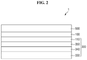
- FIG. 2 is a schematic partial cross-sectional view illustrating the display device of FIG. 1 .
- FIG. 3 is a block diagram of a touch sensor shown in FIG. 1 .
- the terms “above,” “top” and “upper surface” used herein refer to an upward direction (i.e., a Z-axis direction) with respect to a display panel 300 .
- the terms “below,” “bottom” and “lower surface” used herein refer to a downward direction (i.e., a direction opposite to the Z-axis direction) with respect to the display panel 300 .
- “left”, “right”, “upper” and “lower” indicate directions when the display panel 300 is viewed from the plane.
- left refers to a direction opposite to an X-axis direction
- right refers to the X-axis direction
- upper refers to a Y-axis direction
- lower refers to a direction opposite to the Y-axis direction.
- a display device 1 of one exemplary embodiment may include a touch sensor TSM, a display panel 300 and a panel driver 400 .
- the touch sensor TSM may include a sensor portion 100 and a controller 200 .
- FIG. 1 illustrates that the sensor portion 100 and the display panel 300 are separated from each other, this is merely for convenience of description and the present disclosure is not limited thereto.
- the sensor portion 100 and the display panel 300 may be integrally formed.
- the display panel 300 includes a display area DA and a non-display area NDA surrounding at least one area of the display area DA.
- the display panel 300 may include a circuit driving layer 340 disposed on a base substrate 330 and a light emitting element 350 disposed on the circuit driving layer 340 .
- the circuit driving layer 340 may include scan lines 310 , data lines 320 and a plurality of thin film transistors for driving the light emitting element 350 .
- the display area DA of the circuit driving layer 340 may be provided with a plurality of scan lines 310 and data lines 320 connected to the plurality of pixels P.
- the non-display area NDA of the circuit driving layer 340 may be provided with various driving signals for driving the pixels P and/or wirings for supplying driving power.
- the type of the display panel 300 is not particularly limited.
- the display panel 300 may be a self-luminous display panel such as an organic light emitting diode (OLED) display panel, a quantum dot light emitting display (QLED) panel, a micro-LED display panel, a nano-LED display panel, and the like.
- the display panel 300 may be a non-luminous display panel such as a liquid crystal display (LCD) panel, an electro-phoretic display (EPD) panel and an electro-wetting display (EWD) panel.
- the display device may further include a back-light unit for supplying light to the display panel 300 .
- a case where the display panel 300 is an organic light emitting diode display panel will be described as an example for convenience of explanation.
- the panel driver 400 is electrically connected to the display panel 300 to supply signals necessary for driving the display panel 300 .
- the panel driver 400 may include at least one of a scan driver for supplying scan signals to the scan lines 310 , a data driver for supplying data signals to the data lines 320 , and a timing controller for driving the scan driver and the data driver.
- the scan driver, the data driver and/or the timing controller may be integrated into one display IC (D-IC), but the present disclosure is not limited thereto.
- D-IC display IC
- at least one of the scan driver, the data driver and the timing controller may be integrated or mounted on the display panel 300 .
- the sensor portion 100 may be provided on at least one area of the display panel 300 .
- the sensor portion 100 may be provided on at least one surface of the display panel 300 so as to overlap the display panel 300 in a third direction (Z-axis direction) which is a thickness direction.
- the sensor portion 100 may be disposed on one surface (e.g., an upper surface), in a direction in which images are emitted, of both surfaces of the display panel 300 .
- the sensor portion 100 may be formed directly on at least one surface of both surfaces of the display panel 300 , or may be formed inside the display panel 300 .
- the sensor portion 100 may be formed directly on an outer surface (e.g., an upper surface of an upper substrate or a lower surface of a lower substrate) of the upper substrate (or a thin film encapsulation layer) or the lower substrate of the display panel 300 .
- the sensor portion 100 may be formed directly on an inner surface (e.g., a lower surface of the upper substrate or an upper surface of the lower substrate) of the upper substrate or the lower substrate.
- the sensor portion 100 includes a sensing area SA capable of sensing a touch input and a peripheral area NSA surrounding at least a part of the sensing area SA.
- the sensing area SA may be disposed to correspond to the display area DA of the display panel 300
- the peripheral area NSA may be disposed to correspond to the non-display area NDA of the display panel 300 .
- the sensing area SA of the sensor portion 100 may overlap the display area DA of the display panel 300 in the third direction (Z-axis direction)
- the peripheral area NSA of the sensor portion 100 may overlap the non-display area NDA of the display panel 300 in the third direction (Z-axis direction).
- Electrode members 120 for detecting a touch input and strain gauges 150 for detecting a touch pressure may be disposed in the sensing area SA of the sensor portion 100 .
- the electrode members 120 may be arranged in a matrix form. That is, the electrode members 120 may be arranged in a first direction (X-axis direction) and a second direction (Y-axis direction) perpendicular to the first direction (X-axis direction).
- the electrode members 120 may have a rectangular shape, but the present disclosure is not limited thereto.
- the electrode members 120 may have various shapes such as a polygonal shape and a circular shape.
- the electrode members 120 may have two or more shapes. For example, some of the electrode members 120 may have a rectangular shape, and the rest of the electrode members 120 may have a circular shape. Also, in some exemplary embodiments, the electrode members 120 may have different areas. For example, when a hole for insertion of a camera or the like is formed in the display device 1 , the electrode members 120 around the hole may have a partially removed shape along the hole shape.
- the electrode members 120 may be arranged in an island shape to be spaced apart from each other along a first direction (X-axis direction) and a second direction (Y axis direction) intersecting the first direction (X-axis direction).
- the electrode members 120 may form an electrode row in the first direction (X-axis direction) and may form an electrode column in a second direction (Y-axis direction).
- the shape, size and/or arrangement direction of the electrode members 120 are not particularly limited.
- the electrode members 120 may be configured as shown in FIG. 4 , which will be described later.
- the electrode members 120 may be electrically connected to the controller 200 and may receive a driving signal Ts for touch detection from the controller 200 . Further, the electrode members 120 may output a sensing signal Rs for touch detection to the controller 200 .
- the electrode members 120 may overlap at least one electrode of the display panel 300 .
- the electrode members 120 may overlap a cathode electrode of the display panel 300 and the like.
- the strain gauges 150 may be disposed between the electrode members 120 .
- the strain gauges 150 may be disposed on the same layer as the electrode members 120 , but may be disposed between the electrode members 120 in the second direction (Y-axis direction).
- the strain gauges 150 may be disposed between the electrode members 120 in the second direction (Y-axis direction), but the present disclosure is not limited thereto.
- the strain gauges 150 may be disposed only between some electrode members of the electrode members 120 in the second direction (Y-axis direction).
- the strain gauges 150 may be disposed between the electrode members 120 in the first direction (X-axis direction).
- the strain gauge 150 may change its resistance value by varying its length or cross-sectional area when a force is externally applied.
- the strain gauges 150 may be electrically isolated from the electrode members 120 .
- a noise sensing electrode member for sensing noise may be further provided in the sensing area SA of the sensor portion 100 .
- the controller 200 may include a touch driver 210 , a touch detector 230 and a pressure detector 250 .
- the controller 200 may be electrically connected to the sensor portion 100 to supply the driving signal Ts to the sensor portion 100 , and receive the sensing signal Rs corresponding to the driving signal Ts from the sensor portion 100 to detect the touch position. Further, the controller 200 may be electrically connected to the strain gauges 150 to detect the touch pressure.
- the touch driver 210 may provide the driving signal Ts for detecting a touch input to the electrode members 120 .
- the touch detector 230 may receive the sensing signal Rs corresponding to the driving signal Ts from the electrode members 120 and detect the presence/absence and/or position of the touch input.
- the electrode members 120 may form a first capacitance with at least one electrode provided in the display panel 300 .
- a second capacitance is generated between the finger and the electrode members 120 , and the first capacitance is changed by the second capacitance.
- the changed value of the first capacitance is transmitted to the touch detector 230 through a wiring line LL connected to the electrode member 120 touched by the finger.
- the touch detector 230 may detect the touch position by checking a sense line LL from which the value of the first capacitance is received. That is, the touch detector 230 can detect the touch position by sensing the amount of change in the self-capacitance formed in the electrode member 120 .
- the touch detector 230 may include one or more amplification circuits for amplifying the received sensing signal Rs, an analog digital converter which is connected to an output terminal of the amplification circuit, and a processor.
- the pressure detector 250 may be electrically connected to the strain gauges 150 and detect the touch pressure based on a change in the resistance value of the strain gauges 150 .
- the pressure detector 250 may include Wheatstone bridge circuit portions electrically connected to the strain gauges 150 , and the Whitestone bridge circuit portions may be provided in a number corresponding to the number of the strain gauges 150 .
- the touch driver 210 , the touch detector 230 and the pressure detector 250 may be integrated within a single touch IC, but the present disclosure is not limited thereto.
- the touch driver 210 and the touch detector 230 may be integrated within a single touch IC, and the pressure detector 250 may be located in a portion other than the inside of the touch IC.
- the pressure detector 250 may be disposed on the display panel 300 , or may be disposed on a separate flexible circuit board.
- a protective layer 500 may be disposed on the sensor portion 100 .
- the protective layer 500 may include, for example, a window member.
- the protective layer 500 may be attached onto the sensor portion 100 by an optical transparent adhesive or the like.
- the display device 1 may further include an optical member.
- an optical member such as a polarizing film may be interposed between the sensor portion 100 and the protective layer 500 .
- FIG. 4 is a plan view of a touch sensor according to an exemplary embodiment.
- FIG. 5 is a plan view of a touch sensor according to another exemplary embodiment.
- FIG. 6 is an enlarged plan view showing portion A of FIG. 4 according to an exemplary embodiment.
- FIG. 7 is an enlarged plan view showing portion A of FIG. 4 according to another exemplary embodiment.
- FIG. 8 is a plan view showing a resistance line according to another exemplary embodiment.
- FIG. 9 is a plan view showing a resistance line according to another exemplary embodiment.
- FIG. 10 is a plan view showing a resistance line according to still another exemplary embodiment.
- FIG. 11 is a cross-sectional view taken along a sectional line I-I′ of FIG. 4 .
- the touch sensor TSM includes a sensor portion 100 and a controller 200 . Since the controller 200 has been described in detail with reference to FIG. 3 , a redundant description will be omitted.
- the sensor portion 100 includes a base layer 110 and a sensing pattern 100 a disposed on the base layer 110 .
- the sensing pattern 100 a includes electrode members 120 and strain gauges 150 .
- the base layer 110 may include a sensing area SA and a peripheral area NSA.
- the base layer 110 is a layer serving as a base of the sensing pattern 100 a .
- the base layer 110 may be one of the layers constituting the display panel 300 .
- the base layer 110 may be at least one layer constituting the display panel 300 .
- the base layer 110 may be a thin film encapsulation (TFE) layer of the display panel 300 .
- the base layer 110 may be a rigid substrate or a flexible substrate depending on the exemplary embodiment.
- the base layer 110 may be a rigid substrate made of glass or tempered glass, or a flexible substrate formed of a thin film of a flexible plastic material.
- the base layer 110 includes at least one layer constituting the display panel 300 , for example, a layer including a thin film encapsulation layer, will be described as an example.
- the electrode members 120 On the sensing area SA of the base layer 110 , there may be disposed the electrode members 120 arranged in an island shape, the strain gauges 150 arranged between the electrode members 120 , wiring lines LL electrically connected to the electrode members 120 , and a first signal line SL 1 and a second signal line SL 2 connected to the strain gauges 150 .
- the electrode members 120 may be arranged in an island shape along the rows and the columns as described above.
- FIG. 4 illustrates that four electrode members 120 are arranged along the second direction (Y-axis direction), three electrode members 120 are arranged along the first direction (X-axis direction), a first electrode row RD 1 , a second electrode row RD 2 , a third electrode row RD 3 , and a fourth electrode row RD 4 are sequentially arranged along the second direction (Y-axis direction), and a first electrode column CD 1 , a second electrode column CD 2 , and a third electrode column CD 3 are sequentially arranged along the first direction (X-axis direction), this is merely for convenience of description and the present disclosure is not limited thereto.
- the number and arrangement of the electrode members 120 may be changed variously.
- the electrode members 120 may be disposed on the base layer 110 and may include a conductive material.
- the conductive material may include a metal or an alloy thereof.
- the metal may be at least one selected from the group consisting of gold (Au), silver (Ag), aluminum (Al), molybdenum (Mo), chromium (Cr), titanium (Ti), nickel (Ni), neodymium (Nd), copper (Cu), platinum (Pt) and the like.
- the electrode members 120 may be made of a transparent conductive material.
- the transparent conductive material may include silver nanowire (AgNW), indium tin oxide (ITO), indium zinc oxide (IZO), antimony zinc oxide (AZO), indium tin zinc oxide (ITZO), zinc oxide (ZnO), tin oxide (SnO 2 ), carbon nano tube, graphene and the like.
- the electrode members 120 may have a single-layer structure or a multilayer structure. When the electrode members 120 are formed to have a multilayer structure, the electrode members 120 may include multiple metal layers. For example, the electrode members 120 may have a three-layer structure of titanium/aluminum/titanium.
- the electrode members 120 may have a mesh structure for transmitting light outputted from the display area DA of the display panel 300 .
- the electrode members 120 may include a plurality of mesh holes MH, and a portion of the base layer 110 is exposed by the mesh holes MH.
- the mesh holes MH of the electrode members 120 may overlap a light emitting region of the display panel 300 in the third direction (Z-axis direction) which is the thickness direction. Further, the area of the mesh holes MH may be larger than the area of the light emitting region of the display panel 300 .
- the strain gauges 150 may be disposed on the sensing area SA of the base layer 110 and may be disposed on the same layer as the electrode members 120 .
- the strain gauges 150 and the electrode members 120 may not overlap each other in the third direction (Z-axis direction).
- the present disclosure is not limited thereto.
- the strain gauges 150 and the electrode members 120 may partially overlap each other in the third direction (Z-axis direction).
- the strain gauge 150 may include a resistance line 151 and a connection line 153 .
- the resistance line 151 may be disposed between the electrode members 120 in the second direction (Y-axis direction), and may be spaced apart from the electrode members 120 .
- the resistance line 151 may be bent to have a predetermined pattern. For example, when a pressure having a predetermined magnitude is applied to the sensor portion 100 of the touch sensor TSM, the length or cross-sectional area of the resistance line 151 is deformed, and the resistance value changes according to the deformation of the length or the cross-sectional area of the resistance line 151 . Thus, the magnitude of the touch pressure may be determined based on the changed resistance value.
- the resistance line 151 may be shaped to include two or more bent portions and portions extending in the first direction (X-axis direction) and a direction opposite to the first direction (X-axis direction).
- the present disclosure is not limited thereto, and the resistance line 151 may have various shapes.
- a resistance line 151 _ 1 may be shaped to include two or more bent portions and portions which extend in the second direction (Y-axis direction).
- a resistance line 151 _ 2 may be shaped to include two or more bent portions and portions which extend in the first direction (X-axis direction).
- a first resistance line 151 _ 3 may be formed to be wound in an angular spiral shape.
- the first resistance line 151 _ 3 may be formed to be wound in a curved spiral shape.
- the present disclosure is not limited thereto, and the shape of the resistance line 151 may be changed variously depending on the position and the number.
- the resistance line 151 may be disposed on the same layer as the electrode members 120 and the resistance line 151 may be formed of the same material as the electrode members 120 .
- the resistance line 151 may include a conductive material.
- the resistance line 151 and the electrode members 120 may be formed in the same process and the resistance line 151 may be formed in a mesh structure similarly to the electrode members 120 .
- the resistance line 151 may include a plurality of mesh holes MH, and a portion of the base layer 110 may be exposed by the mesh holes MH of the resistance line 151 .
- the mesh holes MH of the resistance line 151 may overlap the light emitting region of the display panel 300 in the third direction (Z-axis direction) which is the thickness direction.
- the area of the mesh holes MR of the resistance line 151 may be larger than the area of the light emitting region of the display panel 300 .
- the resistance line 151 is located on the display area DA of the display panel 300 , light outputted from the display area DA of the display panel 300 can be smoothly outputted to the outside after passing through the resistance line 151 .
- the resistance line 151 may be formed by removing a portion of the mesh structure.
- a plurality of branch portions separated from each other may be formed.
- the branch portions may be residues which remain by removing a partial region of the mesh structure.
- a dummy pattern DPT may be disposed in an area where the connection line 153 , the resistance line 151 and the electrode members 120 are not disposed.
- the dummy pattern DPT may be disposed on the same layer as the connection line 153 , the resistance line 151 and the electrode members 120 , and may be disposed to be spaced apart from the connection line 153 , the resistance line 151 and the electrode members 120 .
- the dummy pattern DPT can prevent or reduce the deterioration of image quality due to visibility of an area where the connection line 153 , the resistance line 151 and the electrode members 120 are not disposed in the display area DA.
- connection line 153 may electrically connect the resistance lines 151 disposed along the second direction (Y-axis direction) to each other.
- FIG. 4 illustrates that the connection line 153 electrically connects the three resistance lines 151 disposed along the second direction (Y-axis direction), this is merely exemplary, but the present disclosure is not limited thereto.
- the connection line 153 may electrically connect only two neighboring resistance lines 151 along the second direction (Y-axis direction).
- the connection line 153 may electrically connect the resistance lines 151 arranged along the first direction (X-axis direction) to each other.
- connection line 153 is disposed to electrically connect the resistance lines 151 arranged along the second direction (Y-axis direction), but the present disclosure is not limited thereto, and two or more connection lines 153 may be disposed. When a plurality of connection lines 153 are disposed, there is an advantage that connection reliability between the resistance lines 151 can be improved.
- connection lines 153 may be in direct contact with the resistance lines 151 and the connection lines 153 may be separated without contacting the electrode members 120 .
- connection line 153 may be disposed on the same layer as the resistance line 151 and the electrode members 120 , and the connection line 153 may be formed of the same material as the resistance line 151 and the electrode members 120 .
- the connection line 153 may include a conductive material.
- the connection line 153 may be formed in the same process as the resistance line 151 and the electrode members 120 .
- the connection line may have a mesh structure similarly to the resistance line 151 and the electrode members 120 .
- An insulating layer IL may be disposed on the electrode members 120 , the connection line 153 and the resistance line 151 .
- the insulating layer IL may cover the electrode members 120 , the connection line 153 , and the resistance line 151 . That is, the insulating layer IL may be in contact with the electrode members 120 , the connection line 153 , the resistance line 151 and the base layer 110 , and the mesh holes MH disposed in each of the electrode members 120 , the connection line 153 , and the resistance line 151 may be filled with an insulating material forming the insulating layer IL.
- the electrode members 120 and the strain gauges 150 disposed on the same layer may be electrically isolated from each other by the insulating layer IL.
- the insulating layer IL may include an insulating material.
- the insulating material may be an inorganic insulating material or an organic insulating material.
- the inorganic insulating material may include at least one of aluminum oxide, titanium oxide, silicon oxide, silicon oxynitride, zirconium oxide, and hafnium oxide.
- the organic insulating material may include at least one selected from the group consisting of an acrylic resin, a methacrylic resin, polyisoprene, a vinyl resin, an epoxy resin, a urethane resin, a cellulose resin, a siloxane resin, a polyimide resin, a polyamide resin and a perylene resin.
- the sensor portion 100 may include wiring lines LL and signal lines SL 1 and SL 2 .
- the sensor portion 100 may include a first signal line SL 1 and a second signal line SL 2 connected to the resistance lines 151 and the wiring lines LL connected to the electrode members 120 , respectively.
- One distal end of the wiring lines LL may be connected to each of the electrode members 120 , and the number of the wiring lines LL may be equal to the number of the electrode members 120 .
- n electrode members 120 are arranged in the first direction (X-axis direction)
- n wiring lines LL may be disposed corresponding to n electrode members 120 .
- m first electrode rows RD 1 each having n electrode members 120 arranged in the first direction (X-axis direction)
- Y-axis direction n ⁇ m wiring lines LL may be disposed.
- the other distal end of the n ⁇ m wiring lines LL may be connected to a pad portion TP.
- one wiring line LL may be connected to one electrode group.
- the number of wiring lines LL may be smaller than the number of the electrode members 120 .
- One distal end of the first signal line SL 1 may be connected to one distal end of the strain gauge 150 and one distal end of the second signal line SL 2 may be connected to the other distal end of the strain gauge 150 . More specifically, as shown in FIG. 4 , when one distal ends of the three resistance lines 151 arranged along the second direction (Y-axis direction) are electrically connected to each other by the connection line 153 of the strain gauge 150 , the first signal line SL 1 may be connected to the other distal end of the first resistance line 151 disposed in the second direction (Y axis direction), and the second signal line SL 2 may be connected to the other distal end of the third resistance line 151 . The other distal ends of the first signal line SL 1 and the second signal line SL 2 may be connected to the pad portion TP.
- the wiring lines LL and the first and second signal lines SL 1 and SL 2 may be arranged in the same layer as the electrode members 120 , the connection line 153 , and the resistance line 151 .
- the wiring lines LL and the first and second signal lines SL 1 and SL 2 may be made of the same material as the electrode members 120 , the connection line 153 , and the resistance line 151 .
- the wiring lines LL and the first and second signal lines SL 1 and SL 2 may include a conductive material.
- the wiring lines LL and the first and second signal lines SL 1 and SL 2 may be formed in the same process as the electrode members 120 , the connection line 153 , and the resistance line 151 , and may have a mesh structure.
- the pad portion TP includes a plurality of pads arranged along the first direction x, and the wiring lines LL and the first and second signal lines SL 1 and SL 2 may be connected to the respective pads. Further, as shown in FIG. 4 , the pad portion TP may include a signal line connection pattern CNL that electrically connects the adjacent strain gauges 150 to each other.
- the signal line connection pattern CNL may electrically connect the second signal line SL 2 of the strain gauge 150 disposed on the first electrode column CD 1 and the first signal line SL 1 of the strain gauge 150 disposed on the second electrode column CD 2 , and may electrically connect the second signal line SL 2 of the strain gauge 150 disposed on the second electrode column CD 2 and the first signal line SL 1 of the strain gauge 150 disposed on the third electrode column CD 3 .
- the strain gauge 150 disposed on the first electrode column CD 1 , the strain gauge 150 disposed on the second electrode column CD 2 , and the strain gauge 150 disposed on the third electrode column CD 3 may sense a pressure with one sensor.
- the present disclosure is not limited thereto. As shown in FIG.
- a pad portion TP of a sensor portion 100 _ 1 may not include a signal line connection pattern CNL for electrically connecting the adjacent strain gauges 150 to each other.
- the strain gauge 150 disposed on the first electrode column CD 1 , the strain gauge 150 disposed on the second electrode column CD 2 , and the strain gauge 150 disposed on the third electrode column CD 3 may sense a pressure with a first pressure sensor GR 1 , a second pressure sensor GR 2 , and a third pressure sensor GR 3 , respectively.
- the strain gauges 150 can be grouped through the signal line connection pattern CNL, and the arrangement of the signal line connection pattern CNL can be modified variously.
- the touch sensor TSM since all of the electrode members 120 , the strain gauge 150 , the wiring lines LL and the first and second signal lines SL 1 and SL 2 are disposed in the same layer in the sensing area SA, there is an advantage that the electrode members 120 , the strain gauge 150 , the wiring lines LL and the first and second signal lines SL 1 and SL 2 can be simultaneously formed through a single mask process. Thus, by simplifying a manufacturing process of the display device 1 , the productivity can be effectively improved, and the touch sensor TSM can be realized in a thin shape.
- the base layer 110 serving as a base of the sensor portion 100 may be a thin film encapsulation (TFE) layer of the organic light emitting diode display panel.
- the base layer 110 may be embodied as a multilayer including at least one organic film and at least one inorganic film, or may be embodied as a single layer including a combination of organic and inorganic materials.
- the base layer 110 may be a multilayer including at least two inorganic films and at least one organic film interposed between the inorganic films.
- the components of the display panel 300 may be disposed on one surface of the base layer 110 and the electrodes constituting the sensor portion 100 may be disposed on the other surface of the base layer 110 .
- FIG. 12 is a schematic view showing an arrangement relationship between pixels and a sensor portion of a display panel according to an exemplary embodiment.
- FIG. 13 is a cross-sectional view taken along a sectional line II-IP of FIG. 12 .
- FIG. 12 exemplarily shows a region where the insulating layer IL and the electrode members 120 of FIG. 4 overlap each other in a plan view.
- the strain gauge 150 , the wiring lines LL and the first and second signal lines SL 1 and SL 2 forming the mesh structure may also have the same arrangement relationship with the pixels of the display panel 300 .
- the display panel 300 includes a plurality of pixels P.
- Each pixel P may include a light emitting region EMA and a non-light emitting region NEM.
- the pixel P may include a first color pixel, a second color pixel and a third color pixel.
- Each color pixel P may be arranged in various ways.
- a first color pixel e.g., a red pixel
- a second color pixel e.g., a blue pixel
- a third color pixel e.g., a green pixel
- the pixels belonging to the second row may be arranged alternately in the first direction (X-axis direction) with respect to the pixels belonging to the first row.
- the number of the third color pixels belonging to the second row may be twice the number of the first color pixels or the second color pixels belonging to the first row.
- the arrangement of the first row and the second row may be repeated along the first direction (X-axis direction).
- the size of the light emitting region EMA in each color pixel P may be different.
- a light emitting region EMA_B of the second color pixel may be larger than a light emitting region EMA_R of the first color pixel
- a light emitting region EMA_G of the third color pixel may be smaller than a light emitting region EMA_R of the first color pixel.
- the shape of the light emitting region EMA of each color pixel P may be substantially octagonal.
- the present disclosure is not limited thereto, and the shape of each light emitting region EMA may be a circular shape, other polygonal shapes such as a rhombus shape, a rounded polygonal shape, or the like.
- the electrode members 120 may be divided into mesh holes MH and a body part BP.
- the mesh holes MH may overlap the light emitting region EMA in the thickness direction, and the area of the mesh holes MH may be larger than the area of the light emitting region EMA.
- the body part BP may overlap the non-light emitting region NEM in the thickness direction, and the width of the body part BP may be smaller than the width of the non-light emitting region NEM.
- a first electrode EL 1 is disposed for each pixel on the base substrate 330 .
- a pixel defining layer PDL that exposes the first electrode EL 1 may be disposed on the first electrode EL 1 .
- the pixel defining layer PDL is disposed in the non-light emitting region NEM.
- a light emitting layer EML may be disposed on the first electrode EL 1 exposed by the pixel defining layer PDL, and a second electrode EL 2 may be disposed thereon.
- the second electrode EL 2 may be disposed over the entire surface irrespective of pixels.
- the first electrode EL 1 , the light emitting layer EML and the second electrode EL 2 constitute the light emitting element 350 , respectively.
- a thin film encapsulation layer 1100 including a first inorganic film 1101 , an organic film 1102 , and a second inorganic film 1103 may be disposed on the second electrode EL 2 , and the electrode members 120 and the insulating layer IL may be arranged sequentially thereon.
- the body part BP may be disposed to overlap the pixel defining layer PDL, and may be located in the non-light emitting region NEM. That is, since the body part BP does not overlap the light emitting region EMA, it may not interfere with the light emission.
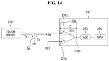
- FIG. 14 is a diagram explaining a touch position detecting operation of a touch sensor according to an exemplary embodiment.
- the touch driver 210 may provide the driving signal Ts to the electrode members 120 with a capacitance Cs through the wiring lines LL, and the touch detector 230 may receive the sensing signal Rs from electrode members 130 through the wiring lines LL.
- the sensing signal Rs may include information on the amount of change in self-capacitance formed in the electrode members 120 , as described above.
- the touch detector 230 may include at least one first amplification circuit 231 such as an operational amplifier, an analog-to-digital converter (ADC) 233 , and a processor (MPU) 235 .
- ADC analog-to-digital converter
- MPU processor
- the first amplification circuit 231 may include a first input terminal 231 a , a second input terminal 231 b and an output terminal 231 c .
- the first input terminal 231 a of the first amplification circuit 231 e.g., an inverting input terminal of the operational amplifier, may be electrically connected to the electrode members 130 via the wiring line LL or the like.
- the sensing signal Rs may be inputted to the first input terminal 231 a.
- the second input terminal 231 b of the first amplification circuit 231 is a reference potential terminal, and may be connected to a reference power source REF as an example.
- the reference power source may be a ground (GND) power source.
- the present disclosure is not limited thereto.
- the second input terminal 231 b may be electrically connected to the noise sensing electrode member.
- the touch sensor TSM can effectively cancel a noise signal inputted from the display panel 300 and the like, and improve a signal-to-noise ratio (SNR). Accordingly, it is possible to minimize the malfunction of the touch sensor TSM according to the noise signal and improve the sensing sensitivity.
- SNR signal-to-noise ratio
- a capacitor C and a reset switch SW may be connected in parallel between the first input terminal 231 a and the output terminal 231 c of the first amplification circuit 231 .
- the first amplification circuit 231 is implemented as an inverting amplification circuit, the present disclosure is not limited thereto. In other exemplary embodiments, the first amplification circuit 231 may be implemented in the form of a non-inverting amplification circuit or the like.
- the output terminal 231 c of the first amplification circuit 231 may be electrically connected to the analog-to-digital converter 233 .
- the analog-to-digital converter 233 may convert an input analog signal into a digital signal. According to the exemplary embodiment, the analog-to-digital converter 233 may be provided as many as the number of the electrode members 120 in one-to-one correspondence. Alternatively, in another exemplary embodiment, the electrode members 120 may be configured to share one analog-to-digital converter 233 , and in this case, a switching circuit for channel selection may be additionally provided.
- the processor 235 processes the converted signal (digital signal) from the analog-to-digital converter 233 , and detects the touch input according to the signal processing result.
- the processor 235 may comprehensively analyze the sensing signal amplified by the first amplification circuit 231 and converted by the analog-to-digital converter 233 to detect whether or not a touch input has occurred and its position.
- the processor 235 may be implemented as a microprocessor (MPU).
- a memory required for driving the processor 235 may be additionally provided in the touch detector 230 .
- the configuration of the processor 235 is not limited thereto.
- the processor 235 may be implemented as a microcontroller (MCU) or the like.
- FIG. 15 is a diagram schematically showing an arrangement of signal lines and a strain gauge of a touch sensor and a connection relationship with a Wheatstone bridge circuit portion according to an exemplary embodiment.
- FIG. 16 is a diagram schematically showing a first pressure detector including a first Wheatstone bridge circuit portion electrically connected to a first strain gauge of a touch sensor according to an exemplary embodiment.
- the first strain gauge 150 may include one distal end E 1 a and the other distal end E 2 a separated from each other by a predetermined distance along the second direction (Y-axis direction). As described above, one distal end E 1 a of the first strain gauge 150 may be connected to the first signal line SL 1 and the other distal end E 2 a of the first strain gauge 150 may be connected to the second signal line SL 2 .
- strain gauge 150 may be disposed on the sensing area SA as described above. That is, the Wheatstone bridge circuit portion WB electrically connected to the strain gauge 150 may also be provided on the controller 200 in a number corresponding to the number of the strain gauges 150 arranged for individual connection.
- the pressure detector 250 may include the Wheatstone bridge circuit portion WB.
- the pressure detector 250 may further include an analog-to-digital converter and a processor for detecting a first voltage Va outputted from the Wheatstone bridge circuit portion WB.
- the Wheatstone bridge circuit portion WB includes a first node N 1 , a second node N 2 , a first output node N 3 , and a second output node N 4 .
- a driving voltage Vs may be provided to the first node N 1 , and the second node N 2 may be connected to the ground GND.
- the Wheatstone bridge circuit portion WB may further include a first resistor WBa connected to the second node N 2 and the second output node N 4 , a second resistor WBb connected to the first node N 1 and the second output node N 4 , and a third resistor WBc connected to the second node N 2 and the first output node N 3 .
- a resistance value R 1 of the first resistor WBa, a resistance value R 2 of the second resistor WBb, and a resistance value R 3 of the third resistor WBc may have predetermined values, respectively. That is, the first to third resistors WBa, WBb, and WBc may be fixed resistors.
- the Wheatstone bridge circuit portion WB may further include a second amplification circuit 251 a such as an operational amplifier.
- the second amplification circuit 251 a may include an inverting input terminal, a non-inverting input terminal and an output terminal. Through the second amplification circuit 251 a , it is possible to sense an electrical flow between the first output node N 3 and the second output node N 4 .
- the second amplification circuit 251 a may operate as a galvanometer element or a voltage measuring element.
- One of the first output node N 3 and the second output node N 4 may be electrically connected to one of the input terminals of the second amplification circuit 251 a and the other one may be electrically connected to another input terminal of the second amplification circuit 251 a .
- the first output node N 3 may be connected to the inverting input terminal of the second amplification circuit 251 a
- the second output node N 4 may be connected to the non-inverting input terminal of the second amplification circuit 251 a.
- the output terminal of the second amplification circuit 251 a may output a first voltage Va proportional to a difference between the voltage values inputted to the both input terminals.
- One distal end E 1 a of the strain gauge 150 may be electrically connected to the first node N 1 via the first signal line SL 1 , and the other distal end E 2 a of the strain gauge 150 may be connected to the first output node N 3 via the second signal line SL 2 .
- the strain gauge 150 , the first resistor WBa, the second resistor WBb and the third resistor WBc may be connected to each other to implement the Wheatstone bridge circuit portion WB.
- the product of the resistance value Ra of the strain gauge 150 and the resistance value R 1 of the first resistor WBa may be substantially equal to the product of the resistance value R 2 of the second resistor WBb and the resistance value R 3 of the third resistor WBc.
- the voltage of the first output node N 3 and the voltage of the second output node N 4 may be equal to each other.
- the voltage difference between the first output node N 3 and the second output node N 4 is 0 V, and the first voltage Va outputted by the second amplification circuit 251 a may be 0 V.
- the shape of the strain gauge 150 may be deformed according to the intensity of the touch, and the resistance value Ra of the strain gauge 150 may be changed by the shape deformation. Accordingly, a voltage difference is generated between the first output node N 3 and the second output node N 4 .
- the second amplification circuit 251 a outputs a value other than 0 V as the first voltage Va, and the touch sensor can measure the intensity of the touch or the pressure of the touch by measuring it.
- FIG. 17 is a plan view of a touch sensor according to another exemplary embodiment
- FIG. 18 is a plan view of a touch sensor according to another exemplary embodiment
- FIG. 19 is a block diagram of the touch sensor shown in FIG. 17
- FIG. 20 is an enlarged plan view of portion B of FIG. 17 according to an exemplary embodiment
- FIG. 21 is an enlarged plan view of portion B of FIG. 17 according to another exemplary embodiment
- FIG. 22 is a cross-sectional view taken along a sectional line of FIG. 17 .
- the exemplary embodiment of FIGS. 17, 18, 19, 20, 21, and 22 is different from the exemplary embodiment of FIGS. 4, 5, 6, 7, 8, 9, 10, and 11 in the structure of the electrode member and the shape of the strain gauge. A description overlapping with the exemplary embodiment with reference to FIGS. 4, 5, 6, 7, 8, 9, 10, and 11 will be omitted, and differences will be mainly described.
- electrode members 120 _ 1 for detecting a touch input may be disposed in the sensing area SA of a sensor portion 100 _ 2 , and the electrode members 120 _ 1 may be arranged to be spaced apart from each other in the first direction (X-axis direction).
- the electrode members 120 _ 1 may be disposed in the first electrode column CD 1 , the second electrode column CD 2 , and the third electrode column CD 3 , respectively.
- the following description will be given with respect to the electrode members 120 _ 1 disposed in the first electrode column CD 1 .
- a first electrode member 121 may have a bar shape extending in the second direction (Y-axis direction).
- the plurality of first electrode members 121 may be arranged to be spaced apart from each other in the second direction (Y-axis direction).
- the first electrode members 121 may be disposed in the first electrode row RD 1 , the second electrode row RD 2 , and the third electrode row RD 3 , respectively.
- a second electrode member 123 may include a first unit 123 a and a second unit 123 b extending along the second direction (Y-axis direction), and the second electrode members 123 may be arranged to be spaced apart from each other in the first direction (X-axis direction).
- the first electrode members 121 and the second electrode members 123 may be spaced apart from each other and electrically isolated from each other.
- Each of the first unit 123 a and the second unit 123 b may include a connection portion CP connecting the protrusion portions PP and the protrusion portions PP in the second direction (Y-axis direction).
- the protrusion portions PP of the first unit 123 a and the protrusion portions PP of the second unit 123 b may be spaced apart from each other by a predetermined distance in the second direction (Y-axis direction) and may be alternately arranged.
- connection portion CP of the first unit 123 a may connect the protrusion portions PP of the first unit 123 a at one distal end of the protrusion portions PP of the first unit 123 a
- connection portion CP of the second unit 123 b may connect the protrusion portions PP of the second unit 123 b at the other distal end of the protrusion portions PP of the second unit 123 b
- the protrusion portion PP of the first unit 123 a and the protrusion portion PP of the second unit 123 b may be located between the connection portion CP of the first unit 123 a and the connection portion CP of the second unit 123 b.
- Each of the first electrode members 121 and the second electrode members 123 may be electrically connected to the controller 200 .
- the second electrode member 123 may be a driving electrode member that receives the driving signal Ts for touch detection from the controller 200
- the first electrode member 121 may be a sensing electrode member that outputs the sensing signal Rs for touch detection to the controller 200 .
- each of the first electrode members 121 and the second electrode members 123 may have a mesh structure for transmitting light outputted from the display area DA of the display panel 300 .
- each of the first electrode members 121 and the second electrode members 123 may include a plurality of mesh holes MH.
- the sensing area SA of the sensor portion 100 may be provided with the strain gauge 150 for detecting the touch pressure.
- the strain gauge 150 may be disposed between the electrode members 120 _ 1 .
- the strain gauge 150 may be disposed on the same layer as the electrode members 120 _ 1 , and the strain gauge 150 may not overlap the electrode members 120 _ 1 in the thickness direction.
- the strain gauge 150 may include a resistance line 151 disposed between the protrusion portion PP of the first unit 123 a and the protrusion portion PP of the second unit 123 b , and a connection line 153 connecting the adjacent resistance lines 151 .
- the resistance line 151 may be shaped to include two or more bent portions and portions extending in the first direction (X-axis direction) and a direction opposite to the first direction (X-axis direction).
- the present disclosure is not limited thereto, and the resistance line 151 may have various shapes as described above.
- the strain gauge 150 may have a mesh structure similarly to the first electrode members 121 and the second electrode members 123 .
- the strain gauge 150 may include a plurality of mesh holes MH.
- the strain gauge 150 may change its resistance value by varying its length or cross-sectional area when a force is externally applied.
- the insulating layer IL may be disposed on the first electrode members 121 and the second electrode members 123 , the connection line 153 , and the resistance line 151 .
- the insulating layer IL may cover the electrode members 120 , the connection line 153 , and the resistance line 151 .
- the strain gauge 150 may be electrically isolated from the first electrode members 121 and the second electrode members 123 .
- the sensing area SA may include a touch position sensing area TSA where the first electrode members 121 and the second electrode members 123 are disposed and a touch pressure sensing area PSA where the resistance line 151 is disposed.
- the touch driver 210 may provide the driving signal Ts for detecting a touch input to the second electrode members 123 .
- the touch detector 230 may receive the sensing signal Rs corresponding to the driving signal Ts from the first electrode members 121 and detect the presence/absence and/or position of the touch input.
- the sensing signal Rs may be an amount of mutual capacitance change occurring between the first electrode members 121 and the second electrode members 123 .
- the touch detector 230 may receive a change amount of mutual capacitance between the first electrode members 121 and the second electrode members 123 as a sensing signal Rs to determine the presence/absence and/or position of the touch input. Further, the touch pressure can be detected based on the resistance value change of the strain gauge 150 through the pressure detector 250 .
- the sensor portion 100 _ 2 may include first wiring line LL 1 and second wiring line LL 2 and a first signal line SL 1 and a second signal line SL 2 .
- the sensor portion 100 _ 2 may include a first wiring line LL 1 connected to each of the first electrode members 121 , a second wiring line LL 2 connected to each of the second electrode members 123 , and a first signal line SL 1 and a second signal line SL 2 connected to the resistance line 151 .
- first wiring line LL 1 may be connected to the first electrode members 121 and one distal ends of the second wiring line LL 2 may be connected to the second electrode members 123 , respectively.
- the second wiring line LL 2 may include a second-first wiring line LL 2 _ 1 and a second-second wiring line LL 2 _ 2 .
- One distal end of the second-first wiring line LL 2 _ 1 may be connected to the first unit 123 a and one distal end of the second-second wiring line LL 2 _ 2 may be connected to the second unit 123 b .
- the other distal ends of the first wiring line LL 1 and the second wiring line LL 2 may be connected to the pad portion TP.
- first signal line SL 1 may be connected to one distal end of the strain gauge 150 and one distal end of the second signal line SL 2 may be connected to the other distal end of the strain gauge 150 . More specifically, the first signal line SL 1 may be connected to one distal end (opposite to the other distal end to which the connection line is connected) of the resistance line 151 disposed on the uppermost side arranged along the second direction (Y-axis direction). The second signal line SL 2 may be connected to the other distal end (opposite to one distal end to which the connection line is connected) of the resistance line 151 disposed first along the second direction (Y-axis direction). Further, the other distal ends of the first signal line SL 1 and the second signal line SL 2 may be connected to the pad portion TP.
- the first and second wiring lines LL 1 and LL 2 and the first and second signal lines SL 1 and SL 2 may be disposed on the same layer as the electrode members 120 _ 1 , the connection line 153 , and the resistance line 151 .
- the first and second wiring lines LL 1 and LL 2 and the first and second signal lines SL 1 and SL 2 may be formed of the same material and by the same process as the electrode members 120 _ 1 , the connection line 153 , and the resistance line 151 and may have a mesh structure.
- the pad portion TP includes a plurality of pads arranged along the first direction (X-axis direction), and the first and second wiring lines LL 1 and LL 2 and the first and second signal lines SL 1 and SL 2 may be connected to the respective pads. Further, as shown in FIG. 17 , the pad portion TP may include a signal line connection pattern CNL that electrically connects the adjacent strain gauges 150 to each other. Since the arrangement structure of the signal line connection pattern CNL is the same as in FIGS. 4 and 5 , a redundant description will be omitted.
- FIG. 23 is a cross-sectional view of a touch sensor according to another exemplary embodiment.
- FIG. 24 is a plan view of a temperature compensation module of a touch sensor according to another exemplary embodiment.
- the exemplary embodiment of FIGS. 23 and 24 is different from the exemplary embodiment of FIGS. 1, 2, 3, 4, 5, 6, 7, 8, 9, 10, 11, 12, 13, 14, 15, 16, 17, 18, 19, 20, 21 , and 22 in that the touch sensor TSM further includes a temperature compensation module TRM.
- TRM temperature compensation module
- the temperature compensation module TRM may include a temperature compensation portion 101 and a controller 200 _ 1 .
- the temperature compensation portion 101 may be disposed so as to overlap the sensor portion 100 (see FIG. 1 ).
- the area where the temperature compensating portion 101 senses and compensates the temperature may correspond to the sensing area SA where the sensor portion 100 can sense the touch input.
- the temperature compensating portion 101 may be disposed between the display panel 300 (see FIG. 1 ) and the sensor portion 100 (see FIG. 1 ).
- the sensing area SA may include a touch position sensing area TSA in which the electrode members 120 are disposed, a touch pressure sensing area PSA in which the resistance line 151 is disposed, and a temperature compensation area TRA in which a temperature compensating resistance line 171 is disposed.
- the temperature compensation portion 101 includes a temperature compensating pattern 170 and temperature compensating signal lines TSL 1 and TSL 2 connected thereto.
- the temperature compensating pattern 170 and the temperature compensating signal lines TSL 1 and TSL 2 connected thereto may be disposed on the base layer 110 , and may have a mesh structure.
- the temperature compensating pattern 170 may be disposed corresponding to the strain gauge 150 of FIG. 4 .
- the temperature compensating pattern 170 and the strain gauge 150 may overlap each other in the thickness direction.
- the temperature compensating pattern 170 may include a temperature compensating resistance line 171 and a temperature compensating connection line 173 .
- the temperature compensating resistance line 171 may have the same shape as the resistance line 151 of the strain gauge 150 .
- the temperature compensating resistance line 171 may be bent to have a predetermined pattern corresponding to the resistance line 151 .
- the present disclosure is not limited thereto, and the shape of the temperature compensating resistance line 171 may be different from that of the resistance line 151 .
- the resistance value of the temperature compensating resistance line 171 may be the same as the resistance value of the resistance line 151 .
- the temperature compensating connection line 173 may electrically connect the temperature compensating resistance lines 171 disposed along the second direction (Y-axis direction) to each other.
- a first insulating layer IL 1 may be disposed on the first temperature compensating pattern 170 , and the first insulating layer IL 1 may provide a space in which the sensing pattern 100 a (see FIG. 4 ) of the sensor portion 100 (see FIG. 1 ) is disposed. It is needless to say that the sensing pattern 100 a may employ the sensing pattern 100 a described with reference to FIGS. 1, 2, 3, 4, 5, 6, and 7 or the sensing pattern 100 a described with reference to FIGS. 18, 19, 20, 21, and 22 .
- the first insulating layer IL 1 may be embodied as a multilayer including at least one organic film and at least one inorganic film, or may be embodied as a single layer including a combination of organic and inorganic materials.
- the temperature compensating signal lines TSL 1 and TSL 2 may include a first temperature compensating signal line TSL 1 connected to one distal end of the temperature compensating pattern 170 and a second temperature compensating signal line TSL 2 connected to the other distal end of the temperature compensating pattern 170 .
- the temperature compensating signal lines TSL 1 and TSL 2 may be connected to the pad portion TP to transmit signals to the controller 200 _ 1 .
- the resistance value of the strain gauge 150 may be changed according to the intensity of the touch input.
- the resistance value of the strain gauge 150 may be changed according to the body temperature of the user or the temperature change of the lower display panel 300 . Therefore, since a portion of the change amount of the resistance value of the first strain gauge 150 based on the temperature change is independent of the intensity of the user's touch input, it may act as noise.
- the temperature compensating pattern 170 is overlappingly disposed below the corresponding strain gauge 150 .
- the resistance value of the strain gauge 150 changes according to the user's body temperature or the temperature change of the lower display panel 300 .
- the temperature compensating pattern 170 also changes its resistance value by the user's body temperature or heat transmitted from the lower display panel 300 . Therefore, it is possible to compensate the component based on the temperature change in the change amount of the resistance value of the strain gauge 150 by using the resistance value change generated based on the temperature change in the temperature compensating pattern 170 .
- FIG. 25 is a diagram schematically showing an arrangement of signal lines, a temperature compensating pattern and a strain gauge of a touch sensor and a connection relationship with a Wheatstone bridge circuit portion according to another exemplary embodiment.
- FIG. 26 is a diagram schematically showing a Wheatstone bridge circuit portion electrically connected to a temperature compensating pattern and a strain gauge of a touch sensor according to still another exemplary embodiment.
- the exemplary embodiment of FIGS. 25 and 26 is different from the exemplary embodiment of FIGS. 15 and 16 in that a Wheatstone bridge circuit portion WB_ 1 of a pressure detector 250 _ 1 includes a temperature compensating pattern 170 .
- a description overlapping with the exemplary embodiment with reference to FIGS. 15 and 16 will be omitted, and differences will be mainly described.
- One distal end E 1 a of the strain gauge 150 may be electrically connected to the first node N 1 via the first signal line SL 1 , and the other distal end E 2 a of the strain gauge 150 may be connected to the first output node N 3 via the second signal line SL 2 .
- One distal end E 1 ta of the first temperature compensating pattern 170 may be connected to the second node N 2 via the first temperature compensating signal line TSL 1 , and the other distal end E 2 ta of the first temperature compensating pattern 170 may be connected to the first output node N 3 via the second temperature compensating signal line TSL 2 .
- the strain gauge 150 , the temperature compensating pattern 170 , the first resistor WBa, and the second resistor WBb may be connected to each other to form a Wheatstone bridge.
- the product of the resistance value Ra of the strain gauge 150 and the resistance value R 1 of the first resistor WBa may be substantially equal to the product of the resistance value Rta of the temperature compensating pattern 170 and the resistance value R 2 of the second resistor WBb.
- the resistance value Ra of the strain gauge 150 includes a component (hereinafter, referred to as a “first pressure resistance component”) which changes with shape deformation according to the touch pressure and a component (hereinafter, referred to as a “first temperature resistance component”) which changes based on a temperature change.
- the resistance value Rta of the temperature compensating pattern 170 includes a component (hereinafter, referred to as a “second pressure resistance component”) which changes with shape deformation according to the touch pressure and a component (hereinafter, referred to as a “second temperature resistance component” which changes based on a temperature change.
- the second pressure resistance component may be negligibly small or may exhibit a significant difference from the first pressure resistance component.
- the second temperature resistance component of the temperature compensating pattern 170 may compensate or offset the first temperature resistance component of the strain gauge 150 , thereby more sensitively detecting the touch pressure.
Abstract
Description
Claims (21)
Applications Claiming Priority (2)
| Application Number | Priority Date | Filing Date | Title |
|---|---|---|---|
| KR10-2019-0027846 | 2019-03-12 | ||
| KR1020190027846A KR20200109401A (en) | 2019-03-12 | 2019-03-12 | Touch sensor and display device |
Publications (2)
| Publication Number | Publication Date |
|---|---|
| US20200293149A1 US20200293149A1 (en) | 2020-09-17 |
| US11216136B2 true US11216136B2 (en) | 2022-01-04 |
Family
ID=72423242
Family Applications (1)
| Application Number | Title | Priority Date | Filing Date |
|---|---|---|---|
| US16/673,373 Active US11216136B2 (en) | 2019-03-12 | 2019-11-04 | Touch sensor and display device |
Country Status (3)
| Country | Link |
|---|---|
| US (1) | US11216136B2 (en) |
| KR (1) | KR20200109401A (en) |
| CN (1) | CN111694457A (en) |
Families Citing this family (3)
| Publication number | Priority date | Publication date | Assignee | Title |
|---|---|---|---|---|
| FR3053116B1 (en) * | 2017-01-14 | 2018-08-24 | Nanomade Concept | SENSOR AND TOUCH SCREEN WITH ENVIRONMENTAL COMPENSATION, PARTICULARLY IN TEMPERATURE |
| KR20200120821A (en) * | 2019-04-12 | 2020-10-22 | 삼성디스플레이 주식회사 | Touch sensor and display device |
| JP2020194215A (en) * | 2019-05-24 | 2020-12-03 | 日本航空電子工業株式会社 | Touch panel |
Citations (13)
| Publication number | Priority date | Publication date | Assignee | Title |
|---|---|---|---|---|
| US7663607B2 (en) | 2004-05-06 | 2010-02-16 | Apple Inc. | Multipoint touchscreen |
| KR101373044B1 (en) | 2012-04-19 | 2014-03-11 | 삼성디스플레이 주식회사 | Touch Screen Panel |
| US9690413B2 (en) | 2014-01-13 | 2017-06-27 | Apple Inc. | Temperature compensating transparent force sensor having a compliant layer |
| US20170285864A1 (en) * | 2016-03-31 | 2017-10-05 | Apple Inc. | Electronic Device Having Direction-Dependent Strain Elements |
| US20170285799A1 (en) * | 2016-03-29 | 2017-10-05 | Japan Display Inc. | Detecting apparatus and display apparatus |
| KR101811417B1 (en) | 2017-04-10 | 2017-12-21 | 주식회사 하이딥 | Touch pressure detectable touch input device including display module |
| US20180074638A1 (en) * | 2016-09-14 | 2018-03-15 | Tpk Touch Solutions (Xiamen) Inc. | Pressure sensing module and pressure sensing touch control system using the same |
| US20180085061A1 (en) * | 2016-09-28 | 2018-03-29 | International Business Machines Corporation | Characterizing primate nail deformation |
| US10095351B2 (en) | 2016-03-31 | 2018-10-09 | Boe Technology Group Co., Ltd. | Substrate, display device and force identification method |
| US20180299335A1 (en) * | 2015-08-17 | 2018-10-18 | Institute Of Ceology And Geophysics, Chinese Academy Of Sciences | Mems strain gauge sensor and manufacturing method |
| US20190004659A1 (en) * | 2017-06-30 | 2019-01-03 | Shanghai Tianma Micro-electronics Co., Ltd. | Display panel and display device |
| US20190178730A1 (en) * | 2017-12-07 | 2019-06-13 | Texas Instruments Incorporated | Magnetostrictive strain gauge sensor |
| US20200167029A1 (en) * | 2018-08-24 | 2020-05-28 | Tpk Advanced Solutions Inc. | Pressure sensing module, touch panel and method of detecting two-point touch pressure of touch panel |
Family Cites Families (3)
| Publication number | Priority date | Publication date | Assignee | Title |
|---|---|---|---|---|
| KR20180090936A (en) * | 2017-02-03 | 2018-08-14 | 삼성디스플레이 주식회사 | Touch sensor and display device having the touch sensor |
| KR102421678B1 (en) * | 2017-07-20 | 2022-07-19 | 삼성디스플레이 주식회사 | Touch sensor and display device having the same |
| KR20200052483A (en) * | 2018-11-06 | 2020-05-15 | 삼성디스플레이 주식회사 | Touch sensor and display device |
-
2019
- 2019-03-12 KR KR1020190027846A patent/KR20200109401A/en not_active Application Discontinuation
- 2019-11-04 US US16/673,373 patent/US11216136B2/en active Active
-
2020
- 2020-02-07 CN CN202010082789.5A patent/CN111694457A/en active Pending
Patent Citations (16)
| Publication number | Priority date | Publication date | Assignee | Title |
|---|---|---|---|---|
| KR101233479B1 (en) | 2004-05-06 | 2013-02-14 | 애플 인크. | Multipoint touchscreen |
| US7663607B2 (en) | 2004-05-06 | 2010-02-16 | Apple Inc. | Multipoint touchscreen |
| KR101373044B1 (en) | 2012-04-19 | 2014-03-11 | 삼성디스플레이 주식회사 | Touch Screen Panel |
| US9239654B2 (en) | 2012-04-19 | 2016-01-19 | Samsung Display Co., Ltd. | Touch screen panel |
| US9690413B2 (en) | 2014-01-13 | 2017-06-27 | Apple Inc. | Temperature compensating transparent force sensor having a compliant layer |
| US20180299335A1 (en) * | 2015-08-17 | 2018-10-18 | Institute Of Ceology And Geophysics, Chinese Academy Of Sciences | Mems strain gauge sensor and manufacturing method |
| US20170285799A1 (en) * | 2016-03-29 | 2017-10-05 | Japan Display Inc. | Detecting apparatus and display apparatus |
| US10095351B2 (en) | 2016-03-31 | 2018-10-09 | Boe Technology Group Co., Ltd. | Substrate, display device and force identification method |
| US20170285864A1 (en) * | 2016-03-31 | 2017-10-05 | Apple Inc. | Electronic Device Having Direction-Dependent Strain Elements |
| US10209830B2 (en) | 2016-03-31 | 2019-02-19 | Apple Inc. | Electronic device having direction-dependent strain elements |
| US20180074638A1 (en) * | 2016-09-14 | 2018-03-15 | Tpk Touch Solutions (Xiamen) Inc. | Pressure sensing module and pressure sensing touch control system using the same |
| US20180085061A1 (en) * | 2016-09-28 | 2018-03-29 | International Business Machines Corporation | Characterizing primate nail deformation |
| KR101811417B1 (en) | 2017-04-10 | 2017-12-21 | 주식회사 하이딥 | Touch pressure detectable touch input device including display module |
| US20190004659A1 (en) * | 2017-06-30 | 2019-01-03 | Shanghai Tianma Micro-electronics Co., Ltd. | Display panel and display device |
| US20190178730A1 (en) * | 2017-12-07 | 2019-06-13 | Texas Instruments Incorporated | Magnetostrictive strain gauge sensor |
| US20200167029A1 (en) * | 2018-08-24 | 2020-05-28 | Tpk Advanced Solutions Inc. | Pressure sensing module, touch panel and method of detecting two-point touch pressure of touch panel |
Also Published As
| Publication number | Publication date |
|---|---|
| KR20200109401A (en) | 2020-09-23 |
| US20200293149A1 (en) | 2020-09-17 |
| CN111694457A (en) | 2020-09-22 |
Similar Documents
| Publication | Publication Date | Title |
|---|---|---|
| CN113064523B (en) | Touch sensor | |
| US11875001B2 (en) | Touch sensor and display device | |
| US11314363B2 (en) | Touch sensor and display device | |
| US11681405B2 (en) | Touch sensor and display device | |
| US11301074B2 (en) | Input sensing device and display device including the same | |
| US11703969B2 (en) | Touch sensor having strain gauge and display device including the same | |
| US11216136B2 (en) | Touch sensor and display device | |
| US11231825B2 (en) | Touch sensor and display device | |
| US11681389B2 (en) | Touch sensor and display device | |
| US10824269B2 (en) | Touch sensor and display device | |
| US11662862B2 (en) | Input sensing device and display device including the same | |
| US10572051B2 (en) | Touch sensor and display device including the same | |
| US11216141B2 (en) | Touch sensor and display device | |
| KR102657639B1 (en) | Touch sensor and display device |
Legal Events
| Date | Code | Title | Description |
|---|---|---|---|
| AS | Assignment |
Owner name: SAMSUNG DISPLAY CO., LTD., KOREA, REPUBLIC OF Free format text: ASSIGNMENT OF ASSIGNORS INTEREST;ASSIGNOR:HWANG, SEONG MO;REEL/FRAME:050908/0891 Effective date: 20190925 |
|
| FEPP | Fee payment procedure |
Free format text: ENTITY STATUS SET TO UNDISCOUNTED (ORIGINAL EVENT CODE: BIG.); ENTITY STATUS OF PATENT OWNER: LARGE ENTITY |
|
| STPP | Information on status: patent application and granting procedure in general |
Free format text: NON FINAL ACTION MAILED |
|
| STPP | Information on status: patent application and granting procedure in general |
Free format text: RESPONSE TO NON-FINAL OFFICE ACTION ENTERED AND FORWARDED TO EXAMINER |
|
| STPP | Information on status: patent application and granting procedure in general |
Free format text: FINAL REJECTION MAILED |
|
| STPP | Information on status: patent application and granting procedure in general |
Free format text: ADVISORY ACTION MAILED |
|
| STPP | Information on status: patent application and granting procedure in general |
Free format text: NOTICE OF ALLOWANCE MAILED -- APPLICATION RECEIVED IN OFFICE OF PUBLICATIONS |
|
| STPP | Information on status: patent application and granting procedure in general |
Free format text: PUBLICATIONS -- ISSUE FEE PAYMENT VERIFIED |
|
| STCF | Information on status: patent grant |
Free format text: PATENTED CASE |